


Verilog n ビット双方向シフト レジスタ
デジタル エレクトロニクスでは、シフト レジスタ 出力ピンが q であるフリップフロップのカスケードです。 1 つのフロップのデータ入力ピン (d) に接続されます。すべてのフロップは同じクロックで動作するため、シフト レジスタに格納されたビット配列は 1 桁シフトします。たとえば、5 ビットの右シフト レジスタの初期値が 10110 で、シフト レジスタへの入力が 0 に接続されている場合、次のパターンは 01011 になり、次のパターンは 00101 になります。
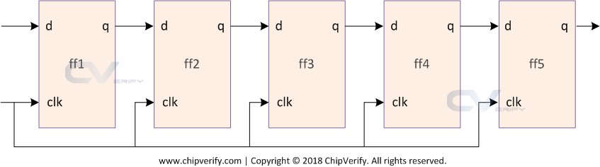
デザイン
このシフト レジスタ デザインには 5 つの入力と 1 つの n ビット出力があり、デザインは parameter を使用してパラメーター化されます。 シフト レジスタの幅を示す MSB。 n が 4 の場合、4 ビットのシフト レジスタになります。 n が 8 の場合、8 ビットのシフト レジスタになります。
このシフト レジスタには、いくつかの重要な機能があります。
- デザインのピンを駆動することで有効または無効にできます
- dir が駆動されているとき、右だけでなく左にもシフトできます
- rstn がローに引き下げられると、シフト レジスタがリセットされ、出力が 0 になります
- シフトレジスタの入力データ値はdピンで制御可能
module shift_reg  #(parameter MSB=8) (  input d,                      // Declare input for data to the first flop in the shift register
                                        input clk,                    // Declare input for clock to all flops in the shift register
                                        input en,                     // Declare input for enable to switch the shift register on/off
                                        input dir,                    // Declare input to shift in either left or right direction
                                        input rstn,                   // Declare input to reset the register to a default value
                                        output reg [MSB-1:0] out);    // Declare output to read out the current value of all flops in this register


   // This always block will "always" be triggered on the rising edge of clock
   // Once it enters the block, it will first check to see if reset is 0 and if yes then reset register
   // If no, then check to see if the shift register is enabled
   // If no => maintain previous output. If yes, then shift based on the requested direction
   always @ (posedge clk)
      if (!rstn)
         out <= 0;
      else begin
         if (en)
            case (dir)
               0 :  out <= {out[MSB-2:0], d};
               1 :  out <= {d, out[MSB-1:1]};
            endcase
         else
            out <= out;
      end
endmodule
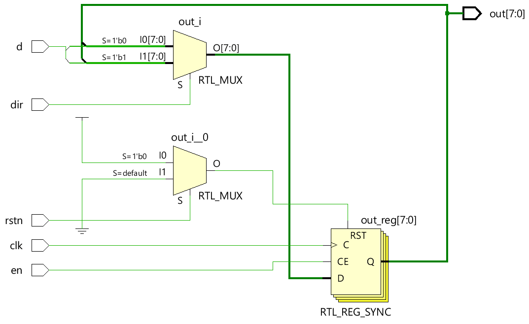
ハードウェア回路図
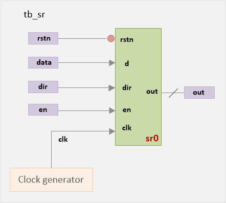
テストベンチ
テストベンチは、このシフト レジスタの機能を検証するために使用されます。デザインはトップ module にインスタンス化されます 入力は異なる値で駆動されます。各入力の設計動作は、出力ピン出力で確認できます。
module tb_sr;
   parameter MSB = 16;        // [Optional] Declare a parameter to represent number of bits in shift register

   reg data;                  // Declare a variable to drive d-input of design
   reg clk;                   // Declare a variable to drive clock to the design
   reg en;                    // Declare a variable to drive enable to the design
   reg dir;                   // Declare a variable to drive direction of shift registe
   reg rstn;                  // Declare a variable to drive reset to the design
   wire [MSB-1:0] out;        // Declare a wire to capture output from the design

   // Instantiate design (16-bit shift register) by passing MSB and connect with TB signals
   shift_reg  #(MSB) sr0  (  .d (data),
                             .clk (clk),
                             .en (en),
                             .dir (dir),
                             .rstn (rstn),
                             .out (out));

   // Generate clock time period = 20ns, freq => 50MHz
   always #10 clk = ~clk;

   // Initialize variables to default values at time 0
   initial begin
      clk <= 0;
      en <= 0;
      dir <= 0;
      rstn <= 0;
      data <= 'h1;
   end

   // Drive main stimulus to the design to verify if this works
   initial begin

      // 1. Apply reset and deassert reset after some time
      rstn <= 0;
      #20 rstn <= 1;
          en <= 1;

	  // 2. For 7 clocks, drive alternate values to data pin
      repeat (7) @ (posedge clk)
         data <= ~data;

     // 4. Shift direction and drive alternate value to data pin for another 7 clocks
      #10 dir <= 1;
      repeat (7) @ (posedge clk)
         data <= ~data;

      // 5. Drive nothing for next 7 clocks, allow shift register to simply shift based on dir
      repeat (7) @ (posedge clk);

      // 6. Finish the simulation
      $finish;
   end

   // Monitor values of these variables and print them into the logfile for debug
   initial
      $monitor ("rstn=%0b data=%b, en=%0b, dir=%0b, out=%b", rstn, data, en, dir, out);
endmodule
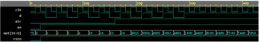
シフト レジスタが有効になっている時間は、以下のログで緑色で強調表示されています。方向を変える時間は黄色で強調表示されます。データ入力ピンが一定のままである時間は青色で強調表示されます。
シミュレーションログncsim> run rstn=0 data=1, en=0, dir=0, out=xxxxxxxxxxxxxxxx rstn=0 data=1, en=0, dir=0, out=0000000000000000 rstn=1 data=1, en=1, dir=0, out=0000000000000000 rstn=1 data=0, en=1, dir=0, out=0000000000000001 rstn=1 data=1, en=1, dir=0, out=0000000000000010 rstn=1 data=0, en=1, dir=0, out=0000000000000101 rstn=1 data=1, en=1, dir=0, out=0000000000001010 rstn=1 data=0, en=1, dir=0, out=0000000000010101 rstn=1 data=1, en=1, dir=0, out=0000000000101010 rstn=1 data=0, en=1, dir=0, out=0000000001010101 rstn=1 data=0, en=1, dir=1, out=0000000001010101 rstn=1 data=1, en=1, dir=1, out=0000000000101010 rstn=1 data=0, en=1, dir=1, out=1000000000010101 rstn=1 data=1, en=1, dir=1, out=0100000000001010 rstn=1 data=0, en=1, dir=1, out=1010000000000101 rstn=1 data=1, en=1, dir=1, out=0101000000000010 rstn=1 data=0, en=1, dir=1, out=1010100000000001 rstn=1 data=1, en=1, dir=1, out=0101010000000000 rstn=1 data=1, en=1, dir=1, out=1010101000000000 rstn=1 data=1, en=1, dir=1, out=1101010100000000 rstn=1 data=1, en=1, dir=1, out=1110101010000000 rstn=1 data=1, en=1, dir=1, out=1111010101000000 rstn=1 data=1, en=1, dir=1, out=1111101010100000 rstn=1 data=1, en=1, dir=1, out=1111110101010000 Simulation complete via $finish(1) at time 430 NS + 0
Verilog