


MEMSベースのセンサーデバイスにおける作動および検知メカニズムのレビュー
要約
過去数十年にわたって、微小電気機械システム(MEMS)デバイスの進歩は、経済的に小型化されたセンサーを製造技術と統合するために非常に要求されています。センサーは、複数の物理入力を検出して応答し、それらをアナログまたはデジタル形式に変換するシステムです。センサーは、これらのバリエーションを、デバイス変数を監視するためのマーカーとして利用できる形式に変換します。 MEMSは、その小さな寸法、低消費電力、優れた性能、およびバッチ製造により、小型化センサーで優れた実現可能性を示します。この記事では、MEMSベースのデバイスに対応できる標準的な作動およびセンシングメカニズムの最近の開発について説明します。これは、現在の時代のほぼ多くの製品カテゴリに革命をもたらすと期待されています。作動、検知メカニズム、および実際のアプリケーションの特徴的な原理についても説明しました。 MEMSベースのデバイスの作動および検知メカニズムを正しく理解することは、斬新で複雑なアプリケーション設計の効果的な選択において重要な役割を果たすことができます。
はじめに
センサーとアクチュエーターはまとめてトランスデューサーと呼ばれ、信号または電力をあるエネルギードメインから別のエネルギードメインに変換する機能を果たします[1、2]。さまざまな変換機器が、物理信号を電気信号(つまりセンサー)に変換します。さらに、出力信号は、電気信号を物理信号(つまり、アクチュエーター)に変換するのと同じように、集積回路(IC)を使用して電子システムによってさらに処理されます[3]。特に、センサーは、物理現象(つまり、振動、圧力、および流れ)または組成の変化(電気伝導率および潜在的な水素(pH))を検出および監視するデバイスです。センサーは変動を特定の形式に変換し、測定された変数をマークまたは制御するために利用できます[4、5]。一方、アクチュエーターは機械的な動きと力/トルクを生成するために利用されます。言い換えれば、感知は知覚をもたらすエネルギー伝達プロセスとして広く定義することができますが、作動は行動を生み出すエネルギー伝達プロセスです。センサーは3つの部分で構成されています。物理的および化学的量を検出するための検出要素、検出されたパラメータを電気信号に変換するためのトランスデューサ、変換された信号を読み取って解釈するために使用されるコンピュータなどの読み取りデバイス。
センサーの性能は、感度、分解能、精度などのさまざまな特性パラメーターによって評価されています。一方、感度は、対象物質濃度の最小値を決定します。分解能とは、測定された最大の大きさと、決定できる最小の部分との比率を指します。同時に、精度は絶対標準に対する測定の不確かさの量として定義され、センサーの定性分析に直接影響を与える可能性があります[6]。一方、検出限界(LOD)は、センサーによって識別できる物質の最小量であり、特定の物質を識別するセンサーの機能です。さらに、応答時間は、センサーが警告信号を生成するときに濃度が特定の限界に達する特定の時間であり、回復時間は、検出プロセス後、ベースライン状態を回復および復元するのにかかる時間です。
過去数十年の間に、マイクロエレクトロニクスデバイス製造技術の進歩により、説得力のある正確で高性能なデバイスシステムが生み出されました。テクノロジーは、人間の目には見えないほどデバイスを小さくできるようになるまで絞り込まれています。微小電気機械システム(MEMS)には、モデルをセンサーまたはアクチュエーターとして表すことができる小さなデバイスの革新が含まれます。 MEMSの分野での継続的な開発は、最適化されたコスト削減の小型化された電子機器の可能性を秘めています[7、8、9]。 MEMSデバイスの一般的な寸法は、通常、数十または数百ミクロンで測定されます。同じ製造方法を利用することは、マイクロプロセッサを構築するようになります。現在、センサーとアクチュエーターは、マイクロプロセッサーチップを使用して同様のスケールレベルで構築できます。最近の開発では、圧力、温度、慣性などのマイクロスケールのバッチ製造で、同様のチップハンドリングユニットを使用したバッチスケールのセンサーが実証されています。システムをチップに正確に重ね合わせると、複雑なシステムの操作が可能になります[10、11]。
MEMSは、半導体材料を使用して製造され、機械部品、センサー、アクチュエーター、および電子要素を、数ミリメートルからミクロンゲージまでの特徴サイズを持つ一般的なシリコン基板に組み込んだ技術です[12]。これらのシステムは、マイクロスケールで検知、制御、および作動する操作を実行できます。これは、個別にまたはバルクで操作して、マクロスケールに影響を与えることができます。 MEMS技術は、典型的な金属酸化物半導体デバイスへの典型的なSiウェーハ上のマイクロエレクトロニクスとマイクロマシニング技術の組み合わせを検討しました[13]。最近、MEMS技術は、さまざまな種類の自然センサーやアクチュエーターを認識するために大幅に成長しました。さらに、低電力定格[14]、迅速な応答、機械的手段でのアレイ製造、容易さ、安価、およびより優れた感度により、多くのアプリケーションで小型化されたセンサー製造に利用されています。重要なことに、検知材料の表面積対体積比が大幅に増加し、最終的に金属酸化物ベースのセンサーの動作温度が低下し、膨張材料の需要が増加しました[15、16、17]。
最近、二酸化チタン(TiO 2 )などの金属酸化物ベースのセンサー )、二酸化スズ(SnO 2 )および酸化亜鉛(ZnO)は、ガスを検出するための最も魅力的なタイプのセンサーになりました[18]。金属酸化物半導体(MOS)技術の動作原理は、検出中に分析対象ガスにさらされたときのアクセプター材料として使用される金属酸化物半導体の抵抗率の変化に依存します[19]。ただし、これらのセンサーの高感度は、高い動作温度でのみ達成されます[20]。さらに、選択性の問題もあります。別のアプローチは、それを他の検知コンポーネント、特に貴金属ナノ粒子(すなわち、Au、Ag、Pd、およびPt)と組み合わせて、化学的および電子的増感の極端な特定の利点のために、上記の障壁を克服することです[21,22 、23]。
MEMSデバイスは、MUMP(マルチユーザーMEMS)手順を介してMEMSCAPUSで製造できます。 MUMPsは、産業および学術研究にアイデアMEMS作成の実用的な証拠を提供する利益を生み出すプログラムです。全体的なMEMSCAPは、MUMPパッケージの重要な側面として3つの標準手順を提供します。3層ポリシリコン表面微細加工手順として説明されるPolyMUMP、電気めっきニッケル手順であるMetalMUMP、およびシリコンオンインシュレータ微細加工手順で提示されるSOIMUMPです。 [24]。 MEMS手順は、半導体デバイス製造の独自の技術である材料層の堆積、パターニング、エッチングから発展しました[7、25]。おたふく風邪の製造技術のステップは、デザインハンドブックのルール[24]に示されています。製造技術にもかかわらず、MEMSセンサーは、産業および家庭用アプリケーションの計装または人間の快適性の問題として広く使用されています。さまざまなアプリケーション分野(内部使用から屋外利用まで)でのMEMSセンサーの動作条件が多様であるため、さまざまな動作原理とさまざまなセンサー材料に基づいて、さまざまな種類のMEMSセンサーがモデル化されています。 MEMSセンサーは、湿度センサーや有毒ガスセンサーを含むガス検知システムに不可欠です[19]。
MEMSは広い領域であり、センサーやアクチュエーターとして、私たちの現在の生活の各側面をほぼカバーしています。小型化された形のほぼすべての製品カテゴリーを含む、電子マイクロシステムの新たな領域。これは、製造および統合プロセスにおける作動および検知技術の分野での急速な発展に貢献しています。対象となるアプリケーションの有効性は、特定のアクチュエータの適切な選択に大きく依存します。さらに、アクチュエータの基本的な効率は、電力と制御方法、互換性、必要なパッケージングの程度、費用対効果などのさまざまな要因によって異なります。この記事では、これらの主要な要因に対処しながら、この新たな分野の進歩を促進するために、多くの一般的な変換形式に重点を置いて、機能アプリケーションについて調査されたMEMS作動およびセンシング技術の徹底的な分析を提供します。残りの論文は次のように配置されています。セクションIIでは、微小電気機械システムを紹介します。セクションIIIでは、作動メカニズムの簡単なレビューを示します(MEMSデバイスを作動させるためのさまざまな原理とアプローチには、静電、電熱、電磁気、および圧電作動が含まれます)。セクションIVでは、ピエゾ抵抗、容量性、および光のセンシングメカニズムを含むセンシングメカニズムの概要を紹介し、セクションVでは、MEMSベースのデバイスの展望についてさらに説明し、最後に、セクションVIで結論と将来のトレンドを示します。
微小電気機械システム
今日MEMSテクノロジーとして知られているものが最初に登場したのは、1954年4月1日、スミス(1954)がベル研究所で物理レビューとして論文を発表したときまでさかのぼることができます。これは、ピエゾ抵抗と呼ばれる、シリコンとゲルマニウムの応力に敏感な効果のいくつかの最初の説明です[26]。小型化されたデバイスやシステムの巨大な拡張性と品揃えのために、MEMSは特に合理的な主要な略語ではありません(つまり、この分野はマイクロ、電気、機械システムだけではありません)。それにもかかわらず、略語MEMSは、フィールド全体(つまり、IC以外のマイクロマシニングから生じるすべてのデバイス)を示すために最も一般的に使用され、米国では微小電気機械、微小電気機械、またはマイクロエレクトロニクスおよびMEMSとも呼ばれます)[3] 。この小型化の一般的な領域の異なる名前には、ヨーロッパで有名なマイクロシステムテクノロジー(MST)[27]と、アジアで有名なマイクロメカニックス[28]が含まれます。 MEMSデバイスは、周囲の環境からの情報を測定し、それを有用な電気信号に変換するために、幅広いドメインを含みます。関心のある6つの主要なエネルギー領域があります:
- 1。
電気領域(電界、電流、電圧、抵抗、電荷、静電容量、インダクタンス、誘電率、分極、周波数を含む)
- 2。
化学ドメイン(組成、反応速度、濃度、pH、酸化または還元電位を含む)。
- 3。
機械的領域(長さ、幅、面積、速度、加速度、質量流量、体積、力、圧力、トルク、音響波長、音響強度などのすべての時間微分を含みます)。
- 4。
熱領域(温度、流れ、熱、比熱、エントロピー、物質の状態を含む)。
- 5。
放射領域(強度、位相、偏光、波長、反射率、透過率、屈折率を含みます)。
- 6。
磁区(磁場強度、透磁率、磁束密度、磁気モーメントを含む)。
これらのエネルギー領域とその中で一般的に遭遇するパラメータを(表1)に要約します。システム内の総エネルギーは、いくつかのドメインで共存でき、適切な状況下でさまざまなドメイン間でシフトする可能性があります[1,29]。
<図>設計されたチップの動作に応じて、MEMSはさまざまなカテゴリに分類できます。危険ガスの測定、監視、検出のための検知を実行するために使用できます。別の分類は、MEMSを、体に作用する、または流体のような体の材料と作用する、または薬物送達システムで使用されるデバイスなどの体外で作用するアクションタイプのデバイスとして使用することです。 MEMSデバイスは、コアアプリケーション領域(図1)に基づいて、流体、無線周波数(RF)、光学、およびバイオMEMS [10、30、31、32、33]を含む4つの異なるカテゴリに組み込まれています。
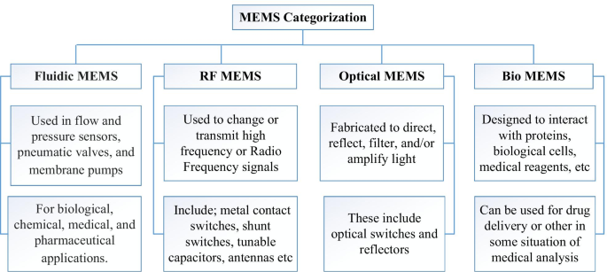
MEMSデバイスの分類
現在の技術のほとんどで、MEMSセンサーは、家庭用電化製品から航空産業に至るまで、多くの実用的なアプリケーションに適した新しい分野です。 MEMSの最も重要な特徴は、半導体チップの電気部品と効果的に通信する機能であり、センサー業界は、電子機能と機械的動作を組み合わせることにより、MEMS技術を使用して革命を起こしました[34]。小さいサイズに[35、36]。 MEMSベースのセンサーデバイスには多くの利点があり、さまざまなアプリケーションで重要な役割を果たします。これらの利点には、アレイ製造の可能性による低コスト[37、38]、低消費電力[37,38,39,40]、および小型サイズ[38,39,40,41,42]が含まれます。また、MEMSには、軽量、高解像度、安定したパフォーマンス、他のデバイスやシステムとの統合の容易さなど、他にも多くの利点があります。マイクロメカニカルからマイクロメカニカルデバイスへの削減は、慣性センサー、化学センサー、インクジェットプリンター、ジャイロスコープ、衛星、RF通信、スマートフォン、圧力センサー、加速度計、生物医学機器[43]、軍事用途、運動および力など、いくつかの分野で改善されています。センサー[44]。さらに、製造プロセスの低コストとシンプルさは、商業生産において重要な役割を果たします[45]。
動作原理によれば、センサーデバイスは動作原理に基づいて2つのカテゴリに分類できます。デバイス動作の静的モードと動的モードです[46、47]。 MEMSデバイスが静的モードに基づいている場合、周波数信号は含まれません。また、表面吸着質量によりビームが偏向し、一時的に応力や構造変形が発生します。ピエゾ抵抗器の変化により、光学的に検出または検知することができます。特定の化学結合がデバイス表面で発生し、内部のナノメカニクスがMEMSビーム検出を曲げることがあります[46]。動的モードでは、デバイスの最適なパフォーマンスを得るには、機械的な共振周波数を刺激する必要があります。振動システムによって達成され、特定のシステムで最大共振を励起できる最大振幅は、共振周波数と呼ばれます。ここで、共振周波数は、ビームのばね定数とその有効質量という2つの主要なパラメーターの影響を受け、これらのパラメーターに従って変化します。これが、共振周波数の変化を検出手段として利用するための動作原理です。必要な感度と解像度を得るには、品質係数を高くする必要があります[48、49]。これらのメカニズムはMEMSベースのデバイスの動作と出力信号の検出の基礎であるため、これらのメカニズムを理解して比較する必要があります。
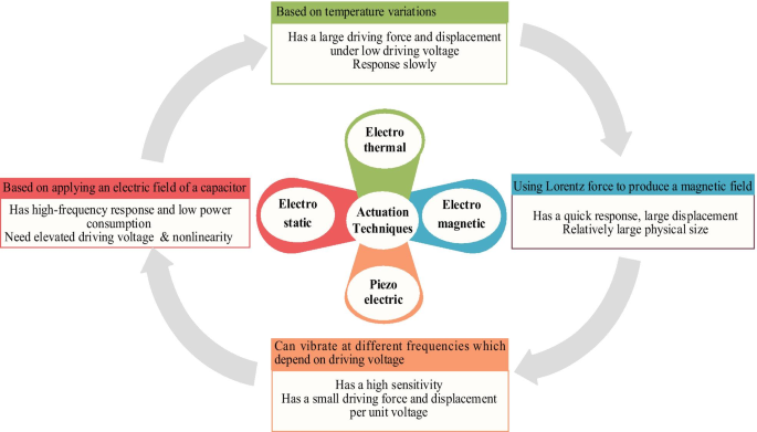
アクチュエーションテクニック
作動技術は、入力エネルギーを微細構造運動に変換するメカニズムに与えられた用語です。 MEMSデバイスを作動させるためのさまざまな原理とアプローチがあり[7、50、51、52、53、54、55]、その中で最も重要なものは次のとおりです。静電作動[56、57、58、59、60、61、62、 63,64]、電熱作動[4、44、65、66、67、68]、電磁作動[7、69]、および圧電作動[48、70](図2)。相補型金属-酸化物-半導体CMOS-MEMSセンサーデバイスは、平行平板コンデンサーを使用した静電作動またはマイクロヒーターを使用した電熱作動のいずれかで動作するように設計されています。一方、PolyMUMPsおよびMetalMUMPsセンサーデバイスは、埋め込まれたマイクロヒーターを使用して電熱作動を使用するように設計されています[71]。
MEMSベースのセンサーデバイスの作動技術
MEMSベースのデバイスは、正弦波力 F を適用することで作動させることができます。 ( t )、 前述の作動方法の1つを介して。 M 以降、式(1)を使用して一般的な運動方程式を求めます。 は天板の総質量 b は減衰係数、 k フレキシブルビームのばね定数
$$ M \ ddot {\ gamma} + b \ dot {\ gamma} + k \ gamma =F(t)$$(1)ここで F z での外部駆動力の振幅を表します -方向、\(\ ddot {\ gamma} \)\(\ ddot {\ upgamma} \)、\(\ dot {\ upgamma} \)\(\ dot {\ gamma} \)およびγ は、それぞれ質量の加速度、速度、変位です。
静電アクチュエータは非常に普及しています。応答時間が速く、消費電力が少ない[72]。一方、電熱原理を使用したアクチュエータが人気があります。それらは、低い駆動電圧の下で大きな駆動力と変位を持っています。電磁アクチュエータには、応答が速く、変位が大きいというメリットがあります。圧電原理を利用したアクチュエータは、駆動力や単位電圧あたりの変位は小さいものの、感度が高くなっています。したがって、これらの作動アプローチのいずれかを備えた高性能デバイスを入手するには、発生する原理を十分に理解することが不可欠です。
静電作動
静電作動の主な原因はコンデンサの電界であり、反対の電荷を持つ2つの平行なプレート間の引力に依存しています[12]。静電作動は、固定プレートと可動プレートの間に発生する特定の距離での2つの電荷間の相互力を表すクーロンの法則に基づいています。静電作動は、MEMSデバイスを作動させるための最も一般的なメカニズムの1つと見なされています。シンプルな設計、高速な応答時間、製造の容易さ、低消費電力を備えています。ただし、このタイプのアクチュエータの主な問題は、非線形性と駆動電圧の値の上昇です[72]。静電作動下でMEMSを研究する場合、いくつかのタイプの静電作動を注意深く検討する必要があります。最も一般的な形式は、2つの単純な平行板で構成されるコンデンサ、または複数の互いにかみ合うまたはかみ合わない指で構成されるコームドライブ構造に基づいています[72、73]。従来の方法[74]は、上部の可動プレートが特定の極性を持ち、下部の固定プレートが反対の極性を持つ平行プレート作動です(図3)。可動プレートの変位と振動は、2つのプレート間の電圧差に依存します。電荷の極性が類似している場合、固定プレートと移動プレートの間に反発変位がありますが、2つのプレートの電荷が異なる場合、移動プレートは固定プレートに引き付けられます。可動プレートの電荷の種類を定期的に変更すると作動します[50、56、74]。
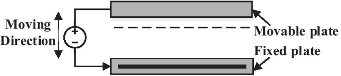
静電作動用の平行平板コンデンサ[75]
固定プレートがマイクロビームのすぐ下にあり、静止摩擦によってデバイスが崩壊するため、平行プレートが静電的に駆動される場合の主な問題の1つは引き込みの不安定性です[74、76]。コームドライブアクチュエータは、交互に配置されたフィンガー構造の2つのコームセットで構成されています(図4)。それらは通常、一方のコームフィンガーが固定されている基板と同じ平行プレートに配置され、もう一方は固定プレートに近づいたり離れたりするために柔軟な構造(スプリングなど)に接続されます[72]。可動コームと固定コームフィンガーの間に異なる電圧が印加されると、フリンジフィールドの静電力が固定外部正弦波力によって2つのコームを引き付けます。一般に、平行平板コンデンサは、アクチュエータの固定板と可動板の間のオーバーラップ容量が大きいため、単位面積あたりのコームドライブアクチュエータよりも強力です。ただし、設計者は、次の2つの主な理由により、アクチュエータをコーミングすることを好みます。それは、より大きな変位を生成し(数十マイクロメートルが利用可能)、力は変位とは比較的関係がありません。全体として、静電作動は、マイクロメカニカルアクチュエータ[77]、バイオセンサーアプリケーション[56]、湿度検知[57]、粒子および質量検知アプリケーション[50、78]、MEMSナノポジショニングシステム[58]、RFMEMSスイッチアプリケーション[ 13、79]、MEMS発振器の閉ループノイズ[60]、ナビゲーション(自動車グローバルポジショニングシステムGPS)[62、80]、ジャイロスコープ[81]、呼気中のバイオマーカー検出[82]および質量感受性ガスセンサー[82]。 63]。さらに、糖尿病の非侵襲的スクリーニングのための静電作動および容量性CMOS-MEMSベースのセンサーデバイスの理論モデルも報告されました。ここで、糖尿病のスクリーニングは、呼気中のアセトン蒸気(EB)の検出を通じて行われ、キトサンポリマーが検知材料として使用されました。具体的には、最適化された感度が約0.042、0.066、0.13、0.18、および0.26 pm / ppmと報告されました[83]。
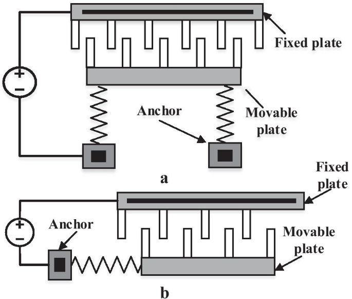
静電コームドライブ構成の概略図[84、85]、 a 縦方向のくし型アクチュエータ。 b 横方向アクチュエータ
MEMSデバイスを共振状態または振動モードに励起するには、固定子と回転子の2つのプレート間にAC電圧を印加して代替駆動を実行する必要があります。標準の運転モードは、次の[49]に従って示されています。単純な代替電圧( V 1 sin ωt) 、DCバイアス付きの交流電圧( V 0 + V 1 sin ωt) プッシュプル駆動(図5)。構造力をローターの両側に加えることができるため、プッシュプル駆動が一般的に最良の解決策と考えられています。プッシュプルは、コームドライブスキームに適した理想的なドライブです[49]。
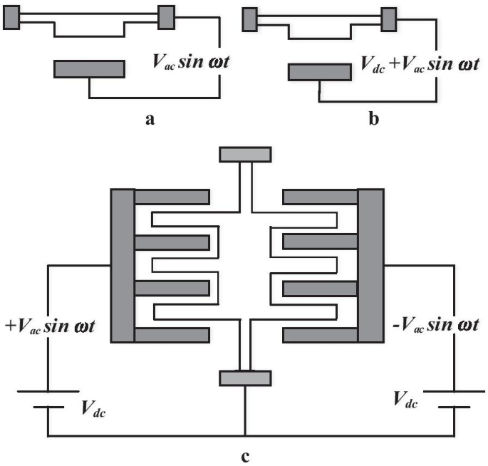
コーム駆動レゾネータ a シンプルな代替電圧駆動、 b DCバイアス付きの交流電圧、および c プッシュプル駆動方式[86]
電熱作動
電熱技術は主にMEMSドライブで利用されますが、センシングアプリケーションではほとんど利用されません[72]。電熱技術は、所望の変位を伴う動きを生成するための柔軟な構成に本質的に適切である。駆動は、異なる層の温度差への応答として生じる熱力のために、埋め込まれたマイクロヒーターの端子を介して適用されるAC電流によって伝導されます[66]。マイクロヒーターは、さまざまな材料層のコンポーネントで構成されており、高温で動作します。 AC電流が流れると、デバイスの温度が上昇します。異なる材料の熱膨張係数(CTE)の不一致により、材料が膨張し、熱応力が発生してデバイスが曲がります[72]。一方、冷却アプローチは、基板への伝導と周囲の空気(または液体)への対流によってアクセスできます。
[44、87]で報告されているように、これらの温度変化はデバイスに2つの影響を及ぼします。(1)デバイスの寸法変化またはデバイス内部で発生する応力、および(2)デバイスの材料特性は温度によって変化します。現在の技術は、マイクロヒーターに圧縮する必要があります。マイクロヒーターは、抵抗器に特定の電流を流すことで目的の熱を発生させるため、消費電力が低く、応答時間が短くなります。電熱力は(2)[88]で表すことができます。
$$ F_ {th} =\ alpha_ {T} AE(T-T_ {0})$$(2)ここでα T はCTE、 E はビームのヤング率 A はビームの断面積です。 T は最終温度であり、 T 0 は加熱前の初期温度です。マイクロヒーターの設計にはいくつかの材料が使用されています。たとえば、最高の性能、精度、広範な温度範囲、および安定性を実現するには、プラチナと金がマイクロヒーターの最良の決定事項になります[89]。ただし、コストがかかります[90]。 MEMSセンサーでマイクロヒーターを利用するには、生成された熱を有用な出力に変換するための内蔵温度センサーが必要です。温度センサーの場合、プラチナは−200ºC〜800ºCの温度範囲で利用でき、ニッケルは−100〜260ºCで利用できます[90]。報告によると、アルミニウムは温度検知にも適した材料です[91]。図6は、Uビームアクチュエータ(ホット/コールドアーム)、バイモルフアクチュエータ(バイマテリアルアクチュエータ)、および座屈アクチュエータ(Vビームアクチュエータまたはシャトルビーム)を含む電熱作動の一般的なメカニズムを示しています。
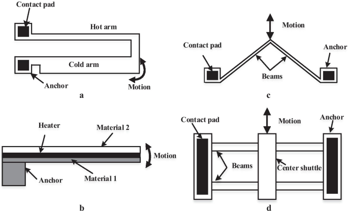
電熱作動の概略図 a Uビームアクチュエータ(ホット/コールドアーム)、 b バイモルフアクチュエータ(バイマテリアルアクチュエータ)、 c および d 座屈アクチュエータ(Vビームアクチュエータおよびシャトルビーム)[67、92]
Uビームアクチュエータはホット/コールドアームとも呼ばれ、アクチュエータはナローアーム(ホット)、ワイドアーム(コールド)アンカー、およびコンタクトパッドで構成されています[67、92]。これは主に、基板と比較して面内または水平方向の励起に使用されます。この手法の動作原理は、接触パッドに差動電圧を印加することに依存し、電流がアームを流れ、ホットアーム(高抵抗)はコールドアーム(低抵抗)よりも多くの電流密度を加熱します。したがって、幅の狭いホットアームは熱くなり、太いアームよりも膨張します。ホットアームは大きな熱応力を発生させます。両腕の間のこの差動ひずみにより、デバイス全体が変形します。
バイモルフアクチュエータは、バイマテリアルとも呼ばれ、2つの異なる熱膨張材料が結合して構成されています。最初の2つのアクチュエータとは異なり、バイモルフアクチュエータ[93]は通常、面外作動に使用されます。電流がビームを通過すると、材料の温度が上昇します。この温度では、熱膨張係数が異なるため、一方の材料で他方の材料よりも大きな膨張が発生し、熱応力とデバイスの曲げが発生します。
熱座屈アクチュエータは、Vビームまたはシャトルビーム[94]、アンカー、および接触パッドで構成されており、これらは主に面内または横方向の作動にも使用されます。電流がビーム間を流れると、発生するジュール熱によりビーム温度が上昇し、熱膨張が発生します。これにより、シャトルが膨張して移動したり、デバイスの中央のビームが最も単純で抵抗の少ない方向に押し出されたりする傾向があります。
実際の実装では、熱的に作動するMEMSデバイスの大部分は固有振動数に近い周波数で振動するため、デバイスの固有振動数を計算することが不可欠です。電子熱技術は、非常に低い励起電圧下での2層材料の熱膨張に基づく大きな駆動力と変位のために、より普及します。これは、同様の測定を使用する場合、他の戦略では達成できません[85、95]。電熱作動は、大きな変位[95]、製造の容易さ[72]、大きな力、および比較的低い印加電圧[52]などの複数の利点を示します。それどころか、それらは大量の電流と低電圧増幅器を必要とします。また、ジュール熱により消費電力が大きくなります。もう1つの制限は、周囲温度に対する感度です。最後に、電熱作動によって上昇する励起温度と熱は、システムのパッケージング段階とともに、隣接する電子機器にいくつかの欠点を引き起こす可能性があります[72]。
数多くのタイプの電熱作動が開発され、研究されてきました。ホット/コールドアーム[96,97,98]、バイマテリアルまたはバイモルフ[98、99]、および熱座屈アクチュエータ[98、100]。参考文献[101]は、バイモルフアクチュエータを使用した熱作動下でのマイクロカンチレバー振動を調査しました。参考文献[102]は、MUMPプロセスを利用して製造されたポリシリコンマイクロリング熱作動(RTA)の構造化された手順を提案しています。熱作動に基づくマイクロカンチレバーが設計されています。彼らは、システムが真空または流体(気体)液体であると想定し、分析ソリューションを提案しました[103]。デニス等。 [44]二酸化チタン(TiO 2 )を使用して湿度レベルを測定するために、比較的高温(40〜80°C)で動作するマイクロヒーターを内蔵した(CMOS-MEMS)システムを製造しました。 )センシング材料としてのナノ粒子。センサーは、電熱作動を使用して動的モードで動作し、出力信号は、ホイートストンブリッジ回路に接続されたピエゾ抵抗(PZR)センサーを使用して評価されました。 The humidity sensor output voltage rises from 0.585 to 30.580 mV as the humidity increases from 35% RH to 95% RH. The sensitivity of the humidity sensor increases linearly from 0.102 mV/% RH to 0.501 mV/% RH with an increase in the temperature from 40 to 80 °C and a maximum hysteresis of 0.87% RH is found at a relative humidity of 80%. In a further notable contribution, Almur et al. [104] modelled a MetalMUMPs acetone vapour sensing system based on electrothermal actuation and capacitive sensing. The output voltage change was found to increase linearly with increasing the acetone vapor concentration from 100 to 500 ppm with a concentration sensitivity of 0.65 mV/ppm. Due to the thick nickel layer of the MetalMUMPs technology used the device has very high mass (4.7 × 10 –8 kg) and low mass sensitivity (0.118 MHz/pg).
Electromagnetic Actuation
The electromagnetic operation has long been utilized in the sensing and driving of the large scaling applications (such as loudspeakers). This technique demands electricity to stimulate the magnetic effect. It uses the electromagnetic force (also can be called Lorentz force after the Dutch physicist Hendrik A. Lorentz 1895) to produce a magnetic field to the resonator by applying an alternating current on the coil or inductor integrated into the resonator (Fig. 7). Lorentz Force is defined as the force generated on a point charge as a result of the combined electric and magnetic forces on the charge [72]. Electromagnetic actuation has also been utilized as a guide to other actuation techniques, for example, electrostatic [33] and electrothermal [34]. In this technique, when a conductor conveying an electric current I can be applied to an external magnetic field B , this will induce a Lorentz force F L as stated by (3) [72].
$$\vec{F}_{L} =L\vec{I} \times \vec{B}$$ (3)ここで L indicted to the conductor length and × refers to the cross product operation. The current in the conductive element located within the magnetic field generates an electromagnetic force in a direction perpendicular to the current and the magnetic field. This force has a directly proportional to the current, magnetic flux density and length of the microbeam. Because of the interaction generated by the current between the magnet and the magnetic field, a mechanical displacement on the microbeam will be generated as a result of the applied current to the micro-coil. For example, electromagnetic actuation has been used to stimulate microbeam when being exposed to an external magnetic field by flowing current through the microbeam, as seen in Fig. 7a. Similarly, as alternating current flows through the device on the microbeam, this approach can be used to excite the out-of-plane resonator (Fig. 7b). Lorentz forces of equal value and opposite directions are produced if the coil is deposited on a structure of the microbeam. The opposite directions of the current flowing through the different parts of the coil correspond to these forces. Such forces balance one another out. Figure 7c, however, can induce a net motion that is used to actuate the microbeam [72].

Schematic of the electromagnetic actuation using Lorentz forces a in-plane actuator, b および c out-of-plane actuator [72]
The electromagnetic technique involves many merits over the other kind of actuation techniques. The main advantages of the electromagnetic actuation include the large displacement without the influence of the nonlinear effect [105], lower voltages due to they based on current rather than voltage-driven [7], in addition, they have a high reproducibility rate, they also have more features like rapid response, high accuracy, and the merit for controlling easily. For MEMS applications, the electromagnetic technique is the best choice to achieve maximum driving force for device size ratio [106]. However, they still suffering from some drawbacks due to using the huge current resulting in high power consumption, also their fabrication is complicated (normally be in need of inductive parts to produce magnetic flux also the possibility of including the manufacture of coils, and the deposition of a magnetic material) [7]. This fact combined with constructive difficulties has limited magnetic actuation applications. However, there are successful application examples in the literature as it may exist in MEMS switches devices [7], Optical switches, and micro scanners [69], gyroscopes [107], or relays [108]. Many researches are also based on magnetic actuation [109]. The magnetic microsensors utilizing the commercial 0.35 μm CMOS process has been investigated [110]. In a further contribution, Barba et al. [111] designed an electromagnetically actuated MEMS cantilevers proposed in order to minimize parasitic phenomena using Boron-doped silicon. In another seminal work, an electromagnetic and Piezoelectric actuated and piezoresistive sensed CMOS- MEMS device has been modelled for humidity sensing using ZnO NRs (6 μm/chitosan SAMs) as a sensing material [83]. The sensitivity was found to be 83.3 ppm [112].
Piezoelectric Actuation
Piezoelectric effect indicates the capability of a particular material to produce an electrical voltage in response to applied the mechanical stress. Piezoelectricity was discovered by the Curie brothers in 1880, and 'Piezo' meaning is coming from the Greek word that is mean 'press' or 'push'. A piezoelectric actuator defined as transducers that converts an applied potential into a mechanical movement or strain based on the piezoelectric influence [72]. Piezoelectric materials like quartz, zinc oxide, lead zirconate titanate (piezoelectric ceramic material PZT), and polyvinylidene difluoride (PVDF) are commonly used in sensor and actuator applications on a macro scale as well as in MEMS applications in recent years, but the sensing is limited due to their lack of a DC response [49]. Piezoelectric materials act electrically as insulators and required to be placed between two conductive electrodes so as to gather charge or to apply an electric-field (using an interdigitated electrode or sandwich structure) [113].
In MEMS devices, the basic principle of the piezoelectric actuation method is based on using a thin piezoelectric layer that is deposited as a part of the MEMS beam between flexible (Fig. 8). When a voltage is applied to the piezoelectric layer, the piezoelectric material expands according to the polarization of the applied voltage, which causes an axial bending across the length of the flexible beam [114].

Schematic of the piezoelectric actuator [72]
In general, piezoelectric actuators exhibit a lot of advantages such as high output force, good operating bandwidth, very compact size, lightweight, low power consumption, and fast response [114, 115]. Their characteristics are well known and have been used for decades. Most first sensors use piezoelectric actuation and are still in use today. However, small displacements of actuators are a major drawback, and their high-temperature sensitivity [72], nonlinear working area and hysteresis limit their wide range of applications [49]. Piezoelectric materials are very brittle. They can seldom be utilized alone but are often connected to a flexible structure for actuation and sensing applications. There are several works based on piezoelectric actuation [2, 48, 114, 116] studied the prospective to use a piezoresistive microcantilever for environment application, particularly for humidity sensing. Mahdavi et al. [117] proposed a new class of accurate dew point measurements taking advantage of thin-film Piezoelectric-on-Silicon (TPoS) resonators using ZnO NRs (6 μm/chitosan SAMs). The sensitivity was found to be 16.9–83.3 ppm at the range of response time of 46 s/167 s. sensitivity to mass loading based on piezoelectric excitation is investigated for chemical sensing [118, 119] reported piezoelectric transduction of flexural-mode silicon resonators to achieve efficient temperature compensation. The resonance gas sensor using piezoelectric MEMS for defence applications was reported [120].
Actuation Techniques Discussion
Different types of MEMS actuators require different drive electronics. As per mentioned in this article, there are different principles and approaches to actuate MEMS devices. The most important of which include:electrostatic actuation, electrothermal actuation, electromagnetic actuation, and piezoelectric actuation. Electrostatic actuators are a traditional field and considered one of the most popular mechanisms for actuating MEMS devices. They have a simple design, fast response time, ease of fabrication and low power consumption. However, the non-linearity and the elevated value of the driving voltage is the major matter of this type of actuator. Electrothermal actuators provide very low resistance to their drive sources and require high currents rather than high voltages to move them. High voltage amplifiers are not particularly suitable for use in electrothermal MEMS actuators. Instead, a low voltage and high current signal source are required. Of course, this can also work if the output current of the high voltage amplifier is large enough to drive the electrothermal actuator, but it is not a particularly energy-efficient or cost-effective solution. For MEMS applications, electromagnetic technology is the best choice to achieve maximum driving force per device size ratio. However, they still suffering from some drawbacks due to using the huge current that results in high power consumption, also their fabrication is complicated (normally be in need of inductive parts to produce magnetic flux also the possibility of including the manufacture of coils, and the deposition of a magnetic material). Piezoelectric actuators also required high voltage amplifiers, but since they are typically used for resonance, the drive requirements in terms of driving voltage are typically lower than those required for other actuators. The recent research of MEMS-based sensor devices which can be actuated using the four basic actuation techniques that have been used during the last few years for many applications, as shown in Table 2. It can be clearly observed that there is a rising development pattern in the field of micro-assembly and micromanipulation for MEMS-based sensor devices that have been categorized based on actuation techniques. Nowadays, a wide range of applications has been identified for MEMS-based sensor devices that provide high sensitivity and resolution. The sensing systems are getting more robust and reliable due to the integration configuration.
<図>Sensing Mechanisms for the Output Signal
The sensing mechanism is used to sense the output of the MEMS devices. The basic of the sensing technique is based on the use of a polymer deposited on the sensing layer of the device to absorb a particular chemical that creates a variation in the stress, mass, electrical or mechanical characteristics of the beam. To estimate the change in the mass, the resonant frequency of the device can be measured based on the detected mass increment that is one of its parameters. Then again, when the polymer absorbs the mass, piezoresistor that is situated on the surface of the sensing element can be used to estimate the mass of the beam. Another method of detecting suspected chemicals is to use thermocouples to measure temperature changes caused by the heat generated by the polymer absorbing analyte [49].
To sense the output of these MEMS devices methods such as piezoresistive, capacitive or optical mechanisms are used (Fig. 9) [123]. Different sensing mechanisms have different advantages and disadvantages at the same time.

Sensing mechanisms of MEMS-based sensor devices
For instance, optical sensing has good feasibility; however, it is very expensive to implement compared to capacitive and piezoresistive techniques [124]. Capacitive and piezoresistive techniques are the common methods used to sense the output signal. CMOS- MEMS device was designed to encompass both piezoresistive and capacitive sensing techniques due to the features of 0.35 µm CMOS technology used to design it. In contrast, PolyMUMPs and MetalMUMPs devices were designed to use only capacitive sensing techniques.
Piezoresistive Sensing
Piezoresistive is a common sensing principle used in MEMS devices. Essentially, the principle of piezoresistive materials is based on the resistance change when their strain changes in response to applied stress. This change can be observed in the electrical resistance of the material of the device as a consequence of a surface-stress change due to bending. The resistance value of the piezoresistor with the resistivity ρ of a resistor, length of l and cross-section area A is given by (4) [29].
$$R =\frac{\rho l}{A}$$ (4)The change ΔR in resistance is proportional to the applied strain can be defined in (5) [29, 125].
$$\Delta R =G\varepsilon R$$ (5)where G is the gauge factor work as a proportionality constant of the piezoresistor, ε is the strain in the material, and R is the piezoresistor resistance. A piezoresistive element behaves differently towards longitudinal and transverse strain component presented by [29]. According to (5), the resistance of a piezoresistor can vary owing to the changes of the geometry (length and cross-section) or in the property of the material (resistivity). Piezoresistive detection depends on the difference in resistivity of material when stress is applied. In a piezoresistive material, the change of resistivity because of the application of stress has a much greater effect on the resistance than the change in resistivity because of a change in the geometry (sensors rely on the change of resistance owing to the geometry are so-called strain gauges) [72]. (Fig. 10) shows different resistor orientations and external force loading directions [88].

a Longitudinal piezoresistance dominates, b および c transverse piezoresistance dominates presented [29]
The main drawback of this sensing mechanism is the solid temperature reliance of resistivity. To limit this impact, normally, a collecting of four piezoresistive designed is utilized to shape a Wheatstone bridge. This limits the temperature reliance [72]. Furthermore, the small changes in the electric signal generated from gauges are translated and gauged as voltages utilizing this Wheatstone bridge [49]. Wheatstone bridge utilizes four resistors arranged in the bridge of the four arms (Fig. 11). Based on the quantity of these active resistors (acting as a transducer), single active bridge (single transducer), half active bridge (double transducers), and the full active bridge (quadruple transducers) of the bridge of Wheatstone might be utilized as reported [72]. The single active bridge as well called Quarter Bridge that utilizes just a single active component which changes because of a physical ambient, for example, pressure, power, temperature, while the remnants of that resistors will be passive and so on. MEMS systems have been used as temperature, calorimeter, and in combination with the Wheatstone bridge, sensors allow the base fluctuations. Thermal bridge system is one of the best-known sensing platforms among MEMS. In the AC-driven Wheatstone bridge configuration (Fig. 11b), researchers have utilized the resistance-based thermometry to analyse temperature changes with micro-Kelvin resolution. In an overview, the right half of the bridge comprises a sensing resistor on the lower branch with associated resistance on the top, while the left side is defined as the matching one. Fixed resistors with a relatively low resistance coefficient of temperature are used with resistance values, which was chosen to enhance stability and resolution based on the previous study [126].

Schematic types of a Wheatstone bridge, a quarter bridge, b half-bridge, and c full-bridge configurations [72]
Silicon piezoresistor and polysilicon patches are generally utilized in MEMS sensors. The resistivity of silicon relies upon its strategy for doping. N-type doped with silicon is less sensitive than p-type. This raises limitation to the fabrications. In this situation, an in-plane transversal and in-plane longitudinal will be the most significant elements [72]. For semiconductor materials like silicon, the longitudinal and transverse gauge factors owing to geometry change are quite tiny compared to their values due to resistivity change, hereafter the change in geometry can be ignored, and the longitudinal and transverse gauge factors due to only the resistivity change are found using (6) and (7), respectively [127].
$$G_{L} =\pi_{L} E$$ (6) $$G_{T} =\pi_{T} E$$ (7)ここで E is Young's modulus of the piezoresistive material. π L and π T are the longitudinal and transverse piezoresistance coefficients, respectively, for arbitrarily oriented polysilicon grains, and their values are given in Table 3 [19].
<図>Currently, the piezoresistive effect has been utilized as a bio-or chemical detection [48], humidity sensing purpose [4], switch applications [59], biomarker detection in exhaled breath [82], micro scanners [69], pressure sensing [128], and mass-sensitive gas sensors [63]. Zope et al. [117] developed a resistively sensed thermally-driven piezo resonator composed predominantly of CMOS material for mass sensing applications. whereas mass sensitivity of 24.96 kHz/ng was reported. The extracted mass resolution of 16.3 fg have also been observed, hence showing great potential to serve as an aerosol sensor).
Capacitive Sensing
The capacitive sensing mechanism is based on measuring the changes of the capacitance between the stator and rotor fingers or between the fixed plate and movable plate [88]. Capacitive sensing is the main dominant method for micromachined applications due to its compatibility with all the fabrication approaches and stiffness [129, 130]. Capacitive sensing has many attractive features include high sensitivity, low power consumption, simplicity in design, low drift and low-temperature dependency. Furthermore, the measurement of the output signal can be easily fabricated on the PolyMUMPs die using capacitive sensing. Only a single parallel plate can be used to capacitively sensed the variations in the natural frequency or amplitude of the MEMS devices (such as a CMOS-MEMS device and a PolyMUMPs device) or by applying a comb finger (such as a MetalMUMPs device).
For CMOS-MEMS device and PolyMUMPs devices, when there is no actuation (Fig. 12a), the initial static sensed capacitance (Cs0 ) between the lower fixed plate and the movable top plate is calculated using (8) [19].
$$C_{s0} =\frac{{\varepsilon A_{s} }}{{z_{0} }}$$ (8)where ℇ is the relative permittivity of the dielectrics, As is the area of the sensed plates and z0 is the gap between the fixed and movable plates. When the movable plate is displaced by z (Fig. 12b) the initial gap changes, and hence the capacitance will change too, and it is found by (9).
$$C_{s} (z) =\frac{{\varepsilon A_{s} }}{{z_{0} - z}} =C_{s0} \frac{{z_{0} }}{{z_{0} - z}}$$ (9)
Parallel plate capacitor showing a initial condition and b after displacing the movable plate [19]
At the same time, for the MetalMUMPs devices, the output can be detected capacitively by utilizing the differential comb fingers design. As appeared in Fig. 13, there are two arrangements of fixed comb fingers to have the differential capacitance.

Comb fingers configuration for MetalMUMPs device showing a the initial condition and b the displacement of the vibrating comb finger [19]
For the initial condition, when the device is not actuated (Fig. 13a), the static detected capacitance C0 for every set of vibrating-fixed fingers could be calculated by (10).
$$C_{0} =n\frac{{\varepsilon l_{f} w_{f} }}{d}$$ (10)where l f and w f are length and width of the overlapping area of the vibrating and fixed comb fingers, respectively. d is the gap between the fixed and vibrating comb fingers and n is the number of the vibrating comb fingers. When the device is moved by y toward the fixed comb finger one as appeared by (Fig. 13b), the capacitances C 1 および C 2 will be changed and relying upon that shift, and their values can be calculated using (11) and (12), respectively.
$$C_{1} (x) =n\frac{{\varepsilon l_{f} w}}{d - y}$$ (11) $$C_{2} (x) =n\frac{{\varepsilon l_{f} w}}{d + y}$$ (12)The output signal of the device will be measured as a voltage due to change in the sensing capacitance upon actuation using MS3110 capacitive readout circuit that translates the change in capacitance to the output voltage change in response to the temperature of the microheaters. Nowadays, capacitive effects are used in MEMS resonators [60], biosensor application [56], humidity sensor [57], diabetes screening [66], Navigation (automobile Global Positioning System (GPS)) [62], a low noise accelerometer [131], and RF MEMS capacitive switches [132].
Optical Detection
Optical sensing mechanism depends on detecting the changes in the transmitted light compared to the received light. The detection of compound species by spectral transmission strategy is broadly acknowledged. Optical sensors are notable due to their selectivity since it does not rely upon any chemical reaction or any chemical catalyst activities. Air pollutants identification is recognized by using the characteristics of the optical species (for example, absorption, refractive index, Raman scattering, fluorescence, and reflection). Optical sensors utilize emission and absorption measurements primarily through different technologies such as Fourier transform infrared spectroscopy (FTIR), surface plasma resonance (SPR), differential optical absorption spectroscopy (DOAS), laser diode absorption spectroscopy (LDAS), cavity ring-down spectroscopy (CRDS), non-dispersive infrared (NDIR) spectroscopy, light detection and ranging (LIDAR), UV fluorescence and chemiluminescence for the sensing of air pollutants in air specimens. Normally, the light will be cross through, modified or reflected by some space having the relevant medium (Fig. 14). Beer–Lambert law can be used to govern the optical detection of the air pollutants as per the following:
$$I =I_{0} *e^{ - \alpha l}$$ (13)where the transmitted light through the specimen is I 、私 0 is the received light, α represent the absorptivity, l represents the length of the path.

Schematic representation of an optical MEMS sensor [133]
However, the majority of the applications for optical MEMS are in communications; there are various uses in different fields [134]. The literature covered numerous attempts to introduce the optical detection of air pollutants. A few of these sensors are used to recognize chemicals. This displays the multifunctional part of these sensors. Infrared spectrometry is a case of a technique that can be utilized for optical sensing [135]. In a further notable contribution, Huang and co-workers have also demonstrated [136] the simulation of an integrated optical MEMS accelerometer. The effective simulation results have demonstrated as follows:a resonance frequency of 562.85 Hz, a mechanical sensitivity of 781.64 nm/g, an optical system sensitivity of 1.23, a resolution of 1.037 µg, and low cross-sensitivity. The proposed accelerometer can be used for improvements in MEMS inertial navigation devices. Another model is the Fabry–Perot optical sensor [137]. Basically stated, the principles of this sensor are based on bringing gas into a chamber and a short time later going light through the chamber. Due to changes in the substance piece, the light experiencing will be not exactly equivalent to without the gas. This light is broke down, and from the results, confirmation can be made about the sort of gas being tested. The fruitful testing of an optical MEMS sensor for the location of catechol was reported [133]. The absorbance measurement of catechol oxidation was performed by blue light (472 nm) attached through a MEMS device. The light was transmitted from a free-space blue laser working in persistent wave mode and is focused on a multimode fibre utilizing manually arranged to organize. Received light was coupled by means of the optical fibre to a USB connected spectrophotometer which assisted computerized information collection utilizing the software.
Sensing Mechanisms Discussion
In view of different working principles, the above-mentioned sensing mechanisms can be divided into three types, namely piezoresistive, capacitive and optical mechanisms. There are benefits and drawbacks for different sensing mechanisms at the same time. For instance, optical sensing has good feasibility; however, it is very expensive to implement compared to capacitive and piezoresistive techniques. As a result, piezoresistive and capacitive techniques are the common methods used to sense the output signal. Any small change in the stress could be detected using a piezoresistive technique. A main disadvantage of the piezoresistive sensing technique is the high-temperature reliance of resistivity. In Table 3, present the recent work and progress (last 5 years), including actuation and sensing mechanisms, sensing materials, fabrication technology and application. The miniaturized microchip presented (in Table 4) can be utilized for gas and humidity sensing, human health screening, inertial navigation with good repeatability, high resolution, high sensitivity, and rapid response. In addition, MEMS sensors have been proven to be an effective medium for sensors combined with on-chip electronic circuitry. It can therefore function not only as a portable sensor chip but can also be linked as part of the Internet of Things (IoT) network to achieve real-time and remote high-sensitivity moisture tracking.
<図>Discussion
Recent developments are about new technologies that can harvest energy from the environment, because sustainable self-sufficient micro/nano power sources are an emerging field of nanoenergy, which involves nanomaterials and nanotechnology when harvesting energy for powering micro/nano systems [139]. The triboelectric charge is produced only on the surface dependent on the physical friction between two separate materials. The triboelectric nanogenerator (TENG) is a device that transforms mechanical energy into contact separation or relative sliding between two materials with opposite polarities. TENG based on the coupling effect between triboelectricity and electrostatic induction in which it’s updated progress and potential applications as new energy technology and as self-powered active sensors. The suggested approach uses biomechanical energy transfer to electricity from human activity [139, 140]. Amongst them is a successful study has been investigated for the conversion to wearable energy from portable biometric devices and self-powered sensors based on triboelectricity (i.e. the charge produced on the touch surface) [141,142,143,144].
-
To decrease power consumption during operation, sensors of woken up or almost zero-power supplement need to proposed and investigated, meaning that these sensors do not have any energy consumption. With these components of MEMS, MEMS sensors can work for a long period or can be operated in a self-powered.
-
Looking forward to the future-oriented sensors, sensors with flexibility have become hot topics of the recent research in the latest years owing to their versatility and great prospective in health/human beings applications. Flexible sensors are often used in combination with wearable sensors to have their unique advantages. More than just utilizing the flexible sensor such as a wearable electronic for observation functions, they can be even utilized as a human–machine interface for achieving higher requirements. With the enhancement of the quality of human life, wearable devices and human–machine interfaces have been recognized as important directions for developing sensors of the future with sufficient flexibility and versatile sensing capabilities. Wearable electronic devices can be simply integrated with the human body to extend our perception capabilities. Sensor functions of wearable electronic devices include, but are not limited to, force, strain, electrophysiology, heart rate monitors, temperature, fitness trackers, etc. With the service of various devices among different anatomical positions, development of many applications of the human body sensor can be facilitated from hospital care to fitness and wellness tracking, human–machine interfaces and recognition and assessment of cognitive states.
-
Meanwhile, by combining MEMS sensor with artificial intelligence (AI), the next generation of sensors will provide clear evolutionary impact and help humans interact with other things in various applications circumstances. Moreover, the quick improvement of the modern community has observed the expanding association among people with machines, demanding huge intelligent human–machine devices. Around a huge data and hypersensitive detecting, MEMS sensor utilizing a machine learning strategy dramatically stimulates the enlargement of the coming generation smart sensing system. This interactive system with next-generation sensor provides consumers with a more comprehensive experience. It can be used for many practical applications, such as simulation of sports training, entertainment, medical rehabilitation and so on.
Conclusions and Future Trends
It is well recognized that MEMS-based sensors play a key role in the field of miniaturization and electronic microcircuits. It is necessary to understand and compare these mechanisms since they are the basis of the MEMS-based devices operation and output signal detection. This article reviews several popular actuation and sensing mechanisms related to MEMS devices that have emerged over the past few decades. This article introduced a descriptive overview to the advancement of the actuation and sensing mechanisms of the MEMS-based sensor devices. The up-to-date trends and the restrictions while giving a valuable perception into the field of emerging actuation and sensing technologies. A comprehensive discussion was presented, underlining the significance of the actuation and sensing mechanisms, its structure, working principles, classification, fabrication and applications. Proper understanding of the actuating and sensing mechanisms for the MEMS-based sensor devices play a vital role in their selection and effective application in various innovative technologies. In addition, the proper selection of actuating and sensing techniques in MEMS sensors based on the desired application such as sensitivity, resonant frequency, input\output voltage, temperature etc., will lead to fast-commercialization and better product stability.
In order to perform various tasks for different applications such as industry and electronic equipment, different MEMS devices with different structures collaborated with diverse actuation and sensing mechanisms will arise in true-life. Moreover, MEMS devices will not only be used for simple tasks, but also for more jobs that are complex. At the same time, MEMS devices will have greater freedom and can meet the needs of a variety of applications. However, in order to pursue higher accuracy and miniaturization, the complexity of MEMS device design will continue to increase. In addition, MEMS products have a close relationship with the market. It can be predicted that MEMS devices will realize more functions, miniaturization and low cost, which is a huge challenge for other products. Therefore, in the next few years, MEMS fabrication approaches will develop to a higher level to meet market demand. With the advancement of MEMS device fabrication processes, unique hardware makers will seek after shorter fabrication cycles and quicker fabrication speeds.
One of the central areas of the future trend in this area is reliability research and improvement methods. Moreover, new materials and cost-effective of the fabrication techniques will provide important opportunities for development. It has been demonstrated that the design capability is not limited to standard principles and can improve qualitative performance. Despite MEMS advantages, few challenges still exist in the following aspects.
-
The traditional MOS thin films by MEMS techniques often show poor sensitivity to target gases due to the compact surface structure and low crystallinity.
-
In recent studies, it have tried to integrate high-performance MOS nanomaterials onto microheaters. Still, it is difficult to control and cast the slurry-based MOS nanomaterials onto the suspending heating area of microheaters. However, the low yield and large device-to-device deviation hamper the sensor fabrication on a large scale.
-
It is also complicated to improve the adhesion between microheaters and sensing materials to get stable parameters, especially at high temperatures > 350 °C which results in decreased sensing performance and low stability [14, 145].
-
Fabricating sensing films with high sensitivity using MEMS compatible methods is an urgent goal.
-
Towards a new era, different challenges can face MEMS-based sensors in terms of power supply and intelligence during the operation, such as the challenges of the flexibility of wearable applications, the friendly interactive capabilities of human–machine interface applications, and analysis of the huge data.
データと資料の可用性
該当なし。
略語
- MEMS:
-
Microelectromechanical system
- pH:
-
Potential hydrogen
- IC:
-
集積回路
- LOD:
-
検出限界
- MUMPs:
-
Multi-user MEMS
- MST:
-
Microsystems technology
- RF:
-
Radio frequency
- CMOS:
-
相補型金属酸化膜半導体
- CTE:
-
The coefficient of thermal expansion
- AC:
-
交流
- DC:
-
直流
- RTA:
-
Ring thermal actuation
- PVDF:
-
Polyvinylidene difluoride
- GPS:
-
Global positioning system
- FTIR:
-
フーリエ変換赤外分光法
- SPR:
-
Surface plasma resonance
- DOAS:
-
Differential optical absorption spectroscopy
- LDAS:
-
Laser diode absorption spectroscopy
- CRDS:
-
Cavity ring down spectroscopy
- NDIR:
-
Non-dispersive infrared
- LIDAR:
-
Light detection and ranging
- IDE:
-
Interdigitated electrodes
- PZR:
-
Piezoresistive
- EFS:
-
Electrostatic field sensor
- AI:
-
Artificial intelligence
ナノマテリアル