


ブレッドボード PCB プロトタイプから完全な製品への移行ガイド
ブレッドボード PCB プロトタイプからのスケーリングは、創造性と手順を組み合わせた複雑なプロセスです。開発のタイムラインは、プロジェクトの実行者と同じくらい個人的なものであり、すべては常に作成者の手に委ねられています。ただし、途中で探すべきマイルストーンがいくつかあります。ブレッドボードPCB
https://youtu.be/HAOvEPh8hms
PCB プロトタイプの構築を開始する
これで、この素晴らしいアイデア、または PoC (概念実証)ができましたが、大量生産する価値のあるものにスケールするか、少なくとも一部のメーカーがデモ目的で製造できるようにする必要があります。 PCB プロトタイプの構築をどのように開始しますか?
ハードウェア設計では、PCB プロトタイプは、設計者が設計を視覚化してテストするのに十分な、製造された (簡単に複製可能な) 製品を表す「手作り」のモデルです。プロトタイプという言葉は、ラテン語の proto (オリジナルを意味する) と、types (形またはモデルを意味する) に由来します。
すべてのチュートリアルが公開されており、多数の無料リソースが利用できるため、ほとんどの人が数時間で PCB プロトタイプを迅速に作成できるようになりつつあります。 PCB プロトタイプを商品化できる場所に持ち込むには、多くの労力、計画、およびある程度の専門知識が必要です。ハードウェアに関する多くの決定を行う必要があり、最終的にはデバイス ソフトウェアに関する決定が必要になります。ブレッドボードPCB
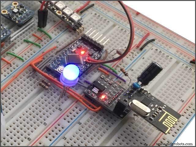
Raspberry Pi や人気の Arduino で簡単に構築できますが、これらで大量生産できる可能性はほとんどありません。もちろん、これは、Arduino Pro Mini のような Arduino ボード上にボードを構築できない、またはヘッドレス Arduino をプラグインして、そのようなものを製造し続けることができないという意味ではありません。それでも、非常に高価になる可能性があり、必要以上に強力になることさえあります.
今日のハードウェア スタートアップの多くは、最初の PCB プロトタイプを Arduino で構築しています。 . Arduino 電気工学のバックグラウンドがなくても、または必要なプログラミング スキルがなくても、簡単に習得できます。子供でもできますし、多くの子供ができます。
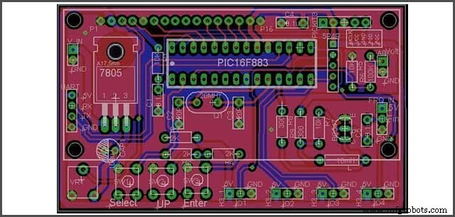
1.1 ブレッドボード PCB —コンポーネントの選択
PCB プロトタイプの作成を開始するための最初のステップは、必要なコンポーネントを知ることです。ブロック図または既存の PoC に基づいてそれらのアイデアをすばやく得ることができ、デバイスの必要な機能でさえもすぐにそれを伝えることができます。たとえば、ウェアラブル ハートビート モニターのようなものを構築する 以下のいくつかが必要になります:
1. マイクロコントローラ ユニット – Atmega、ARM、PIC など
2. 脈拍センサー – 専用の脈拍センサーが機能する場合もあれば、LED と光検出器の組み合わせも機能する場合があります。
3. 電源ユニット
4. ディスプレイ インターフェイス – LCD、LED、OLED、TFT など。
必要な部品のすべてではないにしても、単一の電子機器サプライヤから、場合によっては複数のサプライヤから、ほとんどの部品を簡単に外注することができます。以下は、AliExpress、Digi Key、Arrow、Mouser、Adafruit などから詳細を購入できるサプライヤーです。
1.2 回路図
次のステップは、通常、回路図と呼ばれる電子設計の図を作成することです または回路図。回路図は、すべてのコンポーネントがどのように接続されているかを示しています。これは手作業ではなく、この目的のために設計された独自のツールです。
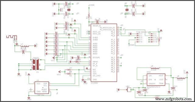
回路図の作成は、最終的なデバイスを構築するための重要なステップであり、スキップするわけにはいきません。スキーマを使い始めるのはとても簡単です。構築するための適切なツールを知る必要があります。回路図設計に使用できる回路設計ソフトウェアには、無料のものと有料のものがあります。ほとんどの設計ソフトウェアは、回路図の描画と PCB レイアウトの作成に使用できます。
使用するソフトウェアの一部を以下に示します:
1. KiCAD – 無料で使用できます。
2. Eagle CAD – プレミアムですが、無料オプションは限られています
3. アルティウム – プレミアム
4. DipTrace – プレミアム
5. OrCAD – プレミアムですが、無料トライアルを提供しています。
使用する設計ソフトウェアを決定したら、各ソフトウェアのルック アンド フィールが異なる可能性があるため、ソフトウェア環境に慣れることができます。
選択したソフトウェアで回路図を作成するときは、回路図設計の標準的な方法に従う必要があります。
いくつかの従来の方法を以下に示します –
1. ジャンクション ドットを使用して、ジャンクションで接続する複数の接続を示します。
2. 何百もの接続を描画するのではなく、ピンのネット名を使用します。これを行うと、不要な混乱を招くことなく、回路図の読みやすさが向上します。
3. 同じデバイスには常に同じ記号を使用する
4. 特に複雑な回路を設計する場合は、スキーマを論理ブロックに分割します。
回路図設計が完了し、完全にクロスチェックしたら、次のステップは回路設計を PCB の製造に変換することです。レイアウトの失敗の可能性が高く、最終製品の機能に悪影響を及ぼす可能性があります。ボードの製造には、いくつかの PCB レイアウトが使用されます。
次の章では、PCB プロトタイプ用のプリント回路基板の作成について説明します。
PCB プロトタイプ用のプリント回路基板の作成
PCB プロトタイプ用のプリント回路基板を作成します。まず、回路図を作成することは、本格的なプロフェッショナル ボードを作成するプロセスの 1 つのステップです。
スキップできないプロセスの次の段階は、プリント回路基板のレイアウトを設計することです。しかし、プリント回路基板とは何ですか?
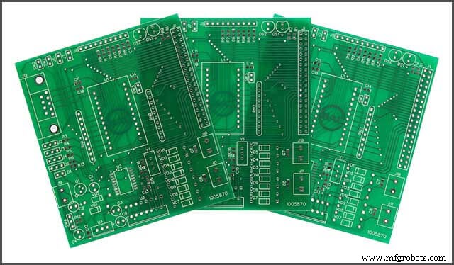

プリント基板 、別名PCBは、すべての電子部品を1か所に保持して接続する物理的なボードです。回路図設計は通常、いくつかの方法を使用して PCB に転送されます。 PCB の設計は、次のようないくつかの要因に影響します
1. コスト – 重要なボードほど、製造コストが高くなります。
2. パフォーマンス – ボードの設計と使用されるコンポーネントの種類は、デバイスの全体的なパフォーマンスに影響します。設計が不十分なボードはノイズの影響を受けやすく、デバイスのパフォーマンスが低下する可能性があります。
3. 耐久性
4. その他多数。
回路図の準備ができたら、PCB の作成に進みます。
PCB は、回路図の作成に使用されたのと同じソフトウェアで設計されています。
ソフトウェアは、指定されたコンポーネントと回路図に基づいて PCB レイアウトとフットプリントを生成します。回路図がないと、ソフトウェアは基本的な PCB レイアウトを作成しません。
PCB レイアウトの作成を開始することは、初めてのユーザーにとっては時間がかかり、面倒なことかもしれません。それでも、幸いなことに、ほとんどの PCB ソフトウェアについて、それらの構築方法を学習するためのいくつかの便利なチュートリアルとリソースがオンラインにあります。
選択したソフトウェアによっては、通常、ユーザーが回路図ビューから PCB が設計される PCB レイアウト ビューに切り替える方法があります。
最終的なデバイス モデルを想定して PCB を設計します。また、使用されているソフトウェアには、PCB レイアウトが使用されている PCB プロセスのデザイン ルールを満たしていること、および PCB が回路図と一致していることを確認するためのさまざまな検証ツールがあります。あなたのデザインがあなたのデバイスを壊すかどうか、すぐにテストできます。
製品が小さくなり、コンポーネントを密集させなければならないほど、PCB レイアウトの作成に時間がかかります。製品が大量の電力をルーティングしたり、ワイヤレス接続を提供したりする場合、PCB レイアウトはさらに重要で時間がかかります。
ほとんどの PCB プロトタイプ設計の重要な部分は、電源ルーティング、高速信号 (水晶クロックなど)、およびワイヤレス回路です。
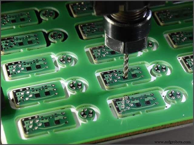
PCB プロトタイプの設計を補完したら、プリント回路基板の製造に進む必要があります。これを行うにはいくつかの方法があります。自宅で作成するか、PCB の製造を専門とするメーカーにデザインを送ってください。
PCB を自宅で作成するための手法はありますが、単純な設計に限定されます。そのため、PCB プロトタイプの生産を外部委託する必要が生じる可能性が高くなります。
次の章では、サードパーティ メーカーによるプリント回路基板の製造について説明します。
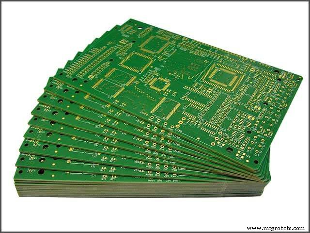
WellPCB を使用したプリント基板の製造
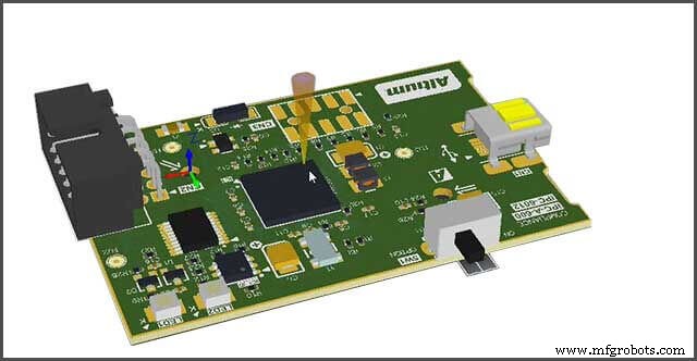
デバイスのプリント回路レイアウトの開発に成功したら、次はボードを作成する必要があります。製造を開始する前に、最終製品がどのように見えるかを確認することをお勧めします. Proteus や Altium などの一部のソフトウェアには 3D レイアウト ビューアがあり、ボードを 3D で表示して、ボードがどのように見えるかを感じることができます。
デザインを製造に送る前に、製造業者が使用するファイル形式を生成し、何を使用するかを決定する必要があります。 WellPCB は製造業のリーダーです。
プリント回路基板と、PCB 製造の仕事に最適です。
PCB 設計は、ほとんどの専門家が使用する、PCB 業界の標準であるガーバー ファイルに変換する必要があります。ガーバー ファイルには、PCB 製造で使用するために必要なすべての設計ファイルが含まれています。 WellPCB は 4 つのファイル形式(Gerber、pcb、pcbdoc、または cam ファイル形式)を受け入れます。
WellPCB は両面にシルクスクリーンを印刷し、追加料金はかかりません。印刷されたシルクスクリーン レイヤーに部品番号を含めると便利です。また、ボードハウスの仕様を知っておくとよいでしょう。 WellPCB のライン/トラック幅とスペースは最低 3mil です。デザインがそれを超えないようにしてください。ソフトウェア デザイン ルール チェックを使用して、ボードがメーカーの生産能力を超えていないことを確認してください。
シルクスクリーンの要件には、PCB 上の希望の色が記載されており、ほとんどが UV 硬化インクであり、RoHS に準拠しています。
1.白
2.イエロー
3. 黒
これらは最も広く使用されている色です。他のものも利用でき、色は処理時間とコストに追加される可能性があります。
WellPCB で PCB を注文するには、次の簡単な手順に従ってください:
4. WellPCB PCB オンライン見積もりセクションにアクセスします – https://www.wellpcb.com/pcb-quote
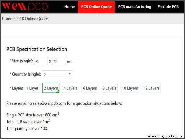
5. ボードの詳細を入力し、[カートに追加] をクリックします。カスタム PCB 回路基板のオンライン注文について知っておく必要があります。必要な PCB ボードについては、WellPCB までご連絡ください。最小数量は 5 ユニットですブレッドボード PCB
6. 新しいアカウントを登録します。
7. PCB ガーバーをアップロードします。 Brd ファイル。
8. 商品を注文して、配達されるのを待ちます。
WellPCB は、すべてのクライアント ファイルの完全な DRC チェックの実行にも役立ちます。これは、特に設計に問題やエラーがある場合に役立ちます。ボードの製造中に時間とお金を無駄にしないように、ユーザーに問題が通知されます。
座って、プリント回路基板が到着するのを待ちます。 PCB サービスの PCB 製造リード タイムは、少なくとも 24 時間、8 ~ 12 層 PCB の場合は最短で約 120 時間です。
次の章では、PCB の用語と WELLPCB の機能について説明します。
WellPCB PCB 機能と一般的な PCB 用語
WellPCB は、プリント回路基板の大手メーカーであり、PCB プロトタイプに付随するプリント回路基板アセンブリを提供しています。
This makes WellPCB your go-to manufacturer for your entire product development. Also, they provide Turnkey services for outsourcing the components for your electronic board. Breadboard PCB
WellPCB is focused on offering PCB prototypes services and not just large-scale manufacturing. Their PCB prototypes services go at a minimum of 5 units. Not only are they offering prototyping services but also packaged at some meager prices.
A promotional price of $3.99 for users looking for 1-2 layers, 10pcs PCB prototypes, and a board of less than 10cm*10cm.
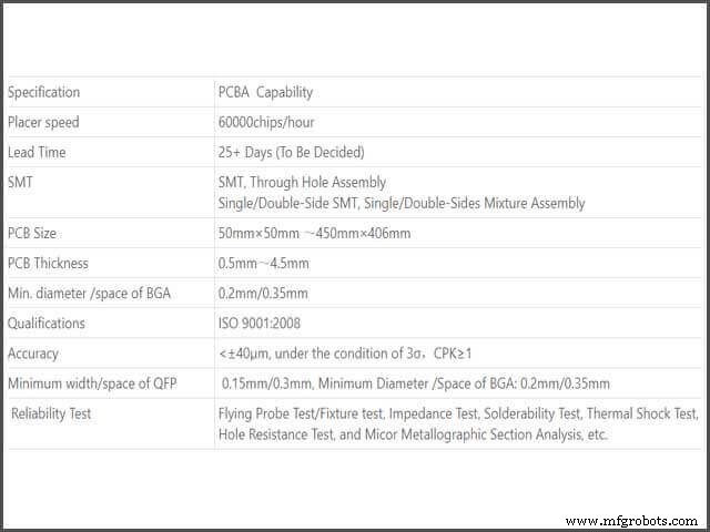
WELLPCB is capable of producing 100,000 square feet of 2-32-layer PCBs and delivering over 5000 varieties monthly.
With a quick turn to meet 24-hour delivery for double-sided PCBs, 48-hour for 4 to 8 layers, and 120-hour for ten layers or higher PCBs. Their standard lead time is about 5 – 6 days and an Expedited time of 24 – 48 hours.
4.1 The following are WellPCB PCB manufacturing capabilities
1. Support Material:FR4, High TG FR4, Halogen Free material, CEM-3, Rogers HF material.
2. Layer counts 1-32 layers.
3. Finished Copper Thickness:0.5-5 oz.
4. Finished Board Thickness:0.2-6.0mm.
5分。 Line/Track Width:4mil.
6. Min. Line/Track Space:4mil.
7. Min. Contour Tolerance:+/-0.1mm.
8. Min. Finished Diameter of PTH Hole:0.1mm.
9. Max. Board Thickness/Hole Ratio:12:1.
10. Min. Solder Mask Bridge:4mil (Min. SMT Pad Space 8mil).
11. Min. Legend(Silkscreen) Track Width:5mil.
12. Solder mask color:green, black, blue, white, yellow, matt, etc.
13. Solder mask hardness:6H.
14. Legend/Silkscreen Color:white, yellow, black, etc.
15. Surface Treatment:HAL, Lead-Free HAL, Immersion gold, OSP, Immersion Tin, Immersion silver, etc.
16. Other Technology:Gold finger, peelable mask, Non-across blinded vias, characteristic impedance control, Rigid-flex board, etc.
17. Reliability Test:flying probe test/fixture test, impedance test, solderability test, thermal shock test, hole resistance test.
18. Flammability:94V-0.
4.2 Breadboard PCB —Surface Finish
A PCB surface finish is a coating between a component and a bare board PCB. It is applied for two primary reasons:to ensure solderability and to protect the exposed copper circuitry.
Standard surface finishes preference – Non-RoHS or RoHS compliant.
1. HASL (Hot Air Solder Level) – Contains Lead non-RoHS, cheaper and quite popular.
2. ENIG (Electroless Nickel Immersion Gold) – Most popular finish and lead-free, but expensive
3. Immersion Silver – RoHS compliant will tarnish like any silver product
4. OSP – Organic Solderability Preservative
5. LF-HASL (Lead-Free Hot Air Solder Level)
6. Immersion Tin – Used the least of all finishes
4.3 Soldermask
Soldermask is the color to be used for the PCB prototypes finish. Any color can be used. However, sticking to standard colors is the best and more professional. The most popular are:
1. Green
2. Blue
3. Black
4. Red
5. White
6. Yellow
Mask can be in either Matte or Gloss in those above colors. Matte is less readily available due to Gloss is most widely used. Processing Matte for specific colors may add time due to equipment change and processing cleans up and application.
4.4 Breadboard PCB —Silkscreen
Silkscreen is the printing done on the PCB for identification. It is used on the component side to identify components, test points, PCBA part numbers, warning symbols, company logos, and manufacturer names. The following are some of the colors being used:
1. Black
2. White
3. Yellow
Those are the most widely used colors; others are available; however, colors can add to process time and cost like MASK. Ask if you have special requirements for your product.
In the next chapter, we will talk about how to move your PCBA mode.
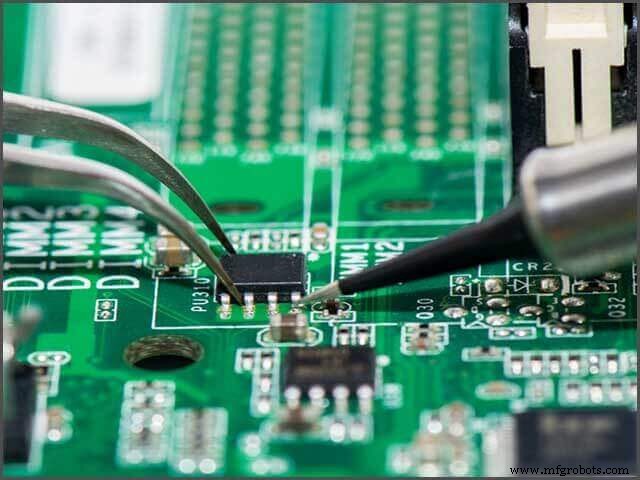
Breadboard PCB–Moving from PCB Prototypes to PCBA
So, what’s PCB Rapid Prototyping. PCB assembly. Directly speaking, PCB Rapid Prototyping. PCB assembly. Directly speaking, PCB Rapid Prototyping. 3D PCB Printing makes the PCB and does the Printed Circuit Board Assembly (PCBA, an abbreviation for printed circuit board assembly, which refers to the combination of PCB prototypes manufacture, components sourcing, and B3D PCB Printing makes the PCB and does the Printed Circuit Board Assembly PCBA is the PCB with components assembled).
So now you have your printed circuit board available and ready to populate the board with the needed components. You might be tempted to solder this manually yourself. This might be a good option, especially when the number of panels is less than five or, worst case, ten units; anything more than that might not be a good idea but going the route of PCB Rapid Prototyping. 3D PCB Printing not only makes the PCB but also does the Printed Circuit Board Assembly PCBA.
5.1 Breadboard PCB —Assembly Types of PCBA
The main assembly types of PCBA are shown below:
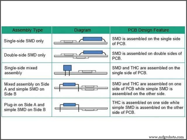
Those are the commonly used PCB Rapid Prototyping. 3D PCB Printing makes the PCB and does the Printed Circuit Board Assembly (PCBA assembly types. SMD means Surface Mount Devices, and THC implies Through Hole Components).
PCBA helps engineers, product developers, hobbyist and others to self-populate the board with needed components by a manufacturing firm.
It is usually faster and cheaper on bulk orders. Getting started with PCB Rapid Prototyping. 3D PCB Printing makes the PCB, and does the Printed Circuit Board Assembly (PCBA is also relatively simple as far you have the necessary resources).
Just like, WellPCB is capable of handling all your possible PCB prototypes works, they also offer an accompanying production film work that you require to manufacture PCBs. In the case of PCBA service to help one streamline the whole board development process. It does not cost much more to have the PCB populated unless you tack on additional steps in the process, such as burning a program to the MCU or running 100% test on the finished boards.
To get started with PCBA, you need to have all the required documents.
Aside from your PCB prototypes design file, you will need a design specification if there are special needs for your work, a bill of the material (BoM) list for the number of components on your board and also can be generated from the software being used, and part placements made from the software used.
When starting your PCB Assembly, one crucial take note is the sourcing of the components for the board.
The board owner can decide to source for the parts alone and send them to WELLPCB for assembly or let WellPCB handle the integral components sourcing, which I feel is better. Of course, partial supply can also be agreed upon.
Go to PCB Assembly on WellPCB here and fill the Request for Quotation (RFQ) form. Input as many details as possible and send it. WellPCB will get in touch if they need more information from you and continue the assembly process order.
The WellPCB Bill Of Materials (BOM) of a PCB gets fitted onto aboard. PCB Assembly process can take up to around 25 days for large volume manufacturing, which is an excellent time for large volume PCB assembly compared to other PCB Assembly manufacturers. This will make it easy for a pick and place machine to easily pick and place the components on the PCB Assembly capabilities:
More information about WellPCB SMT). This will make it easy for a pick and place machine to easily pick and place the components on the PCB Assembly capability can be found here.
At this point, all you have to do is to sit down and wait for your populated PCB to be available and sent to you. This concludes the end of this chapter, and the next chapter will discuss how to save money when doing PCB and PCBA.
Saving Money in PCB Prototypes and PCBA Manufacturing
Now congratulation, you have your fully developed hardware PCB prototypes or, better still, hardware board. For newbies, this will have been a good experience, and also a lot of money must have been sent which could have been avoided.
Some of the money spent could have been avoided due to unnecessary complexity and errors in the PCB and circuit design.
This chapter will show some of the handy tips and tricks that can help you save even millions when doing large volume manufacturing.
6.1 Breadboard PCB —Keep Your Board Size at a Minimum
Keeping your board size at a minimum is crucial in saving costs and making your final product as portable as possible. The bigger it gets, so do the prices. If the board becomes smaller, so does the cost.
Also, making your board too small might not save you cost since assembling and preparing your board might require specialized equipment.
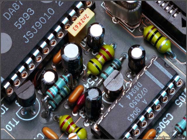
6.2 Using Surface Mount Components as Much as Possible
You might be tempted to use DIP (dual in-line) package, commonly known as Through-hole components, because it’s possible to easy to use but might not be the best cost-saving option.
1. Using surface mount components will reduce the number of holes that need to be drilled on your board typically used for through-hole parts.
2. Using surface mount components will also reduce the board size.
3. Using surface mount components will make the board assembly faster and lesser equipment used.
6.3 Set Your Design Up for Penalization
By going on board penalization, you can save yourself a ton of money. Getting all of your boards on one panel means that a rapid-fire pick and place machine can get all your parts placed in one go without requiring any additional setup time.
6.4 Silk Screening Help You Reduce Your PCB prototypes Costs?
Requesting silk screening on one side will cut your artwork costs in half. Sticking with standard colors and larger geometries will also prove beneficial. Understanding these constraints can help you to better PCB prototypes pricing and cost savings.
6.5 Breadboard PCB —Use the Right Via for the Job
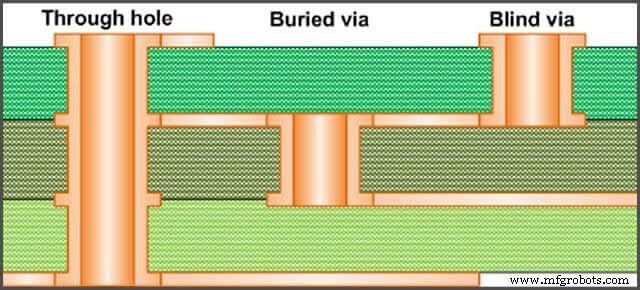
There are three types of vias – through-hole vias, blind vias, and buried vias. The last two are only going to be used for high-density and high-frequency PCBs. So, this one is simple, if your design doesn’t need these types of vias, leave them out to avoid any extra manufacturing costs.
This concludes the end of this chapter and the end of this guide. Using standard materials and several of these tips mentioned above can save you several thousand to millions of dollars when embarking on large volume manufacturing.
Breadboard PCB–Conclusion
When building and launching your products to market, some other things also need to be considered.
1. Certifications – Every wireless-based product needs to go through some certification process to be clear of any hazards or issues and be permitted to the market.
2. Enclosure – Depending on the type of product you are building, you might need some enclosure around your board to give it some artistic look or for some reason.
3. Quality Control – Quality control issues a formal inspection report for review and shipment approval. You should expect each shipment to be inspected and approved before being released. Such a protocol creates a closed-loop process that builds in continuous improvement for consecutive production runs.
This guide should give you enough head start in launching your following product. Taking an idea from concept to production is not for the faint of heart.
You have to withstand failures, criticism, mishaps, and managing the whole manufacture process can be very challenging. Still, a manufacturer like WellPCB is in the business to help you succeed. Breadboard PCB
産業技術