


高い紫外線検出効率のための4H-SiC分離吸収電荷と増倍アバランシェフォトダイオード構造の最適化戦略
要約
この作業では、構造最適化に関するパラメータ調査が、4H-SiCベースの分離吸収電荷および増倍(SACM)アバランシェ紫外線フォトダイオード(UV APD)に対して体系的に行われます。私たちの結果によると、絶縁破壊電圧は、増倍層の厚さと電荷制御層のドーピング濃度の影響を強く受ける可能性があります。 n型オーミック接触層、吸収層、電荷制御層の厚さは、光の侵入深さに大きく影響し、それに応じて光生成電子正孔対の数に影響を与えるため、前述の層の厚さはSACMAPDの応答性に大きな影響を与えます。 APDの応答性を高めるために、光吸収層と電荷制御層の界面でエネルギーバンドバリアの高さを低くする必要があります。これにより、増倍層へのキャリア輸送が促進されます。さらに、メサエッジでの電界を低減するために、角度が小さい正の斜角メサを調査します。したがって、それに応じて暗電流が抑制されます。
はじめに
ワイドバンドギャップ半導体材料として、炭化ケイ素(SiC)と窒化アルミニウムガリウム(AlGaN)は、高い臨界電界、優れた耐放射線効果、優れた熱伝導率などの優れた材料特性を示し、紫外線(UV)に適しています。検出[1,2,3]。 AlGaNベースの光検出器の3.4〜6.2 eVの調整可能なバンドギャップにより、365〜200nmの範囲の制御可能なカットオフ応答波長が可能になります。ただし、高品質のAlリッチAlGaN化合物の成長が難しいため、AlGaNベースの光検出器の暗電流はSiCベースの光検出器よりも高くなります[4]。したがって、SiCベースの光検出器は広範な研究の関心を集めています。最新の4H-SiCベースのソリッドステート紫外線検出器は、ショットキーバリアダイオード、金属-半導体-金属(MSM)フォトダイオード、p-i-nフォトダイオード、およびアバランシェフォトダイオード(APD)で構成されています[5、6、7、8、9]。 4H-SiC紫外線APDは、アバランシェゲインが高く、暗電流が小さく、ノイズが少ないため、火災警告、量子通信、ミサイル検出など、弱い紫外線信号の検出を必要とする多くの最先端分野で大きな応用が見込まれます。 10,11,12]。ただし、SiC材料は光吸収係数が低いため、増倍層が薄い一般的なフォトダイオード構造では、高い量子効率を実現することが困難です。分離された吸収電荷と増倍(SACM)構造APDが提案されるまで、問題は解決されません。一方では、UV光は吸収層によって効果的に吸収され、他方では、衝突電離プロセスによって高磁場増倍層で高い内部利得を得ることができます。増倍層での衝突電離プロセスは、電荷制御層によって終了させることができます[13、14]。 SACM構造の利点は、ノイズの低減にあります。これは、イオン化率の高い単一タイプの光生成キャリアのみを増倍層に注入できるためです[15、16]。弱い紫外線信号に対して高い検出率を得るには、アクティブな検出領域が大きいSACMAPDを製造する必要があります[17]。ただし、デバイスサイズが大きくなると、表面リーク電流とバルクリーク電流が大幅に増加します。したがって、これはSiCエピタキシャルウェーハの品質に厳しい要件を課すだけでなく、デバイス製造プロセスとデバイス設計への大きな課題を反映しています。過去数十年の間に、Cree CompanyはSiC膜のエピタキシャル成長技術を大幅に推進してきました。これにより、結晶品質の継続的な改善がさらに進んでいます。最近では、周ら。は、斜角の4H-SiC APDメサ[18]の非常に滑らかな側壁を作成するための可変温度フォトレジストリフロー技術を提案しました。これにより、10 6 を超える高い増倍ゲインが可能になります。 〜0.2 nA / cm 2 の低い暗電流 。それにもかかわらず、以前の研究は、材料品質の改善とSACM APDの製造技術の最適化に焦点を当てていましたが[19、20、21]、構造設計が光生成キャリア輸送と光電流検出に与える影響については、これまでほとんど議論されていませんでした。 。したがって、この手紙では、異なる構造設計の大面積4H-SiCベースのSACM紫外線APDのオプトエレクトロニクス性能を体系的に調査します。その間、洞察に満ちた物理的なイメージと議論も提供されます。この研究の結果は、研究者が4H-SiCAPDを低コストで最適化するのに役立つと信じています。
知られているように、大規模なキャリア増倍は、衝突電離が起こるときに生成されるが、それにもかかわらず、増倍層の厚さおよび電荷制御層のドーピング濃度によって強く影響される。非常に強い電界が増倍層で生成され、衝突電離が可能になります。電界は、その中のより大きなドーピング濃度のために、電荷制御層によって終端することができる。さらに、吸収層と電荷制御層の間のエネルギー帯域を変調することにより、スペクトル応答性を調整できることもわかりました。正の斜角メサを適切に採用することで、側壁表面の電界を大幅に低減できます。これは、暗電流とエッジの破壊を抑制するのに役立ちます。その後、詳細な分析と議論が行われます。
調査方法と物理モデル
図1aは、この作業で使用された、n + を持つ標準の4H-SiCSACMAPDの概略断面図を示しています。 -基板としてタイプ4H-SiC層。次に、アーキテクチャスタックは3μmの厚さのp + で構成されます。 -タイプレイヤー( N a =1×10 19 cm -3 )p型オーミック接触層として機能し、厚さ0.5μmのn - -型乗算層( N d =1×10 15 cm -3 )キャリア増倍の場合、厚さ0.2μmのn型電荷制御層( N d =5×10 18 cm -3 )衝突電離プロセスを終了するため、および厚さ0.5μmのn - タイプの吸収層( N d =1×10 15 cm -3 )入ってくる光子を吸収します。デバイス構造の上に、0.3μmの厚さのn + があります。 -タイプのオーミック接触層( N d =1×10 19 cm -3 )。正の斜角(θ =8°)は、エッジの破壊を抑制するためにメサ構造に対して作成されます[22、23]。 4H-SiC SACMAPDの直径は800μmです。カソードとアノードの両方の接点は、計算では理想的なオーミック接点と見なされます。図1cおよびdによると、前述の標準的な4H-SiC SACM APD構造の計算結果は、2.5 nA / cm 2 の暗電流を示しています。 、161.6 Vの絶縁破壊電圧、および280nmの波長で0.11A / Wのピーク応答性。標準の4H-SiCSACM APDについて計算された電流-電圧特性と応答性は、実験データと一致しています。これは、この作業で使用される衝突電離、4H-SiC材料吸収係数、ポアソン方程式、電流連続方程式、およびドリフト拡散方程式が妥当であることを完全に証明しています。ここでは、図1aの構造を調査ベンチマークとして採用し、調査対象の変数には、斜角のメサ角度、厚さ、各層のドーピング濃度が含まれています。
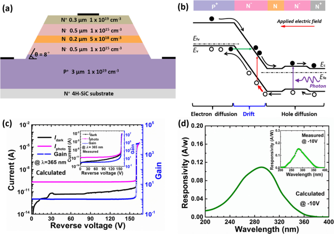
a 概略断面構造(縮尺どおりに描かれていない)、 b 標準の4H-SiCSACM APD、 c の逆バイアス下での概略エネルギーバンド図 計算された電流-電圧特性と増倍ゲイン、および d 標準の4H-SiCSACMAPDの逆電圧10Vで計算されたスペクトル応答特性。 c の挿入図 は、測定された電流-電圧特性と増倍ゲインを示しています。 d の挿入図 は、− 10 V
でバイアスされた標準4H-SiCSACMAPDの測定されたスペクトル応答特性を示しています。4H-SiC SACM APDの光電特性に対するさまざまな構造変数の影響をよりよく理解するために、図1bに逆バイアス下のエネルギーバンド図を示します。吸収層で光生成された電子正孔対は、電荷制御層を経由して増倍層に拡散します。光生成された電子正孔対が増倍領域に到達した後、それらは枯渇した電場によって分離されます。次に、ホールは増倍層で増倍プロセスを経験し、内部電流ゲインが発生します。その間、光生成された電子は陰極に戻り、衝突電離を経験することなく電流に変換されます。光電流に影響を与える重要な要因には、増倍層の電界プロファイル、電荷制御層、吸収層、およびエネルギー障壁がキャリア輸送を妨げる可能性のあるn型オーミック接触層のエネルギーバンドアライメントが含まれます。増倍層の電界プロファイルは、増倍層と電荷制御層の両方のドーピング濃度によって決定できることも注目に値します。一方、斜角のメサ角も実質的に電界分布に関連しています。また、各層の厚さにも注意を払い、高効率のキャリア拡散プロセスを確保します。したがって、デバイスのパフォーマンスを最適化するには、これらの主要な構造パラメータを体系的に調査することが重要です。
数値調査はAPSYSによって行われ、APSYSは、適切な境界条件と一貫して、電流連続方程式、ポアソン方程式、およびドリフト拡散方程式を解くことができます。衝突電離とツェナートンネリングプロセスの両方がドリフト拡散方程式に含まれています。キャリア輸送プロセスのキャリア-キャリア散乱も、低電界移動度モデルに含まれています。 Shockley-Read-Hall(SRH)の再結合寿命は1μsと想定されています[24]。具体的には、フィールド( E )電子の衝突電離係数の依存性(α n )と穴(β p )4H-SiCベースの層の場合、それぞれ次のようにChynowethの式(1)および(2)で表すことができます[25]:
$$ {\ alpha} _n =1.98 \ times {10} ^ 6 \ exp \ left [-{\ left(\ frac {9.46 \ times {10} ^ 6} {E} \ right)} ^ {1.42} \右] {\ mathrm {cm}} ^ {-1} $$(1)$$ {\ beta} _p =4.38 \ times {10} ^ 6 \ exp \ left [-{\ left(\ frac {1.14 \時間{10} ^ 7} {E} \ right)} ^ {1.06} \ right] {\ mathrm {cm}} ^ {-1} $$(2)4H-SiC材料の異なる波長(λ)に関する吸収係数(∂)は、次の式で計算されます。 (3)[26]:
$$ \ partial =-790.3 + 18.2 \ uplambda -0.17 {\ uplambda} ^ 2 + 8.57 \ times {10} ^ {-4} {\ uplambda} ^ 3-2.39 \ times {10} ^ {-6} { \ uplambda} ^ 4 + 3.53 \ times {10} ^ {-9} {\ uplambda} ^ 5-2.16 \ times {10} ^ {-12} {\ uplambda} ^ 6 $$(3)数値モデルで使用される他の材料パラメータは、他の場所で見つけることができます[27]。計算は有限要素法に基づいており、ユーザーは正確な計算を行うためにメッシュ分布を適切に調整する必要があります。
結果と考察
n型オーミック接触層の構造パラメータが光電性能に与える影響
n型オーミック接触層の厚さとドーピング濃度が光電性能に及ぼす影響を調べるために、参照デバイス、デバイスL1からL4、およびデバイスA1からA4をそれぞれ設計します。図1aに示すように、参照デバイスは基本的なSACMAPD構造であることに注意してください。他の提案されたAPDは、n型SiCオーミック接触層を除いて参照デバイスと同じです。詳細な構造情報は表1に示されています。
<図>まず、図2aのn型SiCオーミック接触層(デバイスL1〜L4)の絶縁破壊電圧を厚さで示します。図2aの挿入図は、暗電流、365 nmの照明下での光電流、およびデバイスL1のゲインを選択的に示しています。デバイスL1の場合、降伏電圧は〜161.6 Vであり、暗電流密度は〜2.5 nA / cm 2 のレベルのままです。 バイアスが161.6Vより低い場合。ブレークダウン電圧は10 -5 の電流で得られることに注意してください。 A.衝突電離プロセスが発生すると、暗電流が増加します。 365nmの照明がデバイスを照らすと、線形領域で光電流レベルが高くなります。これは、増倍ゲインが10 3 を超える可能性があることを示しています。 逆電圧161.6VのデバイスL1の場合。調査した5つのAPDのアバランシェ降伏電圧を図2aにまとめています。図2aから、n型オーミック接触層の厚さが絶縁破壊電圧に与える影響はごくわずかであることがわかります。観測の基礎となるメカニズムを明らかにするために、参照デバイスとデバイスL1〜L4の垂直電界分布を計算して図2bに示します。これは、電荷制御層が空乏領域と電界の境界を制限していることを示しています。乗算層。したがって、n型オーミック接触層は増倍層の電界プロファイルに影響を与えないと推測できます。これは図2bで証明されています。図2bの観察結果は、参照デバイスとデバイスL1〜L4の図2aと同じ絶縁破壊電圧をよく解釈しています。次に、図2cに5つのデバイスの光生成電流を示します。解像度を上げるために、図2cの挿入図に示されている100Vのバイアスで光生成電流を収集します。 n型オーミックコンタクト層の厚みが増すにつれて、光生成電流が減少することがわかります。厚すぎるn型オーミック接触層は、光生成されたキャリアに非放射再結合を引き起こし、それに応じて拡散電流を減少させます。光生成電流を使用すると、図2dの逆電圧100 Vで、参照デバイスとデバイスL1〜L4のスペクトル応答性を取得できます。調査した5つのデバイスのピーク応答波長は280nmを中心としています。応答性は、n型接触層の厚さが増すにつれて低下します。これは、図2cの挿入図と一致しています。したがって、ここでは、n型4H-SiCオーミック接触層の厚さを適切に薄くして、非放射再結合の増加と拡散電流の減少を回避する必要があることを要約します。
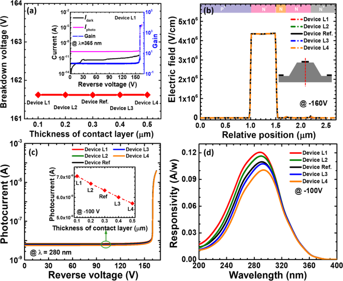
a 絶縁破壊電圧、 b − 160 V、 c でバイアスされたSACMAPDの垂直電界分布 280 nmの照明下での光電流-電圧特性、および d 参照デバイスおよびn型オーミック接触層の厚さがそれぞれ異なるデバイスL1〜L4について、-100VでバイアスされたSACMAPDのスペクトル応答特性。 a の挿入図 は、デバイスL1の計算された電流-電圧特性と乗算ゲインを示しています。 c の挿入図 は、リファレンスデバイスとデバイスL1〜L4が− 100 V
でバイアスされた場合の光電流を示しています。次に、図3aの参照デバイスとデバイスA1〜A4を分析することにより、n型オーミック接触層のドーピング濃度の関数としての絶縁破壊電圧を調査します。図3aの挿入図は、暗電流、光生成電流、およびデバイスA1に適用されたバイアスに関するゲインを示しています。絶縁破壊電圧は、電流が10 -5 に達したときに定義されます。 A.図3aによると、絶縁破壊電圧は、n型4H-SiCオーミック接触層のドーピング濃度にほとんど依存しません。先に示したように、電荷制御層は、空乏領域と電場を増倍層に効果的に閉じ込めることができます。したがって、n型オーミック接触層のドーピング濃度の変動は、デバイス内の電界分布に影響を与えません[図3bを参照]。次に、参照デバイスとデバイスA1〜A4に適用されたバイアスの観点から、光生成電流を計算して図3cに示します。図3cから、n型オーミック接触層のドーピング濃度がバイアスされた光電流に与える影響はごくわずかであることがわかります。調査した5つのデバイスのさまざまな波長でのスペクトル応答性を図3dに示します。データは100Vの逆電圧で計算されます。最大応答性が〜0.11 A / Wの波長は280nmです。図3cと一致しているため、応答性はn型オーミック接触層のドーピング濃度にあまり依存しません。したがって、応答性は、4H-SiC SACMAPDのn型オーミック接触層のドーピング濃度よりも厚さの影響を強く受けると結論付けます。また、応答性を高めるために、キャリア拡散長を長くすることをお勧めします。
a 絶縁破壊電圧、 b − 160 V、 c でバイアスされたSACMAPDの垂直電界分布 280 nmの照明下での光電流-電圧特性、および d 参照デバイスおよびn型オーミック接触層のドーピング濃度が異なるデバイスA1〜A4について、それぞれ-100VでバイアスされたSACMAPDのスペクトル応答特性。 a の挿入図 は、デバイスA1の計算された電流-電圧特性と乗算ゲインを示しています。 c の挿入図 は、リファレンスデバイスとデバイスA1〜A4が− 100 V
でバイアスされた場合の光電流を示しています。吸収層の構造パラメータが光電性能に与える影響
このセクションでは、吸収層の厚さとドーピング濃度が4H-SiCベースのSACMAPDの光電性能に与える影響を調べます。 SACM APDの吸収層の詳細な構造情報を要約し、表2に示します。デバイスM1〜M4およびデバイスB1〜B4は、吸収層を除いて参照デバイスと構造的に同じです。デバイスM1からM4の厚さは異なりますが、デバイスB1からB4は、吸収層に対してさまざまなドーピング濃度を持っています。
<図>図4aは、参照デバイスとデバイスM1〜M4を使用して、吸収層のさまざまな厚さに関する絶縁破壊電圧を示しています。デモンストレーションの目的で、図4aの挿入図に、デバイスM1に適用されたバイアスの関数として、暗電流、光生成電流、およびゲインを計算して示します。ブレークダウン電圧は、電流が10 -5 のときに収集されます。 A.絶縁破壊電圧は、吸収層の厚さにほとんど依存しないことがわかります。絶縁破壊電圧は、軽くドープされた増倍層の電界強度の影響を強く受けることが知られているため、図4bは、逆バイアス-160Vでの5つの調査対象デバイスの垂直電界分布を示しています。参照デバイスとデバイスM1〜M4の電界分布はまったく同じであり、図4aの結論を裏付けています。続いて、光生成電流と応答性を図1と図2に示します。それぞれ4cとd。光生成電流[図4cの挿入図を参照]と応答性の両方が、吸収層の厚さが増すにつれて減少する傾向を示しています。根本的なメカニズムにさらに取り組むために、調査した5つのデバイスの逆バイアスが100 Vの場合の、図4eの増倍層内のキャリア分布も計算して示します。電子と正孔の両方の濃度レベルは、吸収層の厚さが増すにつれて減少することがわかります。これは、吸収層が厚くなると非放射再結合が強化されるためです。非放射再結合はキャリアを消費するため、拡散電流と応答性が抑制されます。ここでは、非放射再結合によるキャリア消費を回避するために、吸収層が厚すぎて、検出率の高い4H-SiC SACMAPDを取得できないようにすることをお勧めします。
a 絶縁破壊電圧、 b − 160 V、 c でバイアスされたSACMAPDの垂直電界分布 280 nmの照明下での光電流-電圧特性、 d スペクトル応答特性、および e 参照デバイスおよび吸収層の厚さが異なるデバイスM1〜M4について、それぞれ-100VでバイアスされたSACMAPDの増倍層のキャリア濃度プロファイル。 a の挿入図 は、デバイスM1の計算された電流-電圧特性と乗算ゲインを示しています。 c の挿入図 は、リファレンスデバイスとデバイスM1〜M4が− 100 V
でバイアスされた場合の光電流を示しています。吸収層の厚さに加えて、吸収層のドーピング濃度もデバイスの性能に大きな影響を与えます。次に、参照デバイスとデバイスB1〜B4の絶縁破壊電圧を計算して図5aに示します。絶縁破壊電圧は、電流が10 -5 のときに定義されます。 図5aの挿入図に示されているA。図5aから、吸収層のドーピング濃度は絶縁破壊電圧に大きな影響を与えないことがわかります。図5bの垂直方向の一次元電界分布によってさらに証明できるため、吸収層のドーピング濃度によって増倍層の電界プロファイルが大幅に変化することはありません。また、図5cに、調査対象のデバイスの波長280 nmでの光生成電流を示します。これは、吸収層のドーピング濃度が増加したときに光生成電流が改善されたことを示しています。図5cとよく一致して、図5dの波長依存の応答性も、吸収層のドーピング濃度が増加するにつれて優先されます(デバイスB4など)。
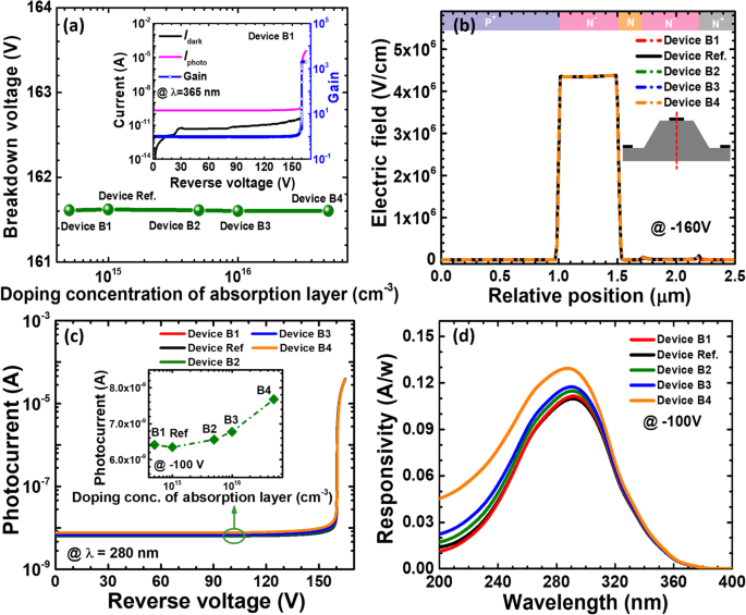
a 絶縁破壊電圧、 b − 160 V、 c でバイアスされたSACMAPDの垂直電界分布 280 nmの照明下での光電流-電圧特性、および d 参照デバイスと、吸収層のドーピング濃度が異なるデバイスB1〜B4について、それぞれ-100VでバイアスされたSACMAPDのスペクトル応答特性。 a の挿入図 は、デバイスB1の計算された電流-電圧特性と乗算ゲインを示しています。 c の挿入図 は、リファレンスデバイスとデバイスB1〜B4が− 100 V
でバイアスされた場合の光電流を示しています。デバイスB4の応答性の向上の詳細な起源を示すために、デバイスB1およびB4の電荷制御層、吸収層、およびn型オーミック接触層のエネルギーバンドプロファイルを図1および2に示します。それぞれ6aとb。ここで、電荷制御層とn型オーミック接触層のドーピング濃度は5×10 18 であることに言及する価値があります。 cm -3 および1×10 19 cm -3 、 それぞれ。したがって、吸収層のドーピング濃度を低くすると、ビルトイン電界が生成され、電荷制御層/吸収層/ n型オーミック接触層の界面にエネルギー障壁が生じる可能性があります[28]。エネルギー障壁は、光生成されたキャリアの増倍層への拡散を遅らせることができます。障壁を減らすことができる非常に便利な方法は、吸収層のドーピング濃度を上げることです。その結果、実効価電子帯障壁値ψ v 電荷制御層の場合、デバイスB1とB4の場合はそれぞれ513meVと480meVです。吸収層のドーピング濃度が高くなると、光生成された正孔の輸送が促進されることがわかります[図6cを参照]。衝突電離は、光生成された正孔を増倍領域に注入できるようになると強くなり、それに応じて光生成電流と応答性が向上します。
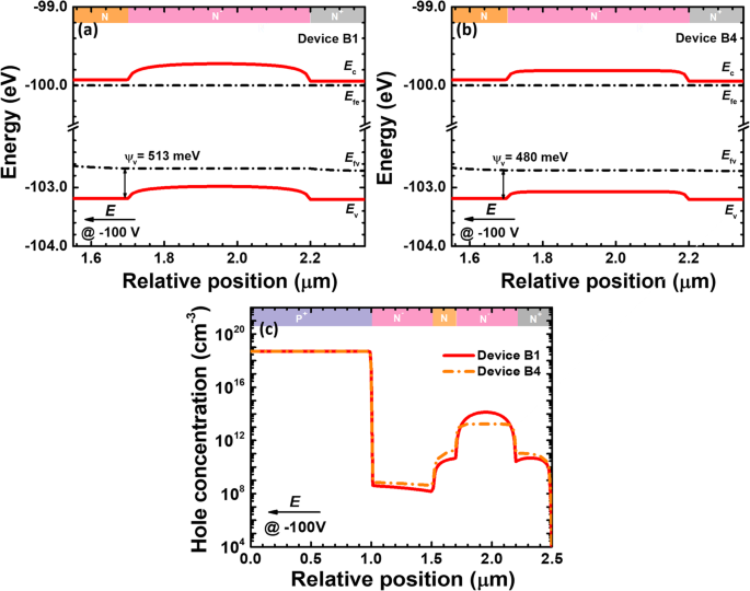
a の電荷制御層、吸収層、n型オーミック接触層のエネルギーバンド図 デバイスB1および b デバイスB4、 c デバイスB1およびB4の280nm照明下での正孔濃度プロファイル。データは100Vの逆電圧で計算されます
電荷制御層の構造パラメータが光電性能に与える影響
電荷制御層の厚さとドーピング濃度が光電性能に与える影響を調べるために、表3に示すように、電荷制御層に異なるアーキテクチャ情報を設定しました。デバイスN1〜N4およびデバイスC1〜C4は、参照デバイスとのみ異なります。電荷制御層で。デバイスN1からN4およびC1からC4には、異なるドーピング濃度と層の厚さが採用されています。
<図>前述のように、衝突電離とアバランシェ降伏を可能にする電界は、主に増倍層に閉じ込められます。図7aの電荷制御層の厚さの関数としての絶縁破壊電圧は、電荷制御層の厚さがキャリア増倍プロセスにごくわずかな影響しか及ぼさないことを示しています。これは、図7bを示すことによってさらに証明されます。図7cは、参照デバイスとデバイスN1〜N4に適用されたバイアスの観点から光生成電流を示しています。電荷制御層の厚さが増加すると、光生成電流は低くなります。これは、電荷制御層の厚さが増加するにつれて応答性が小さくなることも意味します。また、キャリアを消費し、拡散電流を抑制する強化された非放射再結合に起因します。
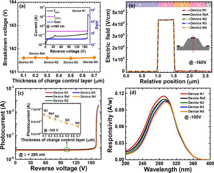
a 絶縁破壊電圧、 b − 160 V、 c でバイアスされたSACMAPDの垂直電界分布 280 nmの照明下での光電流-電圧特性、および d 参照デバイスと、電荷制御層の厚さが異なるデバイスN1〜N4について、それぞれ-100VでバイアスされたSACMAPDのスペクトル応答特性。 a の挿入図 は、デバイスN1の計算された電流-電圧特性と乗算ゲインを示しています。 c の挿入図 は、リファレンスデバイスとデバイスN1〜N4が− 100 V
でバイアスされた場合の光電流を示しています。電荷制御層の役割は、強電界とキャリア増倍プロセスを増倍層内に閉じ込めることです。しかしながら、電荷制御層におけるドーピング濃度が減少する限り、空乏領域幅はさらに拡大され得る。その場合、電界プロファイルは、絶縁破壊電圧、光生成電流、ゲイン、および応答性に実質的に影響を与える可能性があります。したがって、表3のデバイスC1〜C4を設計します。図8aによると、ドーピング濃度が低下すると、ブレークダウン電圧は最初は同じままで、電荷制御層のドーピング濃度が2未満になるとブレークダウン電圧が上昇します。 ×10 18 cm -3 。図8aの挿入図は、デバイスC1の絶縁破壊電圧が〜315 Vであるのに対し、暗電流も3.5×10 -11 に上昇することを示しています。 デバイスN1との比較。図8aの観測の起源を明らかにするために、図8bの垂直電界分布を計算します。これは、電界が主に参照デバイスとデバイスC3およびC4の増倍層に集中していることを示しています。ただし、電荷制御層のドーピング濃度が2×10 18 未満の場合、電界と空乏領域が電荷制御層に浸透します。 cm -3 。デバイスC1およびC2の空乏領域の拡大は、電界強度を低減するのに役立ち、したがって、デバイスC1およびC2のブレークダウン電圧はそれに応じて増加します。空乏領域の幅が大きくなると、より多くの空間電荷生成電流が発生し、その結果、暗電流が増加します。つまり、3.5×10 − 11 になります。 Aおよび5×10 − 11 それぞれデバイスC1とC2のA。次に、波長280nmでの光生成電流を図8cに示します。 The 100V-biased spectral responsivity curves at different wavelengths for the five investigated devices are illustrated in Fig. 8d. Excellent agreement is obtained between Figs. 8c and d, such that the increased photo-generated current gives rise to the enhanced responsivity, i.e., devices C1 and C2. Other devices show similar photo-current level and the responsivity.

a Breakdown voltage, b vertical electric field distribution of the SACM APDs biased at − 160 V, c photocurrent biased at − 100 V, and d spectral response characteristics of the SACM APDs biased at − 100 V for reference device and devices C1 to C4 with different doping concentration of charge control layer, respectively. Inset figure in a shows the calculated current-voltage characteristics and the multiplication gain for device C1. Inset figure in c shows photocurrent-voltage characteristics for reference device and devices C1 to C4
As has been interpreted previously, the energy band barrier height at the interface of multiplication layer/charge control layer can soundly affect the carrier diffusion. Due to the expansion of the depletion region for devices C1 and C2, the electric field in the depletion region will annihilate the energy barrier at the interface of multiplication layer/charge control layer [e.g., the inset for device C1 in Fig. 9a]. Meanwhile, we observe the valence band barrier at the interface of multiplication layer/charge control layer for device C4 according to the inset for Fig. 9b. The energy barrier will correspondingly retard the hole diffusion into the multiplication layer from the charge control layer. We also selectively compute and show the hole concentration profiles for device C1 and C4 in Fig. 9c. Because the interface of multiplication layer/charge control layer for device C1 no longer hinders the injection of photo-generated holes into the multiplication layer, more holes are limited in the charge control layer and the absorption layer for device C4. As a result, the hole concentration in the multiplication layer for device C1 is higher than that for device C4. Thus, the enhanced photo-generated current and the responsivity for device C1 are obtained when compared with device C4.

Energy band diagrams for a device C1 and b device C4, c hole concentration profiles for device C1 and C4. Data are calculated at the reverse voltage of 100 V. Insets for a および b show the local energy band diagrams for multiplication layer/charge control layer for devices C1 and C4, respectively
Impact of the Structural Parameters for the Multiplication Layer on the Photoelectric Performance
The impact ionization and the carrier multiplication process take place in the multiplication layer, making the design for the multiplication layer essentially vital for 4H-SiC SACM APDs. Therefore, we look into the impact of the thickness and doping concentration for the multiplication layer on the photoelectric performance for SACM APDs. The detailed structural information of the multiplication layer for different SACM APDs are summarized and presented in Table 4. The only difference for the devices in Table 4 lies on the multiplication layer.
<図>As Fig. 10a presents, the breakdown voltage is enhanced from 110 to 210 V when the multiplication layer thickness is increased from 0.3 to 0.7 μm. For the purpose of demonstration, the inset of Fig. 10a demonstrates the current in terms of the voltage for reference device and devices P1 to P4. This indicates that a thick multiplication layer helps to reduce the electric field intensity [see Fig. 10b] and increase the breakdown voltage. We then show the photo-generated current for the five devices in Fig. 10c. The photo-generated current increases slightly with increasing the thickness of the multiplication layer for devices P2 to P4, except that device P1 has the highest photocurrent. The spectral responsivity characteristics for the five investigated devices at the reverse voltage of 100 V are provided in Fig. 10d. The peak responsivity for reference device and devices P2 to P4 improves slightly as the thickness of the multiplication layer increases, and this is because the number of carriers generated by impact ionization increases when the depletion region width increases. Note that device P1 with the thinnest multiplication layer owns the highest peak responsivity at the wavelength of 280 nm. This is because the − 100 V applied voltage is close to Geiger mode for device P1, and the avalanche gain is more likely to occur than that for other devices.

a Breakdown voltage, b vertical electric field distribution of the SACM APDs biased at − 160 V, c photocurrent biased at − 100 V, and d spectral response characteristics of the SACM APDs biased at − 100 V for reference device and devices P1 to P4 with different thicknesses of multiplication layer, respectively. Inset figure in a shows the calculated current-voltage characteristics for reference device and devices P1 to P4. Inset figure in c shows photocurrent-voltage characteristics under 280 nm illumination for reference device and devices P1 to P4
Then, we show the breakdown voltage in terms of the multiplication layer doping concentration for reference device and devices D1 to D4 in Fig. 11a. It seems that when the doping concentration for the multiplication layer is lower than 10 16 cm -3 , the breakdown voltage is less affected. We believe the breakdown voltage can be significantly decreased if the doping concentration in the multiplication layer exceeds 10 18 cm -3 。 The dark current as a function of the applied bias for the five APDs are shown in the inset of Fig. 11a. The dark current increases with increasing doping concentration of the multiplication layer due to the enhanced space charge generation in the depletion region. Therefore, for the purpose of significantly decreasing the dark current and promoting the carrier multiplication process, we rarely have the multiplication layer heavily doped. Then, we calculate the vertical one-dimensional electric field profiles for the five studied devices, which are demonstrated in Fig. 11b. We can see that the electric field profiles of the five devices are mainly confined in the multiplication layer. In addition, Figs. 11c and d demonstrate the photo-generated current and the wavelength-dependent responsivity for the five devices. We can see that the photo-generated current for reference device and devices D1 and D2 are almost the same under the 280 nm illumination, while that the photon-generated current for the devices D3 and D4 is slightly increased. Therefore, the responsivity at the wavelength of 280 nm in Fig. 11d for devices D3 and D4 is slightly higher than the others.

a Breakdown voltage, b vertical electric field distribution of the SACM APDs biased at − 160 V, c photocurrent-voltage characteristics under 280 nm illumination, and d spectral response characteristics of the SACM APDs biased at − 100 V for reference device and devices D1 to D4 with different doping concentration of multiplication layer, respectively. Inset figure in a shows the calculated current-voltage characteristics for reference device and devices D1 to D4. Inset figure in c shows photocurrent for reference device and devices D1 to D4 biased at − 100 V
Impact of the Beveled Mesa Angle on the Photoelectric Performance
In order to eliminate premature breakdown and suppress leakage current that are caused by the junction termination, positive beveled mesas with a small inclination angle are usually adopted when fabricating 4H-SiC APDs [13,14,15,16, 18]. However, the angles of the positive beveled mesa adopted in previous reports are various. Thus, to get systematic insight into the influence of different mesa inclination angles on the electric field profiles for 4H-SiC SACM APDs, we design the devices that are shown in Table 5.
<図>We firstly calculate and show the dark current-voltage characteristics for the six investigated devices with the various bevel angles in Fig. 12a. We can see that the dark current increases as the positive beveled angle becomes large [see Fig. 12a]. The breakdown voltages for the investigated devices are ~ 161.6 V except that device E5 is slightly less than 161.6 V. The premature breakdown is observed as the beveled mesa angle increase in the dark condition. Meanwhile, we calculate and show photo-generated current in terms of the applied bias for reference device and devices E1 to E5 in Fig. 12b. We also see that the photo-generated current also increases as the positive bevel increases according to the inset for Fig. 12b. The premature breakdown is also observed as the beveled mesa angle increase in Fig. 12b. Therefore, the responsivity of solar-blind waveband at − 100 V slightly enhances as the positive bevel angle increases according to Fig. 12c.

a Numerically calculated dark current-voltage characteristics, b photocurrent-voltage characteristics under 280 nm illumination, and c spectral response characteristics of the SACM APDs biased at − 100 V for reference device and devices E1 to E5, respectively
To reveal the origin for the observations in Figs. 12a and b, we calculate the lateral electric field distribution in the multiplication layer at the reverse bias of − 100 V in Fig. 13a, which demonstrates that, when the beveled mesas are utilized, the electric field decreases from the mesa center to the mesa edge. Moreover, the edge electric field intensity drops as the angle further decreases for the investigated devices. As has been mentioned, the junction termination will cause a large number of surface imperfections, which may cause the premature breakdown and the strongly leakage current, and the adopting of the beveled mesa shifts the premature breakdown from the mesa surface to the bulk [29]. Moreover, to get a full picture for the electric field profiles, the two-dimensional electric field distributions at the reverse bias of − 100 V for reference device and devices E1 to E5 are presented in Figs. 13b-g. We can see that the area of the high electric field in the entire multiplication layer gets narrowed, and this simultaneously causes the carriers that regenerated by impact ionization to decrease. As can be seen from Table 6, as the beveled mesa angle decreases, the surface electric field at the relative position of 700 μm decreases from 2.03 × 10 6 V/cm to 2.90 × 10 5 V/cm. As a result, the surface leakage and bulk leakage can be further suppressed as the beveled mesa angle get further decreased as shown in Fig. 12a. Although a small beveled mesa angle is preferred, this sacrifices the active detection area for APDs, and therefore, the responsivity is the lowest for device E1 according to Fig. 12c. Thus, one shall properly optimize beveled mesa angles depending on the crystalline quality for the 4H-SiC epitaxial layers and the surface conditions after junction termination. The suggested beveled angle in this works is in the range of 10–20°.

a Lateral electric field distribution of the multiplication layer at − 100 V, and numerically calculated two-dimensional electric field distribution at − 100 V for b device E1, c reference device, d device E2, e device E3, f device E4 and g device E5
結論
To summarize, we have numerically investigated and demonstrated the impact of the thickness and doping concentration of each layer on photoelectric performance for 4H-SiC SACM APDs. The obtained conclusions are as follows:(1) for n-type ohmic contact layer with a properly high doping concentration (N d ≈ 1 × 10 19 cm -3 ) to enable ohmic contact, the thickness and doping concentration hardly affect the breakdown voltage. Nevertheless, the responsivity decreases as the thickness of the n-type ohmic contact layer increases. The thickness shall be controlled to about 0.2 μm; (2) the doping concentration for the absorption layer is vitally important, which can modulate the photo-generated carrier transport and affect the responsivity. The doping concentration is generally controlled at the intrinsic concentration (N d ≈ 1 × 10 15 cm -3 ); (3) the doping concentration for the charge control layer regulates the electric field distribution and affects the depletion region width for 4H-SiC SACM APDs. The depletion region width increases as the doping concentration of the charge control layer decreases. According to our results, when the doping concentration is about 1 × 10 18 cm -3 , the depletion region can be completely terminated by the charge control layer; (4) the breakdown voltage can be strongly affected by the thickness of multiplication layer which is the main support region of the electric field. The dark current is sensitive to the doping concentration of multiplication layer, and a low doping concentration for the multiplication layer is required, since the doping concentration therein influences the space charge generation current. Thus, the suggested doping concentration in this works is intrinsic concentration (N d ≈ 1 × 10 15 cm -3 ); (5) we also point out the advantage of beveled mesa for 4H-SiC SACM APDs, and the optimized beveled mesa angles shall be a compromise among the active detection area, the surface conditions for the mesa, and the crystalline quality for 4H-SiC epitaxial films. This work indicates that the optimum beveled mesa angle is in the range of 10–20°. We strongly believe that this work provides the physical insight for the device physics and hence the findings in this work are very important for 4H-SiC-based SACM APDs.
データと資料の可用性
現在の作業のデータと分析は、合理的な要求に応じて対応する著者から入手できます。
略語
- AlGaN:
-
Aluminum gallium nitride
- APSYS:
-
Advanced Physical Models of Semiconductor Devices
- MSM:
-
金属-半導体-金属
- SACM:
-
Separated absorption charge and multiplication
- SiC:
-
炭化ケイ素
- SRH:
-
Shockley-Read-Hall
- UV APD:
-
Avalanche ultraviolet photodiode
ナノマテリアル
- 壊れたメンテナンス戦略の修正:PM最適化とFMEA
- 卵巣癌細胞の高感度かつ迅速な検出のための柔軟なグラフェンベースのバイオセンサーのデモンストレーション
- マイクロLEDおよびVCSEL用の高度な原子層堆積技術
- スリーステートエレクトロクロミックデバイスのディップコーティングプロセスエンジニアリングと性能最適化
- 高効率偏光ビームスプリッターと光渦発生器のための高次誘電体メタ表面
- スパイラル型アンテナによるマイクロブリッジ構造のTHzマイクロボロメータの周波数変調と吸収改善
- 高いMgドーピング効率のために特別に設計された超格子p型電子ブロッキング層を備えたほぼ効率の低いAlGaNベースの紫外線発光ダイオード
- ニオブ酸スズ光触媒の操舵電荷速度論:相構造と電子構造の重要な役割
- AlGaNベースの深紫外線発光ダイオード用のp-AlGaN / n-AlGaN / p-AlGaN電流拡散層について
- PCB材料と高電圧用の設計
- 生産と効率のための VMC 機械