


低電流密度での量子効率を改善するためのInGaNマイクロLED構造の設計
要約
ここでは、低電流密度での窒化物マイクロ発光ダイオード(マイクロLED)の動作動作と物理的メカニズムに関する包括的な数値研究を報告します。偏光効果の分析は、マイクロLEDが低電流密度でより厳しい量子閉じ込めシュタルク効果を被ることを示しています。これは、効率の向上と安定したフルカラー発光の実現に課題をもたらします。キャリアの輸送とマッチングを分析して、最適な動作条件を決定し、低電流密度でのマイクロLEDの構造設計を最適化します。活性領域の量子井戸数が少ないと、キャリアマッチングと放射再結合率が向上し、量子効率と出力パワーが高くなることが示されています。マイクロLED用の電子ブロッキング層(EBL)の有効性について説明します。 EBLを除去することにより、電子の閉じ込めと正孔の注入が同時に改善されることがわかります。したがって、マイクロLEDの発光は、低電流密度で大幅に向上します。 AugerとShockley–Read–Hallに関する再結合プロセスが調査され、欠陥に対する感度が低電流密度のマイクロLEDで強調されています。
あらすじ :低電流密度で動作するInGaNマイクロLEDの分極誘起QCSE、キャリア輸送とマッチング、および再結合プロセスを数値的に調査します。これらのデバイスの動作とメカニズムの理解に基づいて、高濃度にドープされた、またはEBLなしの2つのQWと、効率的なマイクロLED発光ディスプレイ用の高正孔濃度のp-GaNを含む特別に設計されたエピタキシャル構造が提案されます。マイクロLEDの場合、欠陥密度に対する感度も強調されています。
はじめに
III族窒化物ベースの可視発光ダイオード(LED)には、信号、光通信、情報ストレージ、バックライト、ディスプレイ、一般照明(またはソリッドステート照明)など、幅広い用途があります[1、2]。 2000年にJiangと彼の同僚によって直径12μmのInGaNマイクロディスクLEDの最初のデモンストレーションが行われて以来[3、4]、マイクロLEDは高解像度ディスプレイの分野で学術的および産業的関心を拡大してきました。 、可視光通信、生物医学、およびセンシング[5,6,7,8]。マイクロLEDは、液晶ディスプレイ(LCD)や有機発光ダイオード(OLED)と比較して、サイズが小さく、解像度が高く、発光効率が高く、輝度が高く、色飽和度が高く、動作寿命が長く、応答速度が速いという利点があります。堅牢性と堅牢性により、次世代ディスプレイ技術の最も有望な候補となっています[9、10]。マイクロLEDディスプレイのアプリケーションシナリオには、ハイエンドテレビ(TV)、ラップトップ、ハンドヘルドおよびモバイル端末デバイス、仮想現実(VR)、拡張現実(AR)、透明ディスプレイなどが含まれます。 Yoleの見積もりによると、マイクロLEDディスプレイの市場は2025年までに3億3000万台に達するでしょう[11]。
III族窒化物LEDの従来の用途、特にソリッドステート照明では、光出力を可能な限り高くする必要があります[12]。過去30年間で、高出力アプリケーション、エピタキシャル構造の設計と最適化、デバイスの動作動作と物理的メカニズムの研究、製造技術の改善など、窒化物LEDの最新の研究に動機付けられました。主に大型チップ、高動作電流密度、高入出力電力に焦点を当てています[12、13]。何よりも、窒化物LEDの活性領域は、初期の最も単純なヘテロ構造と単一量子井戸(QW)から、5周期のQWを持つ今日の多重量子井戸(MQW)に進化し、QW数は数回で8または10に達することさえあります。商用化されたハイパワーデバイス[14、15、16、17]。 EBLは、高い注入電流密度での電子の漏れをブロックするために提案されましたが、それでも特定のレベルで正孔注入を妨げる可能性があります[18、19]。従来の高出力LEDの場合、最も重要な問題は、電流密度の増加に伴う外部量子効率(EQE)の低下です。これは、効率低下として知られています。この振る舞いの本質的なメカニズムは、高い注入キャリア密度での間接的なオージェ再結合に関連しています[20]。製造に関しては、窒化物LEDの出力レベルを拡張するために薄膜フリップチップと垂直注入ジオメトリが開発されています[21、22]。
従来の大型高出力窒化物LEDにはかなりの進歩があり、学んだ教訓のいくつかはマイクロLEDの研究に活用できます。ただし、マイクロLEDは、高出力のLEDとはまだ大きく異なります。マイクロLEDのさまざまな動作動作、メカニズム、および条件は、さまざまな課題と研究経路をもたらす可能性があります[23、24]。従来のLEDの場合、ピークEQEは高電流密度にあり、動作電流密度は高く、ピーク効率を超えています(> 30 A cm -2 )。ただし、マイクロLED発光ディスプレイの場合、動作電流密度ははるかに低く、多くの場合0.02〜2 A cm -2 の範囲である必要があります。 [24]。この低電流密度では、従来の窒化物LEDのEQEは非常に低く、実際のマイクロLEDディスプレイアプリケーションには不十分です。 Vピットの利点を利用して転位をスクリーニングし、正孔注入を強化することにより、Zhangと彼の共同研究は、0.8 A / cm 2 で最大24.0%のピーク効率を持つ効率的なInGaNベースのLEDを作成しました。 。ただし、Zhangらによって報告されたLEDチップ。まだ従来のサイズ(1mm×1mm)に制限されており、マイクロLEDよりもはるかに大きい[25]。さらに、多くの研究で、マイクロLEDの内部量子効率(IQE)とEQEは、チップサイズが小さくなると低下することが報告されています[26、27、28]。このサイズに依存する劣化は、主に、プラズマ支援ドライエッチングによって引き起こされる表面の再結合と側壁の損傷に起因します。これらの側壁効果は、Shockley–Read–Hall(SRH)の非放射再結合に寄与し、量子効率を低下させ、比表面積/側壁面積が大きいため、チップサイズが小さいほど深刻になります。デバイスのアクティブ領域[29、30、31]。この問題に対処するために、誘電体材料を使用した側壁パッシベーションと、緩衝フッ化水素酸または光電気化学法を使用したウェットエッチングが提案され、マイクロLEDのこれらの影響を特定のレベルに最小限に抑えました[31、32、33]。ただし、サイドウォールパッシベーションによって改善されたとしても、マイクロLED(60μm未満のサイズ)のピークEQEは25%未満であり、2 A cm 未満の電流密度で数パーセントに劇的に減少します。 −2 [34、35]。特にInGaNベースの赤色マイクロLEDの場合、ミニディスプレイの偏光が強く、結晶品質が低い[0.2%)ため、現在報告されているEQEは1%未満にかなり制限されています。 Appl Phys Express 14:011004 "href =" / articles / 10.1186 / s11671-021-03557-4#ref-CR36 "id =" ref-link-section-d295113462e757 "> 36]。さらに、チップサイズを小さくすると、ピークEQEの位置もより高い電流密度に移動し、低電流密度での高効率をさらに妨げます[26]。
したがって、低電流密度での量子効率の改善は、マイクロLED発光ディスプレイアプリケーションにとって大きな課題であり、重要な科学的問題になります。この目的のために、ピーク効率を上げ、効率の開始位置を適切なより低い電流密度にシフトする必要があります。以前は、主にサイドウォールパッシベーションなどの製造技術の改善に焦点を当てていました。効率を向上させるためには、まだ比較的未踏で理解が不足している低電流密度でのマイクロLEDの動作と物理的メカニズムを調査することも不可欠です。さらに、低電流密度で最大値で効率を向上させることができるデバイスを作成するには、マイクロLEDのエピタキシャル構造も再設計および最適化する必要があります。これは、従来の大型の大型ハイサイズとはまったく異なります。入力/出力の対応物。今のところ、低電流密度で動作するマイクロLED発光ディスプレイ用に特別に設計されたエピタキシャル構造はまだ不足しています。
この作業では、低電流密度で動作するディスプレイアプリケーション向けのマイクロLEDの固有の課題に焦点を当て、それらに対処するための潜在的なソリューションを提案します。ソフトウェアAdvancedPhysical Model of Semiconductor Devices [37]を使用して、200〜0.1 A / cm 2 のさまざまな電流密度でのInGaNマイクロLEDの動作動作と物理メカニズムを数値的に調査します。 。マイクロLEDのQCSEについて、バンド図、波動関数、および分極場がシミュレーションおよび分析され、低電流密度でのより厳しいQCSEが確認されます。 QW数の影響、 p マイクロLEDのキャリア輸送、キャリアマッチング、放射再結合、量子効率に関するタイプのドーピング濃度とAlGaNEBLを体系的に調査します。 SRHとオージェの再結合に関する効果とメカニズムについても説明します。シミュレーションと分析に基づいて、低電流密度で動作するマイクロLED用に特別に設計された最適化されたエピタキシャル構造が提案されています。
デバイスの構造とシミュレーション方法
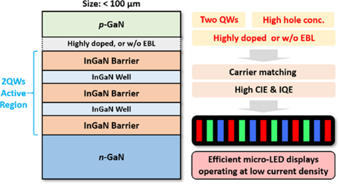
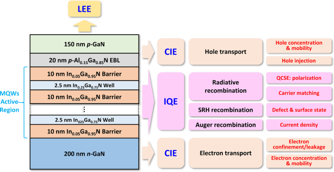
この研究では、60×60μmの長方形のチップサイズと465nm付近のピーク発光波長を持つ青色InGaNマイクロLEDの一般的な構造をシミュレーションに使用します。図1は、青色のマイクロLEDが200 nm n で構成されていることを示しています。 -GaN層、MQWのアクティブ領域、20 nm p -Al 0.15 Ga 0.85 NEBLおよび150nm p -GaN層。 MQWのアクティブ領域は、8、5、3、2、または1周期で構成され、厚さは2.5nmのIn 0.25 Ga 0.75 厚さ10nmのIn 0.05 に埋め込まれたNQW Ga 0.95 N量子バリア(QB)。 MQWのIn組成は、目的の青色発光波長を実現するように調整および最適化されています。 n のドーピング濃度 -GaN、 p -AlGaN EBL、および p -GaNは2×10 18 cm -3 、3×10 18 cm -3 、および1×10 19 cm -3 それぞれ。
LEDの効率のシミュレーションと分析に使用されるInGaN / GaNベースの青色発光ダイオードの概略図
マイクロLEDの光学的および電気的特性は、ソフトウェアAdvanced Physical Model of Semiconductor Devices [37]を使用して数値的に調査されます。シミュレーションでは、自発分極と圧電分極によって引き起こされる界面電荷密度の50%が想定されています[38]。特に明記されている場合を除き、SRHの寿命とオージェ再結合係数は100nsおよび1×10 –31 に設定されています。 cm 6 s -1 、それぞれ[39、40]。バンドオフセット比は0.7 / 0.3 [41]と想定され、光抽出効率は70%に固定され、動作温度は300Kです。シミュレーションで使用される他の材料パラメータは参考文献[42]にあります。
>結果と考察
LEDのウォールプラグ効率(WPE)は、次のように表すことができます。
$$ {\ text {WPE}} =\ frac {{P _ {{{\ text {out}}}}}} {{I _ {{{\ text {op}}}} \ times V}} =\ eta_ {{{\ text {EQE}}}} \ frac {\ hbar \ omega} {{e \ times V}} =\ eta _ {{{\ text {EQE}}}} \ times \ eta _ {{{\ text {elect}}}}、$$(1)ここで P out 光出力パワー I を示します op は動作電流、 V は駆動電圧、ℏω は光子エネルギーであり、η 選出 は電気効率です。 EQE η EQE は電流注入効率(CIE)の積ですη CIE 、IQE η IQE および光抽出効率(LEE)η LEE 、次の方程式で記述されているように:
$$ \ eta _ {{{\ text {EQE}}}} =\ eta _ {{{\ text {CIE}}}} \ times \ eta _ {{{\ text {IQE}}}} \ times \ eta _ {{ {\ text {LEE}}}}。$$(2)さらに、ABCモデル[43]によると、η IQE 次のように表すことができます:
$$ \ eta _ {{{\ text {IQE}}}} =\ frac {{R _ {{{\ text {rad}}}}}} {{R _ {{{\ text {rad}}}} + R_ {{{\ text {SRH}}}} + R _ {{{\ text {Auger}}}}}}、$$(3)ここで R rad は放射再結合率、 R SRH はSRHの非放射再結合率であり、 R オーガー オージェ再結合率です。図1は、さまざまな種類の効率と、関連する物理的なメカニズムおよび要因を示しています。
R rad また、CIEを最大化し、電気効率とLEEを改善し、SRHとAugerの再結合を減らして、低電流密度で動作するマイクロLEDの全体的な効率を改善する必要があります。これらすべての課題に対処するには、システムレベルのアプローチが必要です。光抽出を除いて、これらの課題については次のセクションで説明し、マイクロLEDの効率的なエピタキシャル構造を作成するための潜在的なソリューションも提案します。
低電流密度でのQCSE:内部分極フィールド
偏光誘起QCSEは、窒化物LEDのIQEを制限する主要な要因の1つです[44]。 QCSEは、従来の大型ハイパワーLEDについて広く研究されてきましたが、マイクロLED固有のアプリケーションのコンテキストではまだ十分な議論がありません。したがって、この重要な効果を最初に調査します。ここで説明するマイクロLEDのアクティブ領域は、5周期のQWで構成されています。これは、従来の窒化物LEDで最も一般的に使用されるQW番号です。
図2aは、200および0.1 A / cm 2 での5番目のQWのエネルギーバンド図と、関連する第1レベルの電子および正孔の波動関数を示しています。 。 QBとQWは大きなバンドの曲がりを経験し、電子と正孔の波動関数の空間的分離につながります。さらに、バンドベンディングは低電流密度でより強く、より強いQCSEを示します。この現象は、低い注入電流密度で非平衡キャリアが少ない弱いスクリーニング効果に起因します(追加ファイル1:図S1a-dおよび関連する説明を参照)[41]。図2bは、より厳しいQCSEが低電流密度でのキャリア波動関数の空間的分離を強化し、それがより低い放射再結合率につながることを示しています。偏光効果がある場合とない場合、つまりQCSEがある場合とない場合の放射再結合率とELスペクトルをさらに計算して、電子正孔分離が低電流密度での発光をどのように定量的に低減するかを示します。図2c、dは、放射再結合率とEL強度の積分強度がQCSEによってそれぞれ約84.0%と72.3%減少することを示しています。これらの結果は、低電流密度でのQCSEが強化されているため、マイクロLEDの効率を従来の高出力の組み合わせよりも改善することが難しいことを示しています。
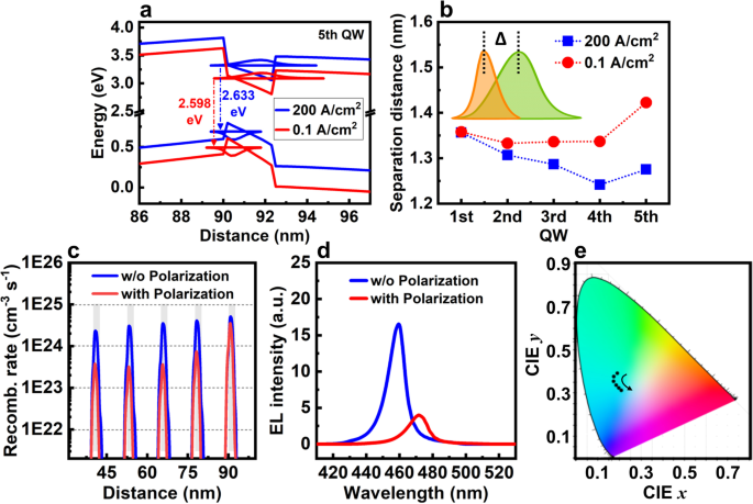
a エネルギーバンド図と、200および0.1 A / cm 2 での5番目のQWの関連する第1レベルの電子および正孔の波動関数 、 それぞれ。 b 200および0.1A / cm 2 での電子と正孔の波動関数のピーク位置の分離距離 、 それぞれ。 c 放射再結合率と d 0.1 A / cm 2 で計算されたELスペクトル それぞれ分極なしと分極あり。 e 電流密度が0.1〜20 A / cm 2 の青、緑、赤のLEDから作成されたカラーポイント 1931-CIE(x、y)色度図にプロット
さらに、さまざまな注入電流密度での発光波長の正確で安定した制御は、明るさ、色の精度、彩度などのさまざまな重要なパラメータを決定するため、マイクロLEDディスプレイにとって重要です。ただし、低電流密度でのより厳しいQCSEは、特により高いインジウム組成を必要とする緑色および赤色のマイクロLEDの場合、これを大きな課題にします。より高いインジウム組成とより強いQCSEを備えたInGaNQWのバンドベンディングの増加の直接的な結果として、遮蔽効果により、波長シフト対電流密度がより顕著になります。さまざまな電流密度のInGaNベースの赤、緑、および青のマイクロLEDのELスペクトルをさらに計算して、スペクトルシフトがディスプレイのカラーポイントにどのように影響するかを示します。追加ファイル1:図S2は、0.1〜20 A / cm 2 であることを示しています。 、ピーク波長の青方偏移は、赤、緑、青のマイクロLEDでそれぞれ約15.8、6.6、1.7nmです。追加ファイル1:表S1に要約されているように、赤、緑、および青のマイクロLEDを組み合わせて作成されたカラーポイントも計算されます。図2eは、対応する1931-CIE(x、y)色度図を示しています。明らかに、電流密度が増加すると、RGBマイクロLEDからの発光の色が緑から青緑に大きく変化しました。 1931-CIE x値は0.1676から0.2084に交差し、1931-CIEy値は0.3891から0.3106に交差します。電流密度に対するカラーポイントのこの大幅な変化は、マイクロLEDディスプレイのパフォーマンスを大幅に低下させます。
多くの報告では、InGaN / AlGaN超薄超格子バリア[45]、GaN中間層バリアを備えたInGaN / GaN / AlGaN / GaN MQW [46]、しわのあるMQW [47]の使用、挿入など、QCSEを抑制するためのいくつかのアプローチが提案されています。 MQWの前のストレインリリーフ層[48]。しかし、QCSEは、 c の固有の特性によって引き起こされます。 -平面窒化物材料。 MQWのいくつかの調整は、この影響を完全に抑制するのに十分ではありません。最近、無極性窒化物LEDでまともな効率が達成されました。非極性GaN基板のコストを削減できれば、非極性LEDは、QCSEを削減し、安定したフルカラー発光を実現するための理想的なソリューションになります[49]。
運送業者の輸送とマッチング
電子( J n )と穴( J p )電流密度は次のように表すことができます:
$$ J_ {n} =\ sigma_ {n} \ left | {\ varvec {E}} \ right | =nq \ mu_ {n} \ left | {\ varvec {E}} \ right |、$$(4)$$ J_ {p} =\ sigma_ {p} \ left | {\ varvec {E}} \ right | =pq \ mu_ {p} \ left | {\ varvec {E}} \ right |、$$(5)ここで、σ n およびσ p 導電率を示します、 n および p 濃度、μ n およびμ p はそれぞれ電子と正孔の移動度であり、 E 電界を示します。窒化物では、正孔濃度は電子より1桁低く[50]、正孔移動度は電子より2桁低くなります[51]。この濃度と移動度の非対称性は、キャリアフラックスの不一致につながります( J n > J p )そして、次の2つの方法でLEDのパフォーマンスを低下させます。
現在の射出効率 :電流注入効率η CIE 再結合電流の比率を表します J リコム 現在の合計 J 合計 、次の式[52]のように:
$$ \ eta _ {{{\ text {CIE}}}} =\ frac {{J _ {{{\ text {recomb}}}}}} {{J _ {{{\ text {total}}}}}} =\ frac {{J _ {{n {\ text {--recomb}}}} + J _ {{p {\ text {--recomb}}}}}} {{J_ {n} + J_ {p}}} =\ frac {{2 \ times J_ {p}}} {{J_ {n} + J_ {p}}}。$$(6)J リコム キャリア電流の小さい方、つまり正孔電流に依存します。式(6)は、キャリアの不一致( J n > J p )CIEの最大化を制限します。
放射再結合率 :放射再結合率 R rad フェルミの黄金律では、次の方程式として記述されます。
$$ R _ {{{\ text {rad}}}} =C \ times \ smallint {\ text {d}} E_ {cv} hv_ {cv} \ left | {\ overline {{M_ {T}}} \ left({E_ {cv}} \ right)} \ right | ^ {2} \ rho_ {r} \ left({E_ {cv}} \ right)f_ { v} \ left({1 --f_ {c}} \ right)、$$(7)ここで C は定数、 E cv は遷移エネルギー、 h プランク定数ν cv は生成された光の周波数です、ρ r は状態密度の減少、 f c および f v はフェルミ-ディラック分布であり、 | M T | 2 は運動量行列要素です[53]。 QWでの正孔の蓄積が少なく、電子の蓄積が増えると、結晶格子が膨張し、引張ひずみが発生する可能性があります。この応力変動の下で、価電子帯の最大値の周りの量子レベルの電荷密度が減少します。これにより、光学遷移確率がさらに低下し、 R が低下します。 rad 式によると。 (7)。このように、単一のQWでのローカルキャリアの不一致もIQEを制限します。このトピックに関するより具体的な議論は、以前のレポート[54,55,56]にあります。
次のセクションでは、QW番号 p の影響 タイプのドーピング濃度、およびキャリア輸送のEBL構造を分析して、最適なキャリアマッチング条件を決定します。最後に、低電流密度で動作する効率的なマイクロLEDディスプレイ用に最適化されたエピタキシャル構造が提案されます。
5QWでのキャリアの不一致
まず、5QWの青色マイクロLEDのキャリア輸送特性をシミュレートします。 200 A / cm 2 でのキャリア濃度の分布 および0.1A / cm 2 追加ファイル1:図S3aおよびbにそれぞれ示されています。 5 QWの不均一な分布は、高電流密度と低電流密度の両方で観察できます。追加ファイル1:図S3cおよびdは、MQW(684 cm 2 )の電子移動度を示しています。 V -1 s -1 )は、穴の移動度(10 cm 2 )よりも2桁高くなります。 V -1 s -1 )。したがって、電子は再結合に関与せずにMQWに注入され、通過する可能性があり、電子漏れの問題と低いCIEにつながります[51]。
図3aは、200 A / cm 2 での電子と正孔の電流密度の分布を示しています。 。総正孔電流密度(217.4 A / cm 2 )は電子のわずか65.2%(333.3 A / cm 2 )、キャリアの深刻な不一致と低いCIEを示します。漏れ電子電流は116.0A / cm 2 と高いです。 、これは放射効率と正孔注入の両方を低下させます。図3bに示すように、漏れ電子電流はわずか0.01 A / cm 2 です。 、および計算されたη CIE 0.1 A / cm 2 で95%もの高さ 。これらの結果は、低電流密度で高いCIEを達成する方が簡単であることを示しています。ただし、 J である5番目のQWを除く p J と等しくすることができます n 、キャリアの不整合と追加の電子蓄積は、高電流密度と低電流密度の両方で、他の4つのQW(QW 1、2、3、および4)で非常に深刻です。 200 A / cm 2 、これら4つのQWの電子電流密度は、正孔電流密度の120、43、16、および5倍です(図3a)。 0.1A / cmで 2 、それらは正孔電流の23、9、4、および2倍です(図3b)。式に基づく。 (7)、この大きなキャリアの不一致は、これら4つのQWの放射再結合率を明らかに低下させます。したがって、これら4つのQWの放射再結合率は、200 A / cm 2 で約3.4%、4.0%、10.1%、および34.2%です。 、および0.1 A / cm 2 で11.3%、10.1%、10.7%、21.2% 5番目のQWと比較して。これらのキャリアの不一致と低放射放射は、最終的にマイクロLEDのモノリシック効率を低下させます。
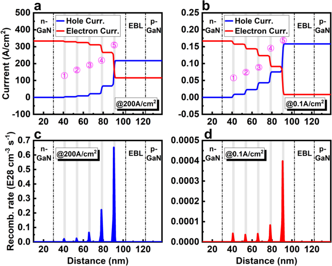
5QWのLEDのキャリア電流分布 a 200A / cmで 2 および b 0.1A / cmで 2 。 5QWのLEDの放射再結合率 c 200A / cmで 2 および d 0.1A / cmで 2
運送業者の輸送とマッチングに影響を与える要因
QW番号 :高電流密度で動作する従来の大型LEDの場合、高い光出力を実現するには、5周期または8周期または10周期のMQWを使用する必要があります。ただし、マイクロLED発光ディスプレイの場合、出力電力ははるかに小さく、動作電流密度ははるかに低くなります。前のセクションで説明したように、低電流密度でも、キャリアの不整合は5QWで非常に深刻なままであり、1つのQWだけが最良の整合条件を達成できます。この観点から、低電流密度で動作するマイクロLEDの場合、QW数が少ないアクティブ領域は、キャリアマッチングが改善されるため、効率を改善するためのより良い設計になるはずです。
マイクロLEDに対するQW数の影響を調査して、仮定を検証します。図4a–fは、0.1 A / cm 2 でのキャリア電流密度と放射再結合率を示しています。 それぞれ3QW、2QW、および1QWのLEDの数。現在の曲線には、交点が1つだけあります(キャリアマッチングが最適な1つの点、 J n = J p )電流の単調減少傾向により、QWが少ない場合、3QWと2QWの場合のように、2つの異なるQWで2つの交点を達成できます(図4a、b)。言い換えると、MQWでのキャリアの不一致は、QWを少なくすることで部分的に克服できます。特に2QWの場合、適切に調整することで、2つのQWすべてでキャリアフラックスの完全一致を実現できます。放射再結合によるキャリア消費は、QWが少ないアクティブ領域に集中するため、放射再結合率も3QWおよび5QWよりも2QWの方が高くなります(図3d、4d、e)。間違いなく、最良のキャリアマッチングは、QWが1つしかないLEDであり、図4c、fに示すように、放射再結合率も1QWで最も高くなります。
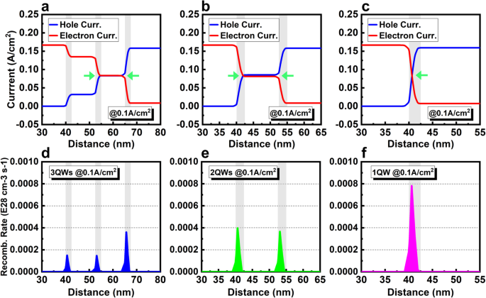
a を使用したLEDのキャリア電流分布 3QW、 b 2QW、および c 0.1 A / cmで1QW 2 。 d のLEDの放射再結合率 3QW、 e 2QW、および f 0.1 A / cmで1QW 2
図5a、bは、0〜200 A / cm 2 の電流密度の関数としてのIQEを示しています。 および0〜10 A / cm 2 、 それぞれ。 50 A / cm 2 を超える電流密度の場合 、QW数が減少すると、IQEは減少します。対照的に、電流密度が約30 A / cm 2 未満のIQE QW数が減少すると増加します。 0.1A / cmで 2 、8、5、3、2、および1 QWのIQE値は、それぞれ55%、62%、69%、77%、および78%です。さらに、図5bに示すように、ピークIQEの位置も6.0 A / cm 2 から移動します。 8QWで最低電流密度約1.2A / cm 2 2QWで。低電流密度(<1A / cm 2 )でのIQE曲線 )また、QW数が少ないほど急勾配でシャープになり、最高の効率をより簡単かつ迅速に達成できることを示します。これは、低電流密度での効率を改善するのに非常に有益です。 IQEのこの傾向の背後にある物理的メカニズムは、キャリアフラックスのより良いマッチング、およびより少ないQW数での活性領域におけるより集中したより強い放射放出によって説明することができます。図5cに示すように、8 QWと比較して、0.1 A / cm 2 での5、3、2、および1QWの積分EL強度 それぞれ約6.1%、14.8%、28.4%、32.1%増加します。この結果は、QW数を減らすことで、効率だけでなく出力電力も向上することを確認しています。
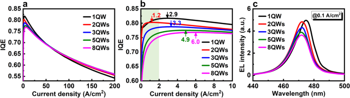
a IQE曲線と b IQEは、8、5、3、2、および1QWのLEDの低電流密度で曲線を描きます。 c 0.1 A / cm 2 で8、5、3、2、および1QWのLEDのELスペクトル
シミュレーション結果は、1QWが最高のEL強度を持ち、低電流密度で動作するマイクロLEDに最適な構造であることを示しています。しかし、実験的には、平坦な表面と鋭い界面を持つ1つのQWだけをエピタキシャル成長させることは困難です。さらに、1QW構造の場合、ピークIQEの位置はわずかに増加して2.9 A / cm 2 、IQE曲線の形状もわずかに変化しました。これは、単一のQWの特別な状況によって説明できます。他のQWと比較して、EBLに隣接するQWは特殊な偏光環境を持っており、「問題のあるQW」と見なされます。このトピックについては、 AlGaN EBL のセクションで詳しく説明します。 。これらの理由を考慮すると、2QWは、キャリアフラックス、IQE値、およびEL強度が1QWに近い、同様の良好なマッチングを備えた最良のアクティブ領域設計である必要があります。したがって、次のセクションでは、すべてのシミュレーションは2QWのマイクロLEDに基づいています。
P-GaNドーピング濃度 :異なる p の2QWLEDのパフォーマンス p のタイプのドーピング濃度 -GaNはさらに調査されます。図6aに示すように、 p のドーピング濃度が -1×10 18 から増加するGaN cm -3 〜5×10 19 cm -3 、0.1 A / cm 2 での放射再結合率 2つのQWでさらに約3.1%と3.0%増加します。図6bは、正孔電流密度の合計が0.157から0.162 A / cm 2 に増加することを示しています。 一方、漏れ電子電流密度は0.009から0.005 A / cm 2 に減少します。 ドーピング濃度の増加に伴い。 n 付近のQWの再結合電流は注目に値します。 -サイドは p 付近のQWよりも高い -側(図6b)。したがって、 n 付近の放射再結合率 -サイドQWも、 p 付近よりもわずかに高くなっています。 -サイドQW。図6cに示すように、電子/正孔の擬フェルミ準位と最高伝導帯または最低価電子帯との間のエネルギー距離として定義されるEBLのキャリアのエネルギー障壁は、異なる場合でもほとんど変化しないことがわかります。 p のドーピング濃度 -GaN, that is, the hole injection is not improved by increasing doping concentration. Figure 6d shows the average hole concentration in the p -GaN and QWs. The hole concentration in the p -GaN is almost exponentially dependent on the doping concentration. Inside the QWs, the hole concentration is increased approximately twice from 1.59 × 10 19 cm -3 to 3.08 × 10 19 cm -3 with a higher doping concentration. These results indicate that the increased hole concentration is the main contribution for the improvement of radiative recombination. Therefore, even at low current density, the p -type doping problem of nitride remains notable, and enhancing the doping efficiency and hole concentration is still beneficial for the efficiency of micro-LED.

a Radiative recombination rates of 2QWs LED with various doping concentrations in p-GaN. b Carrier current distribution with different doping concentrations in p -GaN。 c Enlarged energy band diagrams of EBL with different doping concentrations in p -GaN。 d Average hole concentration in p -GaN and QWs with various doping concentrations of p -GaN
AlGaN EBL :In the last decades, a 10–20 nm p -type AlGaN EBL has become a standard structure for traditional nitride-based LEDs. This EBL is considered to block the electron leakage and suppress the efficiency droop under high injected current density. In spite of this, it is worth noting that the EBL is still a very complicated, subtle structure for the LED. It involves many important factors, including Al composition, p -type doping efficiency of AlGaN, band offset ratios, and polarization effect. Each of them can influence the band structure and carrier transport substantially, then determines the effectiveness of EBL. For the construction of EBL, thickness, composition, and doping concentration must be considered and optimized carefully to balance the enhancement of electron confinement and the blocking of hole injection, otherwise, the opposite may happen, and the performance of LED might deteriorate. For micro-LED, the effectiveness of EBL for operating at low current density must be reconsidered, which may be different with the case of traditional high input/output LED.
a. Doping concentration of EBL :First, the effect of EBL doping concentration on carrier transport at low current density is investigated. The thickness and Al composition of EBL are fixed as 20 nm and 0.15, respectively. Considering the low solubility of Mg dopant in AlGaN, the crystal degradation, and compensation effect by over-doping [50], the doping concentration of EBL is first set as be 3 × 10 18 cm -3 。 Figure 7a shows the corresponding energy band structure. Clearly, despite the existence of EBL, the electron leakage out of the QW still can be caused by the insufficient electron confinement due to the downward bending of the last QW and EBL. A new energy valley under the electron quasi-Fermi level appears at the interface of last QB and EBL. Thus, electrons would escape from QW and accumulate in this area. This distortion of band structure makes the EBL relatively ineffective, and it can be contributed to the polarization effect. As shown in Fig. 7c, the strong polarization induces a large amount of charges at the interfaces. Due to the unbalanced polarization charges are positive at the interface of the last QB/EBL, a large electrostatic field pointing from the p -side to the n -side builds up in the last QB, which is opposite to the fields in other QBs and EBL. These electrostatic fields pull down the energy band of the last QB and EBL. Moreover, the electric fields in the last QW and last QB both can attract electrons and drive them out of the active region into the p -layer. This can be observed in the carrier concentration diagram, as shown in Fig. 7d. The dotted black line indicates that a part of the electrons escape from the active region and accumulate at the interface of last QB/EBL. In the EBL and p -GaN, the leakage electron remains relatively high.

Energy band diagrams of 2QWs LED with a 3 × 10 18 cm -3 および b 6 × 10 19 cm -3 doping concentration in AlGaN EBL. c Space charge density and d carrier concentration distribution of 2QWs LED with 3 × 10 18 and 6 × 10 19 cm -3 doping concentration of EBL. The inset of c shows the direction of polarization fields
On the other hand, the EBL also introduces a potential barrier as high as 480 meV for hole injection. Moreover, as shown in Fig. 7a, c, an energy valley close to the hole quasi-Fermi level appears at the interface region between the EBL/p -GaN due to the polarization effect. As indicated by the solid black line of Fig. 7d, most of the holes are blocked by the EBL and thus, accumulate at the energy valley of the EBL/p -GaN interface. Owing to this inefficient carrier transport, the last QW is considered as a “problem QW,” and the EBL only has a low capability for electron confinement, and should be responsible for the poor hole injection. Compared with the traditional high input/output LED, this polarization induced ineffectiveness of the EBL function could be particularly severe for the micro-LED due to the enhanced polarization effect by less carrier screening at low current density.
Band engineering by increasing the doping concentration of EBL is a possible method to improve the electron confinement and hole injection. The activation energy of Mg dopant in AlGaN EBL is higher than GaN, therefore, even under a similar doping concentration, the active hole concentration in EBL remains much lower than p -GaN。 The lower hole concentration could further separate the hole quasi-Fermi level and valence band, then increase barrier height. Based on this analysis, the doping concentration of EBL needs to be much higher than p -GaN。 Considering the doping limitation in actual experiment, 6 × 10 19 cm -3 is selected as a new doping concentration in the EBL. As shown in Fig. 7b, by increasing the doping concentration, the valence band of EBL is lifted due to the alignment of hole quasi-Fermi level, resulting in a reduced hole energy barrier of 281 meV. Moreover, the high p -type doping also helps lower the electron quasi-Fermi level with respect to the conduction band in EBL, hence increasing the effect barrier for electron leakage to 1175 meV. These changes improve electron confinement and hole injection. Figure 7d shows that compared with the doping concentration of 3 × 10 18 cm -3 , the hole concentration in the active region is greatly increased, and the leakage electron in the EBL and p -GaN is reduced to almost zero. However, the energy valley at the interface between the EBL/p -GaN still exists. Moreover, the upward of valence band also introduces a new energy valley for the hole accumulation at the interface between the last QB/EBL, which can be confirmed by the hole concentration distribution in Fig. 7d. These energy valleys can impede the hole injection into QWs, hence compensating the advantage of high doping concentration.
b. Al composition of EBL :Compared with the increase of doping concentration, reducing the composition of AlGaN EBL may be an easier, more efficient method to improve the carrier transport at low current density. The effectiveness of EBL is sensitively dependent on Al composition, band offset, and polarization effect. Increasing the Al composition of EBL can increase the band offset between the last QB/EBL, which increases the electron barrier height. However, as shown in Fig. 8a, the polarization-induced charges at the interfaces also increase accordingly, which pull down the electron barrier height. Two mechanisms have the opposite effect for confining electrons.

a Space charge density distribution of 2QWs LED with different EBL. The inset shows the direction of polarization field. Energy band diagrams of 2QWs LED b with Al0.1 Ga0.9 N EBL and c without EBL. d Carrier concentration distribution, e carrier current density, f IQE and g EL spectra of 2QWs LED with different EBL. The inset of g shows the working voltages at 0.1 and 1 A/cm 2 with different EBLs
Based on this analysis, the carrier transport of 2QWs micro-LEDs with different EBL structures at 200 and 0.1 A/cm 2 are investigated. The result of effective energy barrier heights of different EBL are summarized in Table 1. First of all, both the electron and hole energy barriers at low current density are much higher than the cases of at high current density due to the lower nonequilibrium carrier population. A higher energy barrier can improve the electron confinement, but also severely impedes the hole injection at low current density. This indicates that the influence of EBL on the carrier transport of micro-LED operating at low current density is much higher than that of the traditional high input/output LED. Table 1 also shows that with a relatively low Al composition in EBL, the electron barrier decreases with Al composition increased, which indicates that the downward of conduction band induced by polarization effect is larger than the increased band offset introduced by the higher Al composition. By further increasing the composition, the electron barrier increases along with composition, meaning that the band offset becomes dominant over the polarization effect. Compared with high current density, this turning point of composition is higher at low current density due to the enhanced polarization effect by less carrier screening. On the other hand, because of the original band offset between the last QB/p -GaN and the band bending, there are energy barriers for electron and holes exist at the interface even without the EBL. At 200 A/cm 2 , when the composition is lower than 0.20, the electron energy barrier is lower than the case of without EBL, but the hole barrier is higher approximately 64 meV. At 0.1 A/cm 2 , even with composition higher than 0.20, the electron barrier of AlGaN EBL (523 meV) is still 151 meV lower than the case of without EBL (674 meV), but the hole barrier is increased approximately 76 meV from 409 to 485 meV. These results indicate that both the electron confinement and hole injection could be deteriorated by the EBL with an incorrect composition, especially for micro-LED operating at low current density.
<図>For a deep analysis, band structures of micro-LEDs with Al0.10 Ga0.90 N EBL and without EBL as representatives are illustrated in Fig. 8b, c. The EBL introduces two energy valleys at the interface of last QB/EBL and EBL/p -GaN for electron and hole accumulation, respectively, which can be confirmed by the carrier concentration diagram in Fig. 8d. Therefore, the electron confinement and hole injection are poor for this structure. When the EBL is removed, as shown in Fig. 8c, the energy barrier for electron is increased, and the energy valley for electron extracting and accumulation disappeares. These changes prevent electrons leakage more effectively, as confirmed in Fig. 8d. Meanwhile, the barrier height for hole injection is reduced, and the energy valley at the EBL/p-GaN interface is also removed. So, the hole can transport directly into the QW without facing large obstacle, as shown in Fig. 8c, d.
The above careful investigation suggests that without EBL may be a better structure for the micro-LED operating at low current density. Simulation results support our suggestion. Figure 8e illustrates the carrier current density at 0.1 A/cm 2 with different EBL structures. When the Al composition of the EBL is reduced from 0.15 to 0.04, the total electron and hole current densities increase from 0.167 and 0.159 A/cm 2 to 0.225 and 0.225 A/cm 2 、 それぞれ。 Moreover, when the EBL is completely removed, both the total electron and total hole current densities greatly increase to 0.528 A/cm 2 , which is approximately 3 times higher compared with the Al0.15 Ga 0.85 N EBL. This enhancement is contributed to the improved electron confinement and hole injection.
Figure 8f shows the IQE curves at low current density. When the Al composition of EBL is reduced from 0.15 to 0.04, the IQE values increase evidently due to the improved carrier transport. However, by removing the EBL, the IQE value experiences a slight decrease compared with Al0.04 Ga0.96 N EBL. This can be explained by the carrier matching in two QWs. As indicated by the green arrows in Fig. 8e, a, perfect carrier matching occurred in both the two QWs with Al0.04 Ga0.96 N EBL. With the increase of current density by removing EBL, the matching of electron and hole flux has been slightly broken in the first QW, where the electron current density is slightly higher than the hole. Therefore, the IQE is slightly reduced because of this carrier mis-matching in one QW.
The superiority of micro-LED without EBL is still remarkable due to the improved carrier transport. As shown in Fig. 8g, at 0.1 A/cm 2 , the integral EL intensities of micro-LED without EBL are 3.53, 3.23, and 2.38 times higher compared with the LED with Al0.15 Ga 0.85 N, Al0.10 Ga0.90 N and Al0.04 Ga0.96 N EBL, respectively. Moreover, as shown in the inset of Fig. 8g, the working voltages under 1 A/cm 2 and 0.1 A/cm 2 are reduced about 0.53 V and 0.57 V by removing the EBL, respectively. This improves the electrical efficiency, then finally increases the WPE of micro-LED. To further confirm that the EBL-free structure is a better design for micro-LED operating at low current density, another simulation is performed using the reported blue micro-LED structure with maximal known efficiency. The results and discussions can be found in the Supporting Materials (Additional file 1:Fig. S4a-d).
Optimized Structure for Micro-LED Operating at Low Current Density
Based on above simulation and analysis, the optimized epitaxial structure specifically designed for the efficient micro-LED emissive display operating at low current density is proposed, as shown in Fig. 9. Three principles must be followed. First, in contrast to the traditional large-size high-power nitride LED, the QW number of micro-LED should be reduced to just two, which has a better condition for the carrier matching, a more concentrated radiative emission, and higher IQE and WPE. Second, the p -type doing still needs to be enhanced due to the relatively low hole concentration and mobility compared with the electron in nitride, which demands a more efficient p -type doping strategy. Third, to improve the carrier transport and matching, the doping concentration of AlGaN EBL should be greatly enhanced, or the AlGaN EBL can be completely removed. Without using the AlGaN EBL, the electron confinement, hole injection, carrier matching, IQE, and WPE of the micro-LED can be greatly improved at low current density.

Schematic illustration of the optimized epitaxial structure designed specifically for the micro-LED emissive displays operating at low current density
Auger Recombination and SRH Non-radiative Recombination
式に基づく。 (3), except for radiative recombination, the SRH and Auger recombination also play critical roles in the IQE of LED. Hence, it is important to investigate the effects and mechanism regarding the SRH and Auger recombination for the micro-LED. In this part, the LED structure with 2QWs is still used, and all the simulation parameters are the same as mentioned in the Methods except for SRH lifetimes.
Negligible Auger and Prominent SRH Recombination
The SRH recombination rate can be expressed as follows [57]:
$$R_{{{\text{SRH}}}} =\frac{{np - n_{i}^{2} }}{{\tau_{p} \left( {n + n_{i} \exp \left( {\frac{{E_{T} }}{kT}} \right)} \right) + \tau_{n} \left( {p + n_{i} \exp \left( {\frac{{E_{T} }}{kT}} \right)} \right)}},$$ (8) $$\tau_{p} =\frac{1}{{c_{p} N_{t} }}, \tau_{n} =\frac{1}{{c_{n} N_{t} }},$$ (9) $$c_{p} =\sigma_{p} \nu_{p} , c_{n} =\sigma_{n} \nu_{n} ,$$ (10)ここで n i is the intrinsic carrier concentration, τ p およびτ n are the hole and electron SRH lifetimes, respectively, E T is the energy difference between the trap level and the intrinsic Fermi level, c p および c n are the capture coefficients for electron and hole, N t is the trap density, σ p およびσ n are capture cross sections for electron and hole, and ν p およびν n are the average thermal velocities of electron and hole, respectively.式によると。 (8)-(10), the SRH recombination of a trap is completely specified by its density, capture cross sections and energy level.
The Auger recombination rate is given by the following:
$$R_{{{\text{Auger}}}} =\left( {C_{n} n + C_{p} p} \right)\left( {np - n_{i}^{2} } \right),$$ (11)ここで C n および C p are the Auger recombination coefficients.
Given that the injected hole and electron concentrations are much higher than the intrinsic carrier concentration in the undoped QWs (according to simulation result, the highest carrier concentration in QW is only approximately 10 7 cm -3 in the absence of externally injected current), the SRH and Auger recombination rate can be further simplified as the following equations:
$$R_{{{\text{SRH}}}} =\frac{np}{{\tau_{p} n + \tau_{n} p}},$$ (12) $$R_{{{\text{Auger}}}} =\left( {C_{n} n + C_{p} p} \right)np.$$ (13)Equations (12) and (13) clearly show that R SRH is in direct proportion to the first power of the carrier concentration, but R Auger depends on the third power of the carrier concentration, that is, R SRH is sensitive to low current density, while the R Auger is more dominant at high current density.
This theoretical analysis agrees with our simulation results. Figure 10a, b shows the calculated radiative, SRH, and Auger recombination rates at 200 and 0.1 A/cm 2 、 それぞれ。 At high current density, the Auger recombination rate (about 0.8–1.4 × 10 29 cm -3 s -1 ) is comparable wiht the radiative rate (about 4.2–6.0 × 10 29 cm -3 s -1 )。 In fact, the substantial problem of efficiency droop at high drive currents is now widely acknowledged as caused by the Auger recombination [20]. While, at low current density, relatively, the Auger recombination rate dramatically decreases to two orders of magnitude lower (about 6.3–7.2 × 10 22 cm -3 s -1 ) than the radiative recombination (about 3.7–4.0 × 10 24 cm -3 s -1 )。 Therefore, the Auger recombination should be negligible at low current density. Conversely, with the decrease of current density, the SRH recombination rate relatively increases from a small value at 200 A/cm 2 (two orders of magnitude lower than radiative recombination) to a level comparable with the radiative emission at 0.1 A/cm 2 。 As a result, the micro-LED operating at low current density requires improvement in the SRH or defect recombination instead of the Auger recombination.

Radiative, SRH, and Auger recombination rates of 2QWs LED a at 200 A/cm 2 および b at 0.1 A/cm 2 。 c SRH/Radiative ratio with various SRH lifetimes at 200 and 0.1 A/cm 2 。 d IQE values at 200 and 0.1 A/cm 2 、 e IQE curves with large current density and f IQE curves with low current density at various SRH lifetimes
Requirement for Low Defect Density
式によると。 (9), SRH lifetimes, τ p およびτ n , are in inverse proportion to the density of defects N t 。 Therefore, the effect of defect density can be estimated by simply changing the SRH lifetime in the simulation. Figure 10c shows the calculated ratio of SRH/radiative recombination rate at various SRH lifetimes. With the decrease of SRH lifetimes from 150 to 50 ns, i.e., the increase of defect density, the SRH/radiative ratio slightly increases from 0.01 to 0.03 at 200 A/cm 2 , but greatly increases from 0.15 to 0.43 at 0.1 A/cm 2 。 This means that a much larger percentage of carriers is consumed by the trapping defects at low current density. Therefore the efficiency is much more sensitive to the defect density at low current than high current density. The IQE results as shown in Fig. 10d, e confirm this trend. With the decrease of SRH lifetimes from 150 to 50 ns, IQE only decreases about 0.01 at 200 A/cm 2 , but dramatically decreases about 0.17 at 0.1 A/cm 2 。 Moreover, as shown in Fig. 10f, with the decrease of SRH lifetime, the position of peak IQE also moves from 3.1 A/cm 2 to a higher current density of 9.0 A/cm 2 , and the IQE curves become less steep and sharp, which means that the threshold/onset current is increased. This is disadvantageous for improving the efficiency of micro-LED at low current density.
Compared with the traditional large-size high-power LED working at high current density, the micro-LED operating at low current density is much more sensitive to defect density, and minimizing the defect recombination is of paramount importance for achieving a high efficiency. Therefore, the micro-LED requires a much more higher crystal quality of materials than the traditional LED, and poses large challenges for the epitaxial growth of the material and the fabrication of the device for the community.
結論
In summary, the operating behaviors, mechanisms and conditions of InGaN micro-LED operating at low current density are numerically investigated, and an optimized epitaxial structure specifically designed for the micro-LED display is proposed. Analysis of the polarization effect shows that micro-LED suffers a severer QCSE at low current density. Hence, improving the efficiency and controlling the emission color point are more difficult. Carrier transport and matching are analyzed to determine the operating conditions of micro-LED. It is shown that less QW number can improves the carreir matching and leads to higher efficiency and output power at low current density. Effectiveness of the EBL for micro-LED is analyzed, and electron confinement and hole injection are found to be improved simultaneously at low current density by removing the EBL. Moreover, simulaiton has shown that the Auger recombination is negligible, but the SRH recombination greatly influences the efficiency of micro-LED at low current density, which has raised higher requirements for the crystal quality of materials and the fabrication process of devices. Our numerical study can provide valuable guidance for creating efficient micro-LED display and promote future research in this area.
データと資料の可用性
現在の作業のデータと分析は、合理的な要求に応じて対応する著者から入手できます。
略語
- Micro-LED:
-
Micro-light-emitting-diode
- QCSE:
-
Quantum-confined Stark effect
- EBL:
-
Electron blocking layer
- SRH:
-
Shockley–Read–Hall
- LCD:
-
Liquid–crystal display
- OLED:
-
Organic light-emitting diode
- TV:
-
Televisions
- VR:
-
Virtual reality
- AR:
-
Augmented reality
- QW:
-
Quantum well
- MQW:
-
複数の量子井戸
- EQE:
-
外部量子効率
- IQE:
-
内部量子効率
- QB:
-
Quantum barrier
- WPE:
-
ウォールプラグの効率
- CIE:
-
Current injection efficiency
- LEE:
-
光抽出効率
ナノマテリアル
- Zynqベースの設計の協調シミュレーション
- 癌治療のためのナノ粒子:現在の進歩と課題
- 構造的および光学的性質を改善するためのH2 / NH3混合ガス中のGaNベースの多重量子井戸の原子転位
- 効率的な光触媒水素生成のためのS、N共ドープグラフェン量子ドット/ TiO2複合材料
- スーパーキャパシターの電極材料としての階層的多孔質構造を持つ単分散カーボンナノスフェア
- 低消費電力基板発光DFB量子カスケードレーザー
- 高いMgドーピング効率のために特別に設計された超格子p型電子ブロッキング層を備えたほぼ効率の低いAlGaNベースの紫外線発光ダイオード
- 柔軟な繊維状色素増感太陽電池の光電変換効率の改善
- あなたのビジネスのための灯油効率を改善するためのヒント
- 回転効率のためにチームを組む
- 食品製造効率を向上させるための6つのヒント