


assign を使用した組み合わせロジック
verilog の assign ステートメントは、通常、wire の信号を継続的に駆動するために使用されます。 データ型であり、組み合わせロジックとして合成されます。 assign を使用したその他の設計例を次に示します。
例 #1 :シンプルな組み合わせロジック
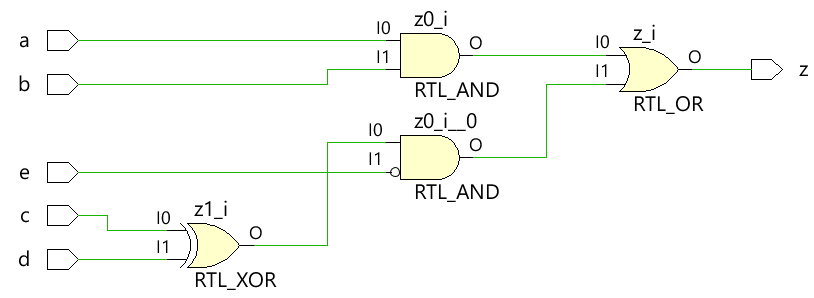
以下に示すコードは、assign で連続的に駆動される出力ワイヤ z を持つ単純なデジタル組み合わせロジックを実装します。 デジタル式を実現するステートメント
module combo ( 	input 	a, b, c, d, e,
								output 	z);

	assign z = ((a & b) | (c ^ d) & ~e);

endmodule
モジュール コンボ 合成ツールを使用して次のハードウェア回路図に精緻化され、組み合わせロジックがデジタル ゲートで実装されていることがわかります。
テストベンチ
テストベンチは、デザインが期待どおりに動作することを確認するためにデザインをシミュレートするためのプラットフォームです。入力のすべての組み合わせは、for を使用して設計モジュールに駆動されます。 新しい値がしばらくしてから入力に適用されるように、10 時間単位の遅延ステートメントでループします。
module tb;
	// Declare testbench variables
  reg a, b, c, d, e;
  wire z;
  integer i;

  // Instantiate the design and connect design inputs/outputs with
  // testbench variables
  combo u0 ( .a(a), .b(b), .c(c), .d(d), .e(e), .z(z));

  initial begin
  	// At the beginning of time, initialize all inputs of the design
  	// to a known value, in this case we have chosen it to be 0.
    a <= 0;
    b <= 0;
    c <= 0;
    d <= 0;
    e <= 0;

    // Use a $monitor task to print any change in the signal to
    // simulation console
    $monitor ("a=%0b b=%0b c=%0b d=%0b e=%0b z=%0b",
              a, b, c, d, e, z);

    // Because there are 5 inputs, there can be 32 different input combinations
    // So use an iterator "i" to increment from 0 to 32 and assign the value
    // to testbench variables so that it drives the design inputs
    for (i = 0; i < 32; i = i + 1) begin
      {a, b, c, d, e} = i;
      #10;
    end
  end
endmodule
シミュレーションログ ncsim> run a=0 b=0 c=0 d=0 e=0 z=0 a=0 b=0 c=0 d=0 e=1 z=0 a=0 b=0 c=0 d=1 e=0 z=1 a=0 b=0 c=0 d=1 e=1 z=0 a=0 b=0 c=1 d=0 e=0 z=1 a=0 b=0 c=1 d=0 e=1 z=0 a=0 b=0 c=1 d=1 e=0 z=0 a=0 b=0 c=1 d=1 e=1 z=0 a=0 b=1 c=0 d=0 e=0 z=0 a=0 b=1 c=0 d=0 e=1 z=0 a=0 b=1 c=0 d=1 e=0 z=1 a=0 b=1 c=0 d=1 e=1 z=0 a=0 b=1 c=1 d=0 e=0 z=1 a=0 b=1 c=1 d=0 e=1 z=0 a=0 b=1 c=1 d=1 e=0 z=0 a=0 b=1 c=1 d=1 e=1 z=0 a=1 b=0 c=0 d=0 e=0 z=0 a=1 b=0 c=0 d=0 e=1 z=0 a=1 b=0 c=0 d=1 e=0 z=1 a=1 b=0 c=0 d=1 e=1 z=0 a=1 b=0 c=1 d=0 e=0 z=1 a=1 b=0 c=1 d=0 e=1 z=0 a=1 b=0 c=1 d=1 e=0 z=0 a=1 b=0 c=1 d=1 e=1 z=0 a=1 b=1 c=0 d=0 e=0 z=1 a=1 b=1 c=0 d=0 e=1 z=1 a=1 b=1 c=0 d=1 e=0 z=1 a=1 b=1 c=0 d=1 e=1 z=1 a=1 b=1 c=1 d=0 e=0 z=1 a=1 b=1 c=1 d=0 e=1 z=1 a=1 b=1 c=1 d=1 e=0 z=1 a=1 b=1 c=1 d=1 e=1 z=1 ncsim: *W,RNQUIE: Simulation is complete.
例 #2:半加算器
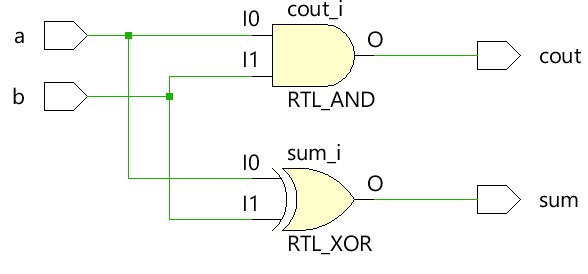
半加算器モジュールは、2 つのスカラー入力 a と b を受け入れ、組み合わせロジックを使用して出力の合計と桁上げビット cout を割り当てます。合計は a と b 間の XOR によって駆動され、キャリー ビットは 2 つの入力間の AND によって取得されます。
module ha ( input 	a, b,
						output	sum, cout);

	assign sum  = a ^ b;
	assign cout = a & b;
endmodule
テストベンチ
module tb;
	// Declare testbench variables
  reg a, b;
  wire sum, cout;
  integer i;

  // Instantiate the design and connect design inputs/outputs with
  // testbench variables
  ha u0 ( .a(a), .b(b), .sum(sum), .cout(cout));

  initial begin
  	// At the beginning of time, initialize all inputs of the design
  	// to a known value, in this case we have chosen it to be 0.
    a <= 0;
    b <= 0;

    // Use a $monitor task to print any change in the signal to
    // simulation console
    $monitor("a=%0b b=%0b sum=%0b cout=%0b", a, b, sum, cout);

    // Because there are only 2 inputs, there can be 4 different input combinations
    // So use an iterator "i" to increment from 0 to 4 and assign the value
    // to testbench variables so that it drives the design inputs
    for (i = 0; i < 4; i = i + 1) begin
      {a, b} = i;
      #10;
    end
  end
endmodule
シミュレーションログ ncsim> run a=0 b=0 sum=0 cout=0 a=0 b=1 sum=1 cout=0 a=1 b=0 sum=1 cout=0 a=1 b=1 sum=0 cout=1 ncsim: *W,RNQUIE: Simulation is complete.

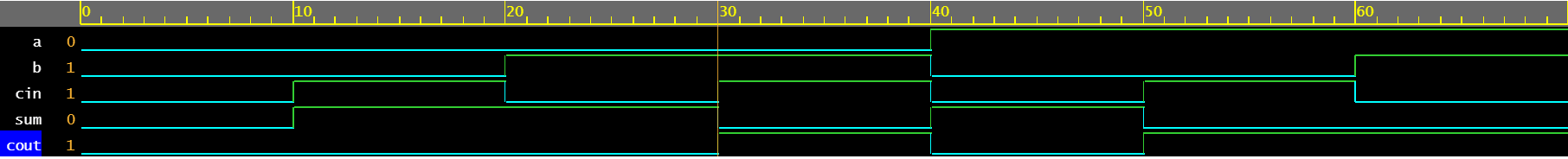
例 #3:全加算器
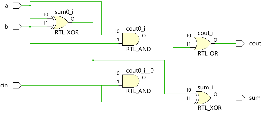
上記の半加算器モジュールを使用して全加算器を構築するか、assign を使用して組み合わせロジック全体をそのまま適用できます。 出力 sum と cout を駆動するステートメント。
module fa (	input 	a, b, cin,
						output 	sum, cout);

	assign sum  = (a ^ b) ^ cin;
	assign cout = (a & b) | ((a ^ b) & cin);
endmodule
テストベンチ
module tb;
  reg a, b, cin;
  wire sum, cout;
  integer i;

  fa u0 ( .a(a), .b(b), .cin(cin), .sum(sum), .cout(cout));

  initial begin
    a <= 0;
    b <= 0;

    $monitor("a=%0b b=%0b cin=%0b sum=%0b cout=%0b", a, b, cin, sum, cout);

    for (i = 0; i < 7; i = i + 1) begin
      {a, b, cin} = i;
      #10;
    end
  end
endmodule
シミュレーションログ ncsim> run a=0 b=0 cin=0 sum=0 cout=0 a=0 b=0 cin=1 sum=1 cout=0 a=0 b=1 cin=0 sum=1 cout=0 a=0 b=1 cin=1 sum=0 cout=1 a=1 b=0 cin=0 sum=1 cout=0 a=1 b=0 cin=1 sum=0 cout=1 a=1 b=1 cin=0 sum=0 cout=1 ncsim: *W,RNQUIE: Simulation is complete.
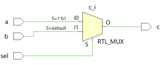
例 #4:2x1 マルチプレクサ
単純な 2x1 マルチプレクサは、三項演算子を使用して、どの入力を出力 c に割り当てるかを決定します。 sel が 1 の場合、出力は a によって駆動され、sel が 0 の場合、出力は b によって駆動されます。
module mux_2x1 (input 	a, b, sel,
								output 	c);

	assign c = sel ? a : b;
endmodule
テストベンチ
module tb;
	// Declare testbench variables
  reg a, b, sel;
  wire c;
  integer i;

  // Instantiate the design and connect design inputs/outputs with
  // testbench variables
  mux_2x1 u0 ( .a(a), .b(b), .sel(sel), .c(c));

  initial begin
  	// At the beginning of time, initialize all inputs of the design
  	// to a known value, in this case we have chosen it to be 0.
    a <= 0;
    b <= 0;
    sel <= 0;

    $monitor("a=%0b b=%0b sel=%0b c=%0b", a, b, sel, c);

    for (i = 0; i < 3; i = i + 1) begin
      {a, b, sel} = i;
      #10;
    end
  end
endmodule
シミュレーションログ ncsim> run a=0 b=0 sel=0 c=0 a=0 b=0 sel=1 c=0 a=0 b=1 sel=0 c=1 ncsim: *W,RNQUIE: Simulation is complete.

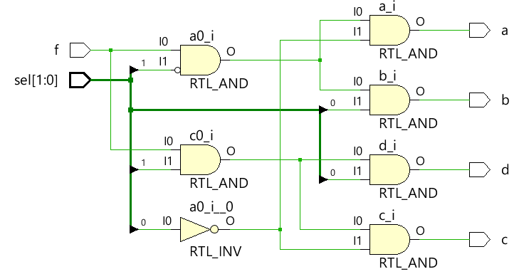
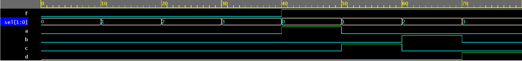
例 #5:1x4 デマルチプレクサ
デマルチプレクサは、sel 入力と f 入力の組み合わせを使用して、さまざまな出力信号を駆動します。各出力信号は個別の assign によって駆動されます 声明。通常、同じ信号を異なる assign で駆動することは推奨されないことに注意してください。
module demux_1x4 (	input 				f,
										input [1:0]	 	sel,
										output 				a, b, c, d);

	assign a = f & ~sel[1] & ~sel[0];
	assign b = f &  sel[1] & ~sel[0];
	assign c = f & ~sel[1] &  sel[0];
	assign d = f &  sel[1] &  sel[0];

endmodule
テストベンチ
module tb;
	// Declare testbench variables
  reg f;
  reg [1:0] sel;
  wire a, b, c, d;
  integer i;

  // Instantiate the design and connect design inputs/outputs with
  // testbench variables
  demux_1x4 u0 ( .f(f), .sel(sel), .a(a), .b(b), .c(c), .d(d));

  // At the beginning of time, initialize all inputs of the design
  // to a known value, in this case we have chosen it to be 0.
  initial begin
    f <= 0;
    sel <= 0;

    $monitor("f=%0b sel=%0b a=%0b b=%0b c=%0b d=%0b", f, sel, a, b, c, d);

    // Because there are 3 inputs, there can be 8 different input combinations
    // So use an iterator "i" to increment from 0 to 8 and assign the value
    // to testbench variables so that it drives the design inputs
    for (i = 0; i < 8; i = i + 1) begin
      {f, sel} = i;
      #10;
    end
  end
endmodule
シミュレーションログ ncsim> run f=0 sel=0 a=0 b=0 c=0 d=0 f=0 sel=1 a=0 b=0 c=0 d=0 f=0 sel=10 a=0 b=0 c=0 d=0 f=0 sel=11 a=0 b=0 c=0 d=0 f=1 sel=0 a=1 b=0 c=0 d=0 f=1 sel=1 a=0 b=0 c=1 d=0 f=1 sel=10 a=0 b=1 c=0 d=0 f=1 sel=11 a=0 b=0 c=0 d=1 ncsim: *W,RNQUIE: Simulation is complete.
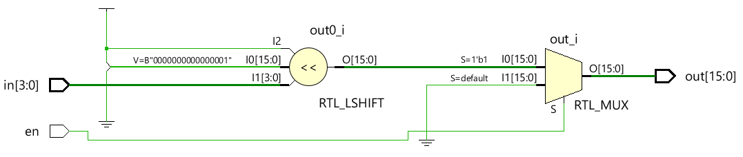
例 #6:4x16 デコーダー
module dec_3x8 ( 	input 					en,
									input 	[3:0] 	in,
									output  [15:0] 	out);

	assign out = en ? 1 << in: 0;
endmodule
テストベンチ
module tb;
  reg en;
  reg [3:0] in;
  wire [15:0] out;
  integer i;

  dec_3x8 u0 ( .en(en), .in(in), .out(out));

  initial begin
    en <= 0;
    in <= 0;

    $monitor("en=%0b in=0x%0h out=0x%0h", en, in, out);

    for (i = 0; i < 32; i = i + 1) begin
      {en, in} = i;
      #10;
    end
  end
endmodule
シミュレーションログ ncsim> run en=0 in=0x0 out=0x0 en=0 in=0x1 out=0x0 en=0 in=0x2 out=0x0 en=0 in=0x3 out=0x0 en=0 in=0x4 out=0x0 en=0 in=0x5 out=0x0 en=0 in=0x6 out=0x0 en=0 in=0x7 out=0x0 en=0 in=0x8 out=0x0 en=0 in=0x9 out=0x0 en=0 in=0xa out=0x0 en=0 in=0xb out=0x0 en=0 in=0xc out=0x0 en=0 in=0xd out=0x0 en=0 in=0xe out=0x0 en=0 in=0xf out=0x0 en=1 in=0x0 out=0x1 en=1 in=0x1 out=0x2 en=1 in=0x2 out=0x4 en=1 in=0x3 out=0x8 en=1 in=0x4 out=0x10 en=1 in=0x5 out=0x20 en=1 in=0x6 out=0x40 en=1 in=0x7 out=0x80 en=1 in=0x8 out=0x100 en=1 in=0x9 out=0x200 en=1 in=0xa out=0x400 en=1 in=0xb out=0x800 en=1 in=0xc out=0x1000 en=1 in=0xd out=0x2000 en=1 in=0xe out=0x4000 en=1 in=0xf out=0x8000 ncsim: *W,RNQUIE: Simulation is complete.

Verilog