


アプリケーションのためのカーボンナノチューブの組み立てと統合
要約
カーボンナノチューブ(CNT)は、高い機械的強度、大きなアスペクト比、高い表面積、明確な光学特性、高い熱伝導率および電気伝導率などの特性の独自の組み合わせにより大きな関心を集めており、エレクトロニクス(トランジスター、エネルギー生産および貯蔵)からバイオテクノロジー(イメージング、センサー、アクチュエーターおよび薬物送達)および他のアプリケーション(ディスプレイ、フォトニクス、複合材料および多機能コーティング/フィルム)までの分野。 CNTの制御された成長、組み立て、統合は、現在および将来のナノチューブアプリケーションの実用化に不可欠です。このレビューは、さまざまなアプリケーションのCNTアセンブリと統合の分野におけるこれまでの進歩に焦点を当てています。先端成長および基部成長モデルの詳細を含む、アーク放電、レーザーアブレーション、および化学蒸着(CVD)に基づくCNT合成が最初に紹介されます。次に、触媒コンディショニング、クローニング、シードベース、テンプレートベースの成長などの方法を使用したCNT構造制御(キラリティー、直径、接合部)の進歩を詳細に調査し、その後、選択的表面化学、ゲルクロマトグラフィーを使用した成長後のCNT精製技術を検討します。密度勾配遠心分離。フォトリソグラフィー、転写印刷、およびインクジェット印刷、誘電泳動(DEP)、スピンなどのさまざまなソリューションベースの技術を使用したさまざまな基板への位置合わせ/配置とともに、触媒のパターン化、森林成長、複合材料に基づく複数のCNTのさまざまなアセンブリおよび統合技術を検討します。コーティング。最後に、エネルギー貯蔵、トランジスタ、組織工学、ドラッグデリバリー、電子暗号化キー、センサーなどの分野でのCNTの現在および新たなアプリケーションにおける課題のいくつかを検討します。
はじめに
カーボンナノチューブ(CNT)は、グラファイトシート(別名グラフェン)でできた長い中空の円筒形の管状構造で、直径は1nm未満から10snmの範囲です[1]。 CNTは、これらのグラフェン層がシリンダーに巻かれる方法に基づいて、さまざまな電子特性を示します。ナノチューブは、単層カーボンナノチューブ(SWCNT)と呼ばれる単層構造である場合もあれば、多層カーボンナノチューブ(MWCNT)と呼ばれる多くの壁を持つ場合もあります。 SWCNTは、電気的に半導体と金属のSWCNT(s-SWCNTとm-SWCNT)にさらに分類できますが、MWCNTは主に金属の挙動を示します。低コスト、軽量、高アスペクト比と表面積、明確な光学特性、高い熱伝導率と電気伝導率、高い機械的強度など、CNTの斬新で有用な特性により、CNTは幅広い電子機器に適しており、興味深いものになっています。 、生物医学およびその他の産業用アプリケーション。たとえば、CNTは、将来の集積回路のアクティブデバイスおよび相互接続として「CMOSを超えた」電子機器に有望です[2]。
CNTはフラーレンファミリーの一部であり、中空球、楕円体、円筒形のチューブなどのケージのような構造の形で原子が結合した炭素同素体のグループです[3]。フラーレンは、六角形と五角形のリングが結合したグラフェンシートで構成されており、湾曲した構造になっています。グラフェンは炭素の同素体であり、2次元の六角形の格子に配置された炭素原子の単層で構成されています。これは半金属であり、価電子帯と伝導帯の間にオーバーラップがあります。つまり、ゼロバンドギャップがあります[1]。バックミンスターフラーレン(バッキーボール/ C 60 )、最も一般的な球状フラーレンの1つは、60個の炭素原子を持つナノスケールの分子であり、各原子は他の3つの隣接する原子に結合して六角形と五角形を形成し、両端が球形に湾曲しています。 C 70 分子は、化学的に安定していることで知られている別の球状フラーレンです。さらに、C 28 などの他の小さな準安定種 、C 36 およびC 50 、発見されました。フラーレンは長い間自然界に存在していたと考えられています。 C 60 の形の微量のフラーレン 、C 70 、C 76 、C 82 およびC 84 、すすに隠されていることが判明しています[3、4]。ナノチューブはsp 2 で構成されています -sp 3 よりも強い混成炭素結合 -ダイヤモンドに見られる混成炭素結合。これにより、ナノチューブの並外れた強度と剛性が実現します。さらに、それらは非常に高い電気伝導率[5、6]、高い電荷キャリア移動度[7]、高い化学的安定性[8、9]、大きな比表面比[10]、高いアスペクト比[11]、優れた機械的特性[12、13]および優れた熱伝導率[14]で、一部のSWCNTは超伝導を示します[15、16]。これらの特性により、CNTはナノサイエンスおよびエレクトロニクス研究の重要なトピックになっています[17]。
個々のSWCNTの比表面積(SSA)は、理論的には1315 m 2 として取得されています。 g -1 ;しかし、測定された表面積は、チューブの結束、凝集、および純度のためにはるかに低くなります[10]。たとえば、SSA値が150〜790 m 2 のSWCNT標本 g -1 取得されています[10]。 MWCNTの場合、壁の数がSSAを決定する主要なパラメーターです。測定されたSSA値には、680〜850 m 2 が含まれます。 g -1 2壁CNTおよび500m 2 の場合 g -1 3層CNTの場合[10]。さらに、CNTには注目すべき機械的特性があります。個々のMWCNTの弾性率は約1TPaですが、MWCNTの引張強度は11〜63 GPaの範囲です[12、13]。一方、単一のSWCNTの場合、約22GPaの引張強度値が得られています[12]。個々のSWCNTのヤング率は直接測定され、0.79〜3.6 TPaと推定されましたが[12、13、18]、個々のMWCNTでは0.27〜2.4 TPaの値が得られました[12、19]。薄いMWCNTの圧縮強度は100〜150GPaと推定されました[20]。 CNTは優れた熱特性も備えています。個々のSWCNTは、3500〜6600 W m -1 の熱伝導率値を持つことができます。 K -1 室温で、ダイヤモンドの熱伝導率を超えます[14、21]が、個々のMWCNTの熱伝導率は600〜6000 W m -1 の範囲です。 K -1 [21]。 CNTには興味深い寸法特性もあります。それらのアスペクト比(長さ対直径)の値は非常に高くなる可能性があります。一般的なCNTの直径値は0.4〜40 nm(つまり、約100倍)ですが、長さは10,000倍変化し、55.5 cmに達するため、アスペクト比が非常に高くなる可能性があります[11]。
CNTには独自の電子特性もあります。 CNTの明確な電子特性は、本質的に、その独自の低次元バンド構造と量子閉じ込めキャリアに関連しています。 SWCNTは、チューブのキラリティーと呼ばれる、チューブ軸に対するグラフェン格子の直径と配向に応じて、金属または半導体のいずれかになります[1,22]。基底ベクトル a 1 および a 2 グラフェン格子を決定します。キラルベクトル( C )、これは最終的にCNTの円周になるグラフェンシートの側面に対応します。 C = na 1 + ma 2 、ここで n および m 整数です。図1a–cに示すように、グラフェンシートをさまざまな方法で圧延して、3つの異なるクラスのSWCNTを生成できます。また、各CNTの電子特性は、そのキラルベクトルによって決定されるチューブの形状から生じます。 m =0 の場合 、 C どちらかの a に沿ってあります 1 または a 2 ナノチューブはジグザグCNTと呼ばれますが、 n = m 、 C a の間の方向に正確に沿ってあります 1 および a 2 チューブはアームチェアナノチューブと呼ばれます。最後に、 n≠m のときにキラルナノチューブが形成されます。 。図1bは、キラル指数と対応するキラル角度に基づくさまざまなタイプのCNTがどのように定義されるかを示しています。いわゆるゾーンフォールディングスキーム[23]内の分析では、アームチェアチューブは常に金属製であり、ジグザグチューブの3分の2は半導体であることが示されています。より一般的には、すべてのSWNTの3分の2が半導体であり、残りは金属であるか、小さなバンドギャップ(準金属)を持っていると予測されます。
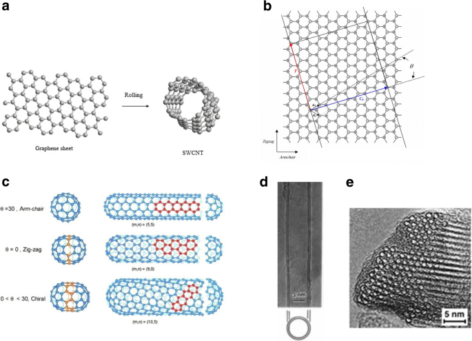
a グラファイトの単層を圧延することによるSWCNTの形成。 b 理想的なグラファイトシートからCNTを形成する図。キラルベクトル C の両端 h 重ね合わせて、1D格子ベクトル T のナノチューブを作成します とキラル角 ϴ 。 a 1 および a 2 は2Dグラファイトの基本的な格子ベクトルです(白い点は格子パイントを示します)。ジグザグとアームチェアの巻き方も示されています。 c キラリティーに基づくさまざまなタイプのCNT。 [22]から適応。 d 直径5.5nmの二重壁CNTの電子顕微鏡写真画像。 [78]から改作。 e 三角格子に詰められた〜100個のSWCNTの束の電子顕微鏡画像。 [17]
から適応CNTは非常に高い電荷キャリア移動度を持っているため、さまざまな電子デバイスアプリケーションで検討される可能性があります[24]。 SWCNTが高度な準1次元(1D)材料であり、高いキャリア移動度を備えていることを示すために、多くの進歩が見られました。 CNTのキャリア移動度の推定値は20cm 2 の範囲です。 V -1 s -1 [7]非常に大きな値(〜10 4 以上)半導体管および金属管の弾道[25]。 10 7 の電流密度 cm −2 および10 8 cm −2 SWCNTは約20μAの電流を流すことができ、SWCNTで実現可能です[26]。弾道SWCNTは、6.5〜15kΩの抵抗を示しています。 MWCNTは通常金属製で[1]、10 6 の範囲の非常に高い電流容量を備えています。 〜10 9 cm −2 [26、27]。半導体CNTのバンドギャップは、その直径に反比例することが示され(図2a)、 E で与えられます。 ギャップ =2γ 0 a C-C / d 、ここで y o C-Cタイトバインディングオーバーラップエネルギー(2.45 eV)、 a を表します C-C 最近傍C-C距離(0.142 nm)および d はチューブの直径です[28、29]。たとえば、半径0.2nmの半導体CNTのバンドギャップは約2.2eVですが、半径1.4nmのチューブのバンドギャップは約0.4eVです[30]。
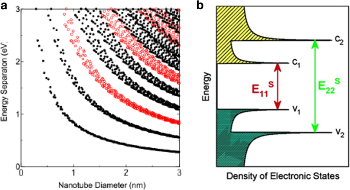
a カーボンナノチューブのバンドギャップのエネルギーとその直径に関する片浦プロット。ここで、赤い円は半導体CNTを示し、黒い円は金属CNTを示します。 [32]から適応。 b 半導体CNTの状態密度とVHSピーク(鋭い最大値で示される)を示す概略図。矢印は、光の吸収と放出のメカニズムを示しています。 [36]
から適応波動関数の境界条件は( n で変化するため、各CNTには異なる光学特性があります。 、 m )チューブのインデックスまたはキラリティー。したがって、吸収、フォトルミネッセンス、ラマン分光法などの光学特性を使用して、CNTサンプルを光子でプローブすることにより、CNTの迅速かつ非破壊的な研究を広範囲に実行できます[31、32、33]。 CNTはまた、光にさらされたときに独特の光点火特性を示し[34、35]、音波の生成とCNTの酸化をもたらします。光学分光法の結果は、各点が光学遷移エネルギー E を表すカタウラプロットによって記録できます。 ii ( i =1、2、3、...)特定の( n、m )図2aに示すように、チューブの直径の関数としてプロットされたSWCNT。 1D結晶には、エネルギーの連続関数としての状態密度(DOS)はありませんが、不連続なスパイクで上下するスパイクのようなDOSがあります。これらの鋭いスパイクまたはファンホーベ特異点(VHS)は、CNTのユニークな光学特性を生み出します[32]。 CNTの光吸収は、鋭いピークが存在するため、ほとんどのバルク材料の吸収とは異なります。 SWCNTが光を吸収すると、価電子帯のVHSの電子は、伝導帯の対応するエネルギーレベルまで上昇します。ナノチューブでは、光吸収は v からの鋭い電子遷移に関係しています。 2 c へ 2 (エネルギー E 22 )または v 1 c へ 1 ( E 11 )レベル(図2b)[36]。これらの遷移は精査され、ナノチューブの種類を特定するために使用されます[32]。
CNTの光吸収特性とは別に、通常研究されるもう1つの光学特性はそのフォトルミネッセンスです。フォトルミネッセンスは、CNTのサンプル中の半導体ナノチューブ種の量を測定するために使用されます。半導体SWCNTは、フォトルミネッセンスと呼ばれる特性である光子によって励起されると、近赤外光を放出します[37]。半導体SWCNT内の電子が励起光を吸収すると、 E 22 遷移(半導体SWCNTの価電子帯から伝導帯への電子遷移)では、電子正孔対が作成されます。 c から、電子と正孔の両方が急速に緩和します 2 c へ 1 および v から 2 v へ 1 それぞれ状態。最後に、 c を介して再結合します 1 − v 1 発光をもたらす遷移[32]。金属管では励起子発光を生成できません。電子と正孔のペアを生成できますが、金属で利用可能な多くの電子のうち、他の電子によって正孔がすぐに満たされるため、励起子は生成されません。
CNTの特性評価のための別の光学技術であるラマン分光法は、金属管と同様に半導体を検出する能力を持っており[38]、ラマン顕微鏡を介して同様に優れた空間分解能を提供できます。ラマン分光法では、光子を使用してCNTのサンプルを励起し、サンプル内のフォノンによって散乱させます。励起光子と放出光子の間の周波数の変化を分析すると、主に直径に依存する放射状呼吸モードを介して、サンプルに含まれるCNTの種類がわかります[23]。 SWCNTのラマン散乱も共鳴する可能性があります。つまり、励起レーザーエネルギーに等しいバンドギャップの1つを持つチューブのみが、吸収断面積を高めて選択的にプローブされます。
上記のCNT特性の選択された数値データを表1に示します。
<図>CNTは、その独特で望ましい特性により、これまでに多くの用途があり、いくつかの商用製品に組み込まれています。
半導体CNTは電界効果トランジスタ(FET)に使用されてきました[7、45、46、47、48](図3に回路図と I を示します。 - V 異なるゲート電圧のスイッチングを示すCNT電界効果トランジスタ(CNTFET)の特性。金属CNTは相互接続として使用されます[49、50]。単層ナノチューブと多層ナノチューブの両方が、さまざまなTHzアプリケーション(以下で説明)およびショットキーダイオード[51]でも使用されています。 CNTは現在、効率的なエネルギー貯蔵のためにリチウムイオン電池に使用されています[52、53]。水素燃料電池[54]およびCNTコーティングは、アンモニア、水素、メタンなどのガスを検知するために広く使用されています[55]。超整列カーボンナノチューブフィルムは、液晶ディスプレイ(LCD)で使用されてきました[56]。 CNTは、透明な導電性フィルムにも応用されています[57]。
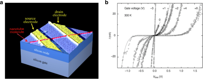
a 最初のCNTFETデモンストレーションの概略図。トランジスタは、ソース電極とドレイン電極を橋渡しするナノチューブチャネルにキャリアを誘導するゲート電圧をシリコン基板(バックゲート)に印加することによってオンにすることができます。 [45]から適応。 b 私 - V 異なるゲート電圧でのオーム挙動と非線形挙動の切り替えを示すCNTFETの特性。 [48]
から適応CNT-材料複合材料は、強化された特性を持っていることがわかっています。たとえば、CNT強化エポキシ複合材料は、純粋なエポキシマトリックスと比較して引張強度が24.8%増加することがわかりました[58]。さらに、少量の磁気的に整列したCNTを炭素繊維強化ポリマー複合材料に導入することにより、曲げ弾性率と耐荷重能力がそれぞれ46%と33%増加しました[59]。また、CNTと膨張性難燃剤を充填した熱可塑性ポリウレタン(TPU)ベースの複合材料は、優れた難燃性、迅速な自己消火性、優れた電磁干渉シールド特性、および導電性の向上を実現することが示されました[60]。さらに、CNT粉末をポリマーと混合すると、耐荷重用途の剛性、強度、および靭性が向上します[61、62]。 MWCNT-カーボンナノチューブ複合材料である磁気蛍光カーボン量子ドットは、癌治療における標的薬物輸送の担体として使用されてきました[63]。分散したCNTを含むナノ流体は、強化された熱伝達特性を示します[64]。窒素ドープCNT(N-CNT)は、食品分析の吸着剤として使用して、フルーツジュース中のビスフェノールを追跡することができます[65]。
研究者たちは、SWCNTを新しい高周波デバイスの構成要素として使用し始めています[66]。外部磁場と電場の存在下で、特定のナノチューブは強いテラヘルツ(THz)光学遷移を発生させるため、THzデバイスの調整可能な光学活性材料として有用になります。 THzアプリケーションでCNTを使用するためのいくつかの提案が開発されました。それらには、ナノチューブからの効率的な高電界電子放出を利用するナノクリストロン、大径半導体ナノチューブの負の微分伝導率に基づくデバイス、およびTHz領域で動作する単層および多層カーボンナノチューブアンテナが含まれます[66,67,68]。 。 CNTはその独自の電子特性により、テラヘルツ(THz)放射源として使用されています。現在利用可能な小型で低コストのTHz源がないため、コンパクトで信頼性の高いTHz放射源を作成することは、現代の応用物理学にとって非常に重要です[66,67,68]。 THz放射は、電磁スペクトルのマイクロ波放射と赤外線放射の間にあります。この周波数範囲では、電子輸送と光学現象が融合し、古典的な波が量子力学的光子になります。 THz範囲のこのユニークな位置は、炭素ベースのナノ材料を使用するなど、材料の電子的特性と光学的特性の間のギャップを埋める新しいアプローチによってのみ研究できることを意味します。研究者たちはまた、太陽光発電[69]や赤外線(IR)検出[70]などの分野でのCNTの使用を調査しています。
ナノスケールで合成するための反応器としてCNTを使用する可能性は、調査されている別の分野です[71]。電気触媒酸素還元反応(ORR)および酸素発生反応(OER)の触媒担体としてのCNTの使用は、広く普及しつつあります[72,73,74,75,76]。特に、さまざまな研究により、効率的なORRおよびOER反応のための窒素ドープカーボンナノ材料の使用が示され、これらのCNT電極は、白金などの金属と比較して改善された安定性と電極触媒活性を示しています[76、77]。
一般に、多数のCNTの配置、タイプ、方向、および/または構造を正確に制御することは、上記のような特定のアプリケーションのパフォーマンスを最適化するために必要です。このレビューでは、さまざまなアプローチに基づくカーボンナノチューブの組み立てと統合の進捗状況をレビューして説明します。特に、私たちは最初に、成長中の直接と成長後のアプローチの両方を介して、個々のCNTを制御するための技術に焦点を当てます。次に、得られた構造とアンサンブルとともに、多数のナノチューブを並列に統合するために開発された方法を検討します。最後に、CNTの製造と組み立てにおける過去20年間の目覚ましい進歩にもかかわらず、CNTを使用する現在のアプリケーションと新しいアプリケーションの両方に残っている重要な課題に焦点を当てます。この論文の概略図を図4に示します。
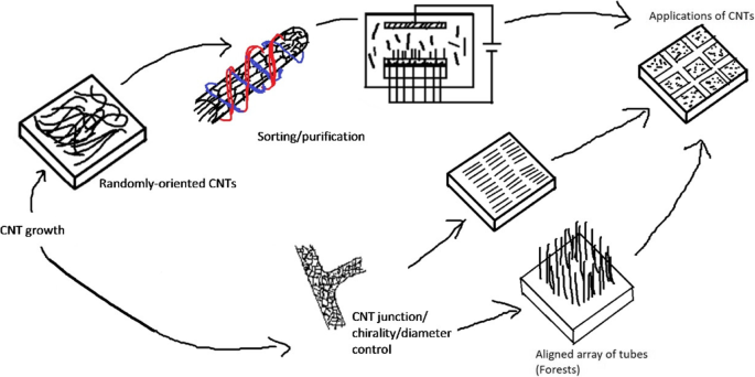
論文の概略図。このレビューでは、個々のチューブ(キラリティー、接合部、直径)からのCNTの組み立てと統合の制御から、さまざまな精製、組み立て、位置合わせ技術、および幅広いアプリケーション向けの多数のナノチューブの統合までの進捗状況について説明します
>個々のCNTの制御
CNTの成長-概要
CNTを製造するための最も広く知られている技術は、アーク放電、レーザーアブレーション、および化学蒸着である。 CNTの形成をもたらす炭素原子は、電流(アーク放電の場合)、高強度レーザー(レーザーアブレーションの場合)、および熱(CVDの場合)を利用する方法によって解放されます。これらの手法については、次のセクションで簡単に説明します。
Arc-Discharge
CNTは、アーク放電法を使用してグラファイト電極のカーボンスートから生成されました[78]。アーク放電方式では、CNTの合成に高温(1700℃以上)を採用しています。この方法は、図5に示すように大きな金属反応器に約1 mm離して配置された、アノードとカソード(直径6mmと9mm)の2つのグラファイト電極で構成されています[79]。金属反応器内で不活性ガスを一定の高圧に維持しながら、約100Aの直流電流を約18Vの電位差で印加します[80]。 2つの電極を近づけると、放電が発生してプラズマが形成されます。ナノチューブを含む炭素質堆積物が、より大きな電極上に形成されます。内径1nm〜3nmのカーボンスートの形のMWCNT。また、外径〜2 nm〜25 nmが負極に堆積していることが観察されました[1,78]。アノードにコバルト(Co)、鉄(Fe)、ニッケル(Ni)などの金属触媒をドープし、カソードとして純粋なグラファイト電極を使用することにより、SWCNTを直径約2 nm〜7nmまで成長させることができます[81 、82,83]。この手法は、大量のSW / MWCNTを成長させるために使用できます。ただし、この手法の主な欠点は、精製が必要な不要な反応後生成物を導入する金属触媒を使用しているため、収率が限られていることです。
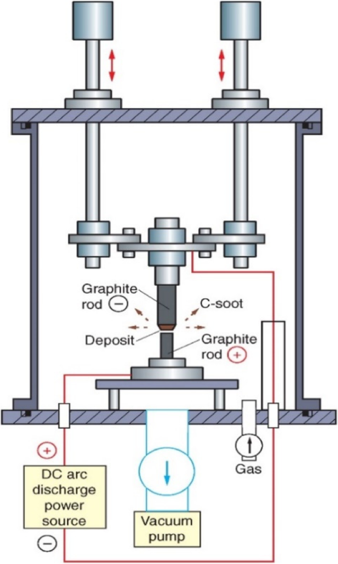
CNTの合成に使用されるアーク放電システムの概略図。この技術では、高圧と高温に維持された金属反応器内に大きなアーク電流が流れると、グラファイト電極の1つにナノチューブが生成されます。 [79]
から適応レーザーアブレーション
この手法は、アーク放電手法に似ています。ただし、アーク放電の代わりに、連続レーザービームまたは図6 [84]に示すパルスレーザーを使用します。レーザービームは、He、Ar、N 2 などの不活性ガスの存在下で、大きなグラファイトターゲットを蒸発させます。 〜1200°Cの石英管炉など。次に、気化した炭素が凝縮し、CNTが反応器のより低温の表面で自己組織化されます[85,86,87,88]。両方の電極が純粋なグラファイトでできている場合、MWCNTは内径が約1nmから2nm、外径が約10nmで生成されます[89]。グラファイトターゲットにCo、Fe、またはNiをドープすると、得られた堆積物はSWCNTの「ロープ」またはバンドルに富むことが観察されました(図1e)。生成されるCNTの収率と品質は、レーザーの特性、触媒の組成、成長温度、ガスの選択、圧力などの成長環境によって異なります。この方法は、高出力のレーザービームが必要なため、費用がかかる可能性があります。この手法の利点の1つは、不純物が少ないため、成長後の精製がアーク放電法ほど強力ではないことです。
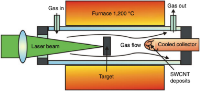
CNTの合成に使用されるレーザーアブレーションシステムの概略図。この技術では、CNTは、グラファイトターゲットを気化させるレーザービームの助けを借りて石英管炉で生成され、反応器の表面でCNTの自己組織化をもたらします。電極のタイプ(純粋なグラファイトまたはCo、Fe、またはNiがドープされたグラファイト)に基づいて、形成されたCNTは単層または多層になります。 [84]
から適応化学蒸着
化学蒸着(CVD)は、炭化水素蒸気の熱分解に金属触媒を使用するため、一般に触媒化学蒸着(c-CVD)と呼ばれます。触媒は、CNTの成長において非常に重要な役割を果たします。理想的な触媒は、基板の表面に単分散する必要があります。また、ファンデルワールス力を介して基板と適切に相互作用する必要があります。 SWCNTの成長効率は、触媒と基板の間に弱い相互作用がある場合に改善できます。高温では、金属触媒は非常に不安定であり、SWCNTのキラリティー制御された成長は困難な作業になります。理想的な触媒は、高温で優れた安定性を提供し、より良い直径分布を持つCNTの制御された成長をもたらすはずです。触媒担体と触媒ナノ粒子との間の相互作用を増加させることにより、高温で遭遇する問題のいくつかに対する制御を達成することができる。炭化水素源は、液体(ベンゼンとアルコール)、蒸気(一酸化炭素)、または固体(樟脳)の場合があります[79]。炭化水素の分解には、Fe、Co、Ni、Moなどのナノメートルサイズの遷移金属触媒が一般的に使用されます[90、91、92]。さらに、Cu、Au、Ag、Ptなどの金属触媒もいくつかの研究で使用されています[93]。場合によっては、これらの金属触媒は、SiO 2、などの触媒担体と混合されます。 MgOとAl 2 O 3 炭素原料と金属粒子が関与する触媒反応の表面積を増やすために[94]。
使用する炭化水素と触媒の種類の選択により、蒸気-液体-固体(VLS)または蒸気-固体-固体(VSS)メカニズムと呼ばれるさまざまな成長メカニズムが決まります。 2つのうち、VLSメカニズムが広く使用されています。ここで、触媒粒子は液相にあり、炭化水素が金属粒子に吸着され、触媒的に分解されます。次に、炭素は粒子に溶解することによって液体共晶を形成し、その後過飽和時に管状の形に沈殿します[95、96]。一方、VSS成長メカニズムは固体触媒を使用します[97]。
合成方法は、金属触媒の存在下、約600〜1200°Cの温度で炭化水素蒸気を分解することから始まります[98、99]。炭化水素蒸気が金属と相互作用すると、炭素と水素に分解します。水素ガスが蒸発する間、炭素は金属に溶解します。次に、触媒と基板の相互作用に基づいて、金属触媒上でのCNTの成長は、図7に示すように、先端成長メカニズムまたはベース成長メカニズム[100、101]のいずれかの形式になります。先端成長メカニズム触媒と基質の相互作用が弱いためです。ここで、炭化水素は金属の上で分解し、炭素は金属を通って拡散し始めます。 CNTは金属のベースから成長を開始し、金属の濃度勾配に基づいて炭化水素をさらに分解するための十分な余地ができるまで、より長く成長し続けます。このプロセスでは、図7aに示すように、金属が基板からさらに離れるように押し出されます。塩基成長メカニズムの場合、強力な触媒と基質の相互作用があります。先端成長メカニズムと同様に、炭化水素は金属の上部で分解し、炭素は金属全体に拡散し始めます。ただし、触媒と基板の相互作用が強いため、金属粒子は押し上げられず、図7bに示すように、CNTは金属の上に成長します。図8は、CVDによって成長したCNTの例を示しています[102、103]。
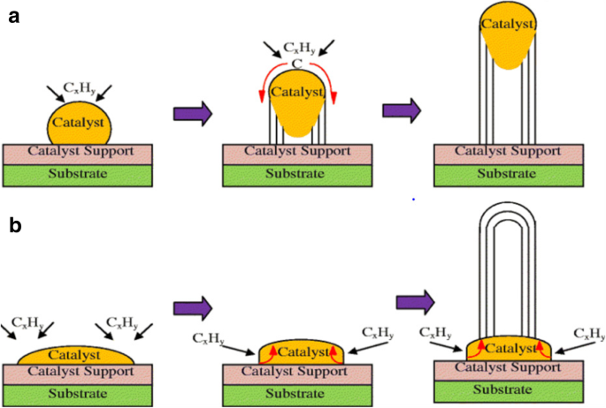
CVDを使用したCNTのさまざまな成長メカニズム([101]から採用)。触媒と基板の相互作用に基づいて、2種類のCNT成長メカニズムを見ることができます。 a 先端成長モデル:触媒と基板の相互作用が弱い場合、炭化水素が金属の上面で分解し、炭素が金属を通って下向きに拡散し、金属の底からCNTが成長する先端成長が観察されます。 b ベース成長モデル:強力な触媒と基板の相互作用により、触媒がベースに根を下ろしている間に、CNTが基板から遠く離れた金属から成長するベース成長が観察されます
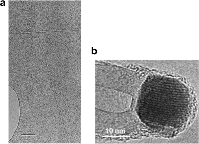
CVDを介して成長したCNTのTEM画像( a )Fe 2 を使用して成長した分離SWCNT O 3 直径5nmの触媒。スケールバーは50nmです。 [102]から改作。 b 先端に触媒粒子を用いて成長させたMWCNT。 [103]
から適応触媒のサイズと特性は、CVDを使用したSWCNTとMWCNTの成長に重要な役割を果たします。粒子サイズが小さい(数nm)とSWCNTが成長しますが、MWCNTは粒子サイズが大きい(数十nm)と形成されます[1]。炭化水素の種類は、生成されるCNTの形状に影響を与えます。たとえば、線状炭化水素であるメタン、アセチレンは、真っ直ぐな中空CNTの形成につながります。ベンゼンやフラーレンなどの環状炭化水素は、湾曲したCNTを生成します[104]。
さらに、使用する基板の選択は、触媒と基板の相互作用によりCNTの成長にも重要な役割を果たし、生成されるCNTの収率、品質、アスペクト比に影響を与えます。 CNTの成長に一般的に使用される基板のいくつかは、シリコン[104]、グラファイト[18]、アルミナ[105、106]、ゼオライト[107]などの材料でできています。研究によると、ゼオライト基板を使用すると、直径分布が狭い高収率が得られ、アルミナ製の基板は、高アスペクト比の整列したCNTを高収率で生成することが示されています[79、108]。
触媒と基板の選択に加えて、個々のCNTの構造制御も、合成手順中の温度とガス流量の影響を受けます。合成中のガス流量の制御は、使用する炭化水素のタイプ(つまり、気体、固体、または液体)によって異なります。SW/ MWCNTの直径の増加は、合成温度の上昇とともに観察されます[109]。樟脳を伴うFe-Co-zeoliteシステムでは、SWCNTの成長に理想的な温度は約900°Cであると報告されましたが、MWCNTの場合、理想的な成長温度は650°Cであると報告されました[100]。
このセクションで説明する3つのCNT製造技術のうち、CVDは、CNTの成長に対する制御性の向上、低コスト、低温の使用などのさまざまな利点により、CNTを製造するために広く使用されている技術です[79、105]。
個々のCNTの構造制御
キラリティー制御
制御可能なキラリティーを備えたCNTを成長させることは、さまざまな用途にCNTを利用するための重要なステップです。これは、CNTのキラリティーが電子バンド構造などのさまざまな特性を決定し、したがって成長するCNTのタイプ(つまり、金属と半導体)を決定するためです。キラリティー制御は、直接制御された成長または合成後の分離アプローチによって、またはこれらの方法を組み合わせることによって行うことができ[110]、CNT成長における最も困難な側面の1つと見なされています[111]。成長温度、触媒、炭化水素の種類などのさまざまなパラメータが、CNTのキラリティーに影響を与えます。直接制御成長法は、核形成プロセス中にSWCNTのキラリティーが固定されることが報告されているため、核形成プロセスを制御することによってキラリティーを制御することを目的としています[112]。たとえば、プラズマ化学気相成長法(PECVD)は、半導体SWCNTの優先的な成長に使用されてきました[113]。さらに、半導体CNTは、ST-石英基板とメタノール前駆体を使用して成長させました[114]。触媒の種類、成長温度と圧力、炭化水素の供給源などのさまざまな成長パラメータは、成長するチューブのキラリティーを制御する核形成に影響を与える上で重要な役割を果たします。シードとしてのCNT成長テンプレートの使用(金属ベースと非金属ベースの両方)、炭素分子ベースの前駆体によって開始される成長、ナノ粒子ベースの触媒の使用などの技術のいくつかは、この分野で大きな関心を集めています。これらのいくつかについて以下で説明します:
私たちが説明する最初の手法では、単一の( n 、 m )タイプのSWCNTナノチューブサンプルは、より小さな断片(シード)に切断されます。各ピースは、VLS増幅プロセスを使用してより長いナノチューブを成長させるためのテンプレートとして使用することを目的としています(図9a)。この方法の主な目的は、大量の n を成長させることでした。 、 m -制御された構造。各シードは、ポリマーで包まれたSWCNTであり、末端がカルボキシル化され、末端がFe塩でつながれていました。成長プロセスの間、Fe塩は成長触媒として機能し、狭い直径分布を達成することを目的としたVLSメカニズムの使用[115]。この方法で成長したSWCNTは、成長シードの直径と同様の直径を持っていました(図9b–f)。しかし、成長したチューブのキラリティーの変化に関する詳細は明確に確立できませんでした[116]。さらに、この方法では、成長したSWCNTに金属粒子が存在するため、複雑な精製ステップが必要になり、最終製品の品質に影響を及ぼします。
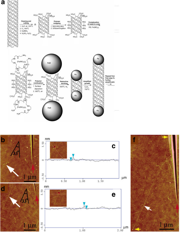
a 成長テンプレートとしてFeシードを使用したSWCNTの成長メカニズム。 [116]から改作。 b 、 c 増幅プロセス前のSWCNTの原子間力顕微鏡(AFM)画像と高さ分析。 [116]および d から適応 、 f 増幅成長プロセス後。 [116]から改作。白い矢印は元のSWCNTシードの位置を表し、赤い矢印はロケーターの刻印に対するシードの位置と角度を示し、黄色の矢印は増幅されたナノチューブの全長を示します。 [116]
から適応金属触媒ベースの成長の代替として、別の技術は、成長テンプレートとしてSiやGeのような半導体ナノ粒子を使用することによってCNTの制御された成長を含みました。これらの実験の1つでは、850°Cでエタノールから熱分解された炭素原子を導入することにより、半導体ナノ粒子(サイズ5 nm以下)を使用してCNTを成長させました。しかし、この実験で成長したCNTは、触媒としてFe、Co、またはNiを使用した実験と比較して、非常に低品質で低収率であると見なされました[117]。別の成長技術は、一般に「クローニング」と呼ばれるオープンエンドの成長メカニズムによるものでした(図10)[118]。ここで、SWCNTのキラリティーは、別の金属触媒を使用せずに、シード/触媒としてオープンエンドSWCNTを使用することによって制御されました。これらのシードを使用して、複製CNTをSiO 2 上で成長させました。 / Si基板。この方法で報告された総収率は約9%でしたが、石英基板上でこの方法を使用してSWCNTを成長させることにより、40%に改善することができました[118]。気相エピタキシーに基づく別の技術を使用して、事前定義されたキラリティーでSWCNTを成長させました。この方法では、デオキシリボ核酸(DNA)で分離された単一キラリティーSWCNTシードを成長テンプレートとして使用することにより、CVDとSWCNTの分離技術を組み合わせました。これらのシードは非常に高純度(〜90%)でC 2 H 5 OHおよびCH 4 炭素源として使用されました。この実験は、数百nmから数十ミクロンに成長したSWCNTの有意な伸長を示しました。この方法で生成される総収率は非常に低く[110]、気相エピタキシー(VPE)ベースの成長技術に関連するいくつかの研究は、収率を向上させることを目的として進行中です。
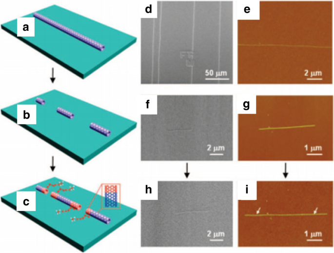
a – c 「クローニング」メカニズムを介してテンプレートとして電子ビームリソグラフィーカットナノチューブセグメントを使用した超長SWCNTの成長プロセスを示す概略図。 [118]から改作。 d 、 e SEMおよびAFMは、オープンエンドSWCNTシードの準備に使用されるSWCNTを画像化します。 [118]から改作。 f 、 g 2番目の成長のための短い親SWCNTセグメントのSEMおよびAFM画像[118]から適応。 h 、 i 重複したSWCNTのSEMおよびAFM画像は、SWCNTから成長し続けました。 [118]
から適応キラルSWCNTを選択的に成長させる1つの方法は、シリカ基板とCo-Mo触媒を使用することです[119]。この手法では、(6,5)および(7,5)キラリティーのナノチューブが得られました。 Co酸化物とMo酸化物の間の適切な相互作用により、高温でのCoナノ粒子の凝集を回避できます。さらに、ガス状の供給組成、成長、および温度を最適化することにより、(6,5)ナノチューブの選択性が約55%向上しました[120]。 (6,5)SWCNTの選択的成長のための別のアプローチは、Co-Si触媒を使用して実証され、狭い分布のキラルSWCNTを提供しました[121]。高品質(6,5)チューブも、触媒組成を調整することにより、キラリティー分布が狭いシリカ-二金属CoPt触媒上で大気圧アルコールCVDを使用して800°Cで成長しました[122]。 (9,8)SWCNTは、Coナノ粒子とナノポーラスSi担体(TUD-1)を使用して高い選択性で成長しました[123]。最近、(12,6)SWCNTは、タングステンベースのバイメタル固体合金触媒W 6 を使用して合成されました。 Co 7 、純度> 92%(図11)[124]。この高レベルの純度は、W 6 に起因していました。 Co 7 2400°Cという非常に高い融点を持ち、ナノ粒子触媒を使用することで高純度SWCNTを成長させるための潜在的な手段を提供する触媒。
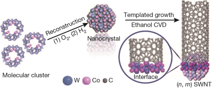
タングステンベースのバイメタル固体合金触媒(W 6 )を使用した高純度の単一キラリティー(12,6)SWCNTの成長 Co 7 )。これらの合金ナノ粒子は、SiO 2 上でのCNT成長を触媒します。 CNT成長中のキラリティー制御に役立つエタノールCVDによる/ Si基板。 [124]
から適応最近、「触媒コンディショニングプロセス」として知られる技術を使用した触媒の失活プロセスに基づいて、直径が0.8〜1.2nmの範囲の半導体SWCNTの選択的成長が報告されました[125]。ここで、金属SWCNTの成長を促進する触媒は、触媒調整パラメーター(酸化的、つまり水)と還元的(つまりH 2 )にさらされます。 )これらの触媒の失活につながる成長プロセスの前のガス。この研究では、触媒の失活に基づく収率と選択性の逆の関係が報告されました。
有機化学の分野で進化する方法論により、キラリティーが制御されたCNTの成長に使用できるさまざまな炭素ベースの前駆体の合成が可能になりました。いくつかの例には、フラットCNTエンドキャップ、3次元CNTエンドキャップ、カーボンナノリングが含まれます[111、126、127]。これらはすべてテストされ、制御された環境下でCNTの成長を刺激することが証明されています。ただし、これらの各アプローチにはいくつかの制限があります[128]。
ある方法では、半球形のキャップを生成するために、熱酸化を使用してフラーニオンを開きました。しかし、形成された半球冠構造の制御が欠如しているため、単一キラリティーCNTの合成には課題がありました[129]。キャップのない側壁セグメントと見なされるカーボンナノリングを使用したCNTの合成も開発されましたが[126]、研究者は成長したままのCNTのキラリティーを制御できませんでした。別の手法は、有機化学アプローチを使用してC 50 の純粋な分子シードを合成する他の研究者によって開発されました。 H 10 (5,5)キラリティーナノチューブのエンドキャップとして[130]。この方法では、研究者らは、金属を含まないVPE伸長によるSWCNTのキラリティー制御合成を実証しました(図12a)。成長したナノチューブはよく整列していて高密度であるにもかかわらず、ラマン特性評価では、合成されたSWCNTは(5,5)キラリティーではないことが観察されました。成長したままの半導体ナノチューブはより小さな直径であることが観察された[130]。ほぼ同時に、エンドキャップ前駆体と平面単結晶金属表面を使用して、所定のキラリティーを持つ単一キラリティーSWCNTを合成する別の方法が実証されました[131]。この方法では、研究者のカスタムが前駆体(C 96 、H 54 )有機化学アプローチを使用して、表面触媒による環化脱水素プロセスにより(6,6)ナノチューブシードを生成します(図12b)。 532 nmレーザーを使用したラマン特性評価では、合成されたSWCNTが(6,6)キラリティーを持っていることが確認されましたが、532 nmは(6,6)ナノチューブと共鳴していないと主張する研究者もいます。彼らの研究では、532 nmが(9,2)または(10,0)キラリティーナノチューブと共鳴していると引用しました。さらに、Gバンドの分割が、アームチェアの金属ナノチューブのGバンドを単一の対称ピークとして示したこの分野の初期の研究と一致しないことを観察した人はほとんどいません[132、133]。研究者らは、成長したままのSWCNTが(6,6)キラリティーであるかどうかを判断するために、さらにラマン特性評価、STM研究を推奨しています。有機化学技術の使用は、より高純度の大規模合成の可能性があるため、キラリティー制御されたSWCNT合成のさらなる開発で参照される可能性があります。
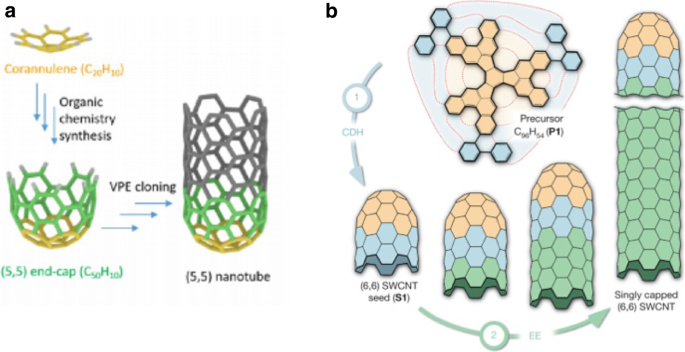
a 金属を含まないVPE伸長による(5,5)SWCNTのキラリティー制御合成に使用される構造分子エンドキャップ。 [130]から改作。 b 分子エンドキャップ前駆体からのSWCNTの2段階ボトムアップ合成の概略図。単一にキャップされた超短(6,6)シードは、炭素供給原料ガスの表面触媒分解に由来する炭素原子を使用して、ナノチューブのエピタキシャル伸長をもたらします。 [110]
から適応SWCNTの成長に使用される製造方法のほとんどは、金属、半金属、および半導体の特性を持つ多分散CNTを生成します。このバリエーションは、グラフェンシートの巻き方に基づいており、インデックス( n、m )で示されます。 )成長したチューブのキラリティーを定義します。複数の導電率タイプが存在するとデバイスの性能が低下する可能性があるため、これらの変動を制御する手順は、SWCNTのさまざまなアプリケーションにとって不可欠です。初期の技術のいくつかは、メタンプラズマ[134]、水蒸気[135]、酸素[136、129、137]、水素[134]のような気相エッチャントの使用を含み、これは合成中に金属粒子をエッチングするためです。金属ナノチューブとの反応性が高いため、半導体ナノチューブが残ります。
m-SWCNTの選択的除去において、エッチャントとして酸素を使用する浮遊触媒化学蒸着(FCCVD)技術を使用すると、直径1.4〜1.8 nmのs-SWCNTを含む約90%の収率が得られました[137]。ただし、酸素は、成長プロセス中の強力な酸化特性により、他の炭素ベースの材料と結合する可能性があります。成長過程で酸素濃度を制御することは困難な作業です。別の方法として、水蒸気は酸化能力がはるかに弱いため、CVD技術のエッチャントとして使用できます。この手法では、約97%の収率が報告されています[138]。
最近の研究では、エッチングメカニズムに対する直径依存性の重要性が報告されています。研究の1つでは、メタンプラズマを使用してm-SWCNTを選択的にエッチングし、続いてアニーリングしました。最後に、s-SWCNTは高温で安定した成長基板上に保持されます[139]。直径分布をSWCNT直径の最適範囲に狭めることにより、ほとんどのm-SWCNTはこの範囲内でエッチングされます。別の手法では、直径分布を制御するために、Fe–W(鉄-タングステン)ナノクラスターなどの二金属固体合金触媒を触媒前駆体として使用しました。これは、タングステンの高温安定性により、CVD合成中にナノクラスターが安定するためです。成長プロセス中、水蒸気がエッチャントとして使用されました。図13に示すように、この手法では約95%の収率が報告され、石英基板上に形成されたs-SWCNTの約90%の直径は2〜3.4nmの範囲であると報告されました[140]。触媒としてFeナノ粒子を使用した同様の実験が行われ、Feナノ粒子の移動性により、全体の収率が触媒粒子サイズの広い分布を示しました。これは通常、高温CVD成長中に液体状態になります[94]。
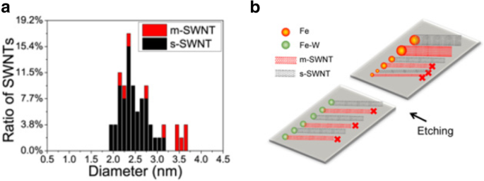
a 522ppmの水蒸気濃度下でのFeW触媒SWCNTの直径とキラリティー分布。調製されたままのSWCNTの約90%は、[140]から採用された2.0〜3.2nmの直径範囲にあると報告されました。 b 成長中の直径依存および電子タイプ依存のエッチングメカニズムの概略図。 s-SWNTの高い選択性は、Fe-W触媒を介して直径を制御することによって得ることができます。 [140]
から適応直径分布の狭いs-SWCNTを成長させる別の手法は、図14に示すように、炭素でコーティングされたコバルトナノ粒子触媒(ドングリ様触媒と呼ばれる)を使用することです。Coナノ粒子は、SWCNT成長の活性触媒相として機能します。外側の端のカーボンコーティングは、Coナノ粒子の凝集を防ぎます。これは、高温でのSWCNTの成長中に大きな粒子の形成につながるほとんどの成長方法が直面する主要な問題です[141]。この手法では、成長したs-SWCNTの収率は約95%で、直径分布は1.7nmを中心に非常に狭くなっています[138]。
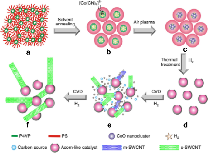
カーボンコーティングされたCoナノ粒子触媒を使用した、直径分布の狭いs-SWCNTの成長の段階的な説明。溶媒アニーリング、空気プラズマの使用、それに続く熱処理により、直径が約1.7 nmのs-SWCNTが約95%の収率で得られました。 a ポリ-(スチレン-ブロック-4-ビニルピリジン)フィルムは、垂直ナノシリンダーに自己組織化されます。 b 垂直ナノシリンダーからの相分離ナノドメインの形成とそれらへのK3 [Co(CN)6] 3触媒の吸着。 c ポリマー層に部分的に囲まれたCoOナノクラスター。 d どんぐりのような二成分触媒を生成するために部分的に炭素でコーティングされたCo触媒ナノ粒子。 e 部分的に炭素でコーティングされたCoナノ粒子からの狭い直径分布を持つSWCNTの成長と、それに続くm-SWCNTのその場エッチング。 f s-バンドギャップ分布が狭いSWCNT。 [138]
から適応CNTジオメトリの制御
直径
制御可能な直径を持つSWCNTの成長は、その電気的、表面機能化、および熱的特性に影響を与える重要なパラメーターの1つと見なされています[1]。バンドギャップやキラリティーなどの特性は、形成されるSWCNTの直径の変化によって制御できます。 SWCNTの直径制御は、フローティング触媒法を使用した成長、または触媒を上に堆積させた基板成長法、またはテンプレート成長アプローチを使用した成長による場合があります。最初の2つの手法のうち、浮遊触媒法による成長は、触媒が基板の単一平面に制限されないため、凝集が制限されるために成長するチューブの直径をより適切に制御できます。研究によると、この方法を使用すると、直径が約1.2〜2.1nmの範囲で制御されることが示されています[126]。研究の1つでは、直径の制御はCO 2 を追加することによって達成されました (これは、小さな直径のチューブをエッチングするためのエッチング剤として機能します)エアロゾルCVD反応器への炭素源を使用します。対応する透過型電子顕微鏡(TEM)画像と、異なるCO 2 で成長したSWCNTの吸収対波長プロット 濃度は下の図15に示されています。 CO 2 の濃度を上げる 図15cに示すように、SWCNTの直径が1.2nmから1.9nmにシフトします[142]。触媒のサイズと特性も、SWCNTとMWCNTの成長を制御する上で重要な役割を果たします。粒子サイズが小さい(数nm)とSWCNTが成長しますが、MWCNTは粒子サイズが大きい(数十nm)と形成されます[143]。たとえば、平均直径9および13 nmのFe触媒を使用すると、平均直径7および12nmのMWCNTが生成されました[105]。
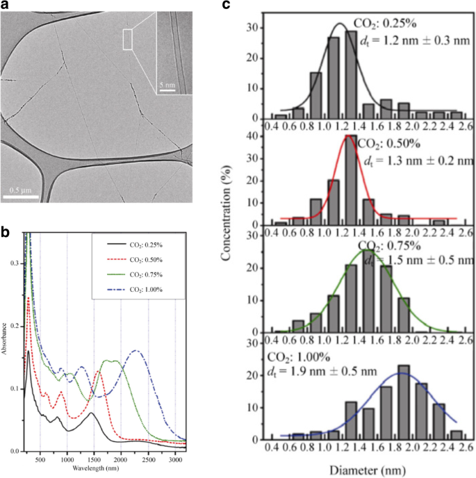
a CO 2 を添加して成長させたSWCNTのTEM画像 炭素源と一緒に。 (挿入図)は、[142]から採用された個々のSWCNTのTEM画像を示しています。 b 異なるCO 2 で成長したSWCNTの吸収と波長を示すプロット 濃度。 [142]から改作。 c 異なるCO 2 のSWCNTサンプルの対応する直径分布 濃度。 [142]
から適応基板成長法は、触媒間隔を広げることによって粒子の凝集を最小限に抑えることを目的としています。たとえば、フェリチン触媒粒子を使用してCVDを介して堆積する前にナノ粒子を遠心分離すると、の範囲で直径が制御されます。 1.9〜2.4 nm [144]。または、Al 2 の間にFeを挟みます O 3 サンドイッチ触媒モデルでは、直径が0.8〜1.4nmのSWCNTが合成されました[145]。ただし、これらの手法を使用して成長したSWCNTは、触媒間隔が大きいために絡み合っていました。
SWCNTの直径を制御する別の方法は、テンプレートベースの成長アプローチを使用することです[126、146、147、148]。成長テンプレートとしてアームチェアCNT(図16)の最短側壁セグメントを表すカーボンナノリング(シクロパラフェニレン)を使用し、炭化水素源としてエタノールを使用して、直径が1.2〜2.2nmの範囲のSWCNTを成長させました。さまざまなタイプのナノリング(構造内のベンゼン環の数に基づく)が成長テンプレートとして使用されました。成長したSWCNTの直径は、使用されたカーボンナノリングの直径と同様であり、それにより、有機化学アプローチを使用したSWCNTの直径制御の手段を提供しました。
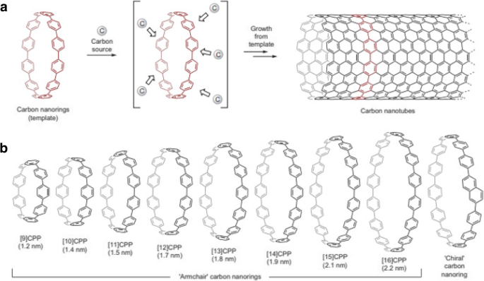
a アームチェアCNTの最短側壁セグメントを表すカーボンナノリング(シクロパラフェニレン)を使用したテンプレートベースのCNT成長の概略図。 [126]から改作。 b テンプレートベースの方法を使用して成長したさまざまなカーボンナノリングとそれに対応する直径(nm)の表現。 [126]
から適応いくつかの方法は、制御された直径を持つMWCNTの成長を報告しています[149,150,151,152,153,154]。方法の1つでは、直径が20〜400 nm、長さが0.1〜50μmの整列したCNTを、プラズマ化学気相成長法を使用して触媒サイズを調整することにより生成しました(図17a)。別の方法では、大径ナノチューブの形成における炭素反応物の供給と成長温度の重要性が報告されています[105]。ここでは、直径9 nmの鉄ナノクラスター、炭素反応物としてのエチレン、900°Cの成長温度を使用して、2つまたは3つの壁を持つ大径のナノチューブを製造しました。あるいは、リソグラフィーでパターン化された金属ナノクラスターを使用して、直径が約1.5 nmのSWCNTのアレイを取得しました(図17b)。
異なる直径のナノ粒子触媒を使用して生成されたCNTのCVDベースの成長。 a ニッケルコーティングされたガラス基板を使用して、さまざまな直径(直径250nmと20nm)で生成されたCNTのSEM画像。 [149]から改作。 b リソグラフィーでパターン化された触媒と直径〜1.7nmのCoナノ粒子を使用して成長させたナノチューブのAFM画像。 [150]
から適応ジャンクション
接合部のような形成につながるCNTの成長の変化は、新しい電子スイッチングデバイスやトランジスタに使用できる3端子Y接合のようなナノチューブ構造を作成することができます[155、156、157、158]。 Y接合ナノチューブは、図18aに示すように、調整可能なステムおよびブランチテンプレート[159、160]を備えた陽極酸化アルミナテンプレートを使用してCVDによって成長させることができます。別の方法では、成長プロセスでTiドープFe触媒を使用して、石英基板上にY字型接合の形で分岐したMWCNT(〜90%)を生成しました(図18b)[161]。
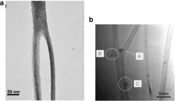
a 分岐ナノチャネル陽極酸化アルミナテンプレートを使用してCVDによって成長させたMWCNTY接合ナノチューブのTEM画像。成長したY接合は、長さが6〜10μmで、直径が調整可能であると報告されています。 [159]から改作。 b TiドープFe触媒を使用して成長させたMWCNTY接合ナノチューブのTEM画像。接合部に存在する触媒(Aとして示されている)は、2つの分岐の形成につながります。 Bは、ナノチューブの壁に付着する触媒粒子から成長したY接合を示しています。 Cは、それ以上の分岐を引き起こさない触媒ナノ粒子を表します。 [161]
から適応上記の技術に加えて、走査型電子顕微鏡(SEM)を使用して、接合部に電子ビームを照射することによって接続された異なるCNTの交差によって形成されたSWCNT接合部も報告されています[162、163]。ここで、電子ビームの影響下で、成長プロセスで使用される炭化水素はアモルファスカーボンに変換され、次にナノチューブを付着させて機械的接合を形成するために利用されます(図19a、b)。別の同様の研究では、さまざまなカーボンナノチューブ接合部(Y字型、T字型)が電子ビーム溶接によって形成され、ナノチューブに構造的欠陥が生じ、ダングリングボンドの架橋によるチューブの接合につながりました(図19c、d )[162]。
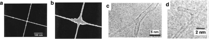
MWCNTナノチューブ接合部の成長( a )前と( b )電子ビーム照射によるアモルファスカーボンの堆積によるはんだ付け後。 [163]から改作。 c 電子ビーム照射により形成されたY字型の接合部。 [162]から改作。 d 予め形成されたY接合を照射した後に形成されたT字型ナノチューブ接合。 [162]
から適応あるいは、2端子SWCNT接合は、CVDプロセス中に温度変調を使用して制御された方法で成長させることができます(図20)[141]。この方法では、成長温度を変えることにより、SWCNTの直径とキラリティーの系統的な変化がSWCNTの分子内接合の形成につながります。これらの接合部は、CVD中に赤外光を使用して基板の温度を局所的に上昇させることにより、所望の位置で成長させた。また、温度を上げると成長する接合部の直径が小さくなり、その逆もあり、成長する先端に存在する触媒粒子は変化しませんでした[141]。
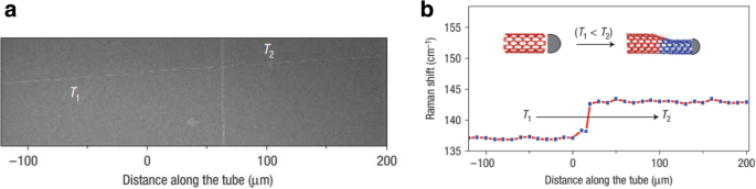
a CVD成長中の温度を950から900°Cまで変化させることによって形成された2末端SWCNT分子内接合のSEM画像(温度はT 1 で示されます およびT 2 )。 [141]から改作。 b 温度の変化に伴うラマンスペクトルの対応するシフト。挿入図は、温度によるSWNTの直径変化の概略図を示しています。 [141]
から適応成長後のシングルチューブの精製/選別
FETやナノスケールセンサーなどの高度なアプリケーションの多くは、構造変化がほとんどない単分散サンプルを必要とするため、CNTソーティング方法を理解することは重要です[164]。 CNTの選別を行う前に、チューブを液体媒体(水または有機溶媒)に分散させる必要があります。 Unfortunately, there are certain constraints which may prevent separation in an aqueous dispersion. For example, CNTs have very strong Van der Waals interactions which restrict sorting [87]. There are several well-developed techniques currently being used for the post-growth purification or sorting of tubes. Some of these are discussed below.
One of the techniques, commonly referred to as the density gradient ultracentrifugation (DGU), has been shown to produce a high yield of pure SWCNTs, without much need for chemical treatment of the sample [165, 166]. DGU, which depends entirely on the buoyant density of the CNT, is an isopycnic separation process. The process is achieved by wrapping the SWCNT sample with a surfactant (Fig. 21) [166]. After the grown SWCNTs are mixed with the surfactant, the aqueous dispersion of surfactant-encapsulated tubes is added to the centrifuge tubes, which contains a pre-existing density gradient medium. A strong centrifugal force is then applied, and it causes the surfactant-wrapped SWCNTs to be separated by the movement of SWCNTs to regions of the density gradient medium which match the tubes’ buoyant densities (isopycnic points). The aqueous dispersions of the SWCNTs are produced by using either linear chain surfactants or bile salts. The density gradient medium is usually made of a salt (lithium chloride, cesium chloride, sodium chloride) solution in water. Nonlinear gradients are preferred because they are very sensitive and allow trapping of particles over the entire length of the centrifugal cell. The gradient density and its variation are important to the sorting process wherein, the gradient needs to be set up such that the distance between the tubes and their isopycnic points is minimal. As the density gradient medium responds to the centrifugal force, it leads to steeper gradient over time and hence redistribution of the density profile takes place during centrifugation [167]. After the centrifugation process, the sorted SWCNTS are removed layer by layer using the fractionation process (using piston, upward and downward fractionation methods), which involves extracting quantities of mixtures to different aliquots which vary in composition with respect to the density gradient of the original mixture. Uniform surfactant coverage is important or adsorbed surfactant molecules will begin to aggregate and form clusters along the tube sidewalls, thereby impeding effecting separation of the tubes. To separate metallic and semiconducting tubes, a co-surfactants mixture is used for the ultracentrifugation process. After the semiconducting tubes have been separated, chirality enrichment of tubes is carried out to generate samples that are rich in a certain chirality of tubes, and the resulting semiconducting-SWCNTs-enriched fraction is passed through a dialysis membrane to remove the surfactants from the SWCNT sidewalls [168]. Finally, the tubes are characterized using various optical spectroscopy methods.

a Illustration of DGU separation of tubes coated with surfactant based on their diameter and metallicity. The near infrared absorption spectra of SWCNTs is also shown. Adapted from [166]. b Clear separation of SWCNTs by electronic type and the corresponding absorbance spectra for semiconducting SWCNTs (in red) and metallic SWCNTs (in blue) is shown. Adapted from [166]
Another separation technique, referred to as the ion-exchange chromatography (IEX), is based on the ion-exchange processes occurring between a mobile phase and stationary ion-exchange groups (which are bonded to the support material). The IEX separation method is carried out on single-stranded-DNA-wrapped (ssDNA) SWCNTs, which have different electrostatic interactions with an ion exchange column [169, 170]. By selecting the desired sequence from the vast ssDNA library, purification of the specific (n, m) species was possible. With certain ssDNA sequences greatly improving separations between metallic and semiconducting CNTs as well as between semiconducting CNTs of different diameters and electronic band gaps [171]. The IEX process begins by wrapping ssDNA around individual SWCNTs, to form DNA/CNT hybrids. Some of the DNA/CNT hybrids in aqueous dispersions are electrostatically bound to the positively charged anion-exchange resin (stationary phase). As the mobile phase is passed over the hybrid-resin system, and its ionic strength increases, hybrids with the lowest effective charge density elute within the shortest IEX times. Because the hybrids are found in both the stationary and mobile phases, the separation is based on differences in this distribution. There is less electrostatic attraction between metallic hybrids and the IEX resin than between semiconducting hybrids and the IEX resin, thus in a mixture of metallic and semiconducting CNTs of the same diameter, the metallic hybrid will elute from the column first. This method of DNA-wrapped CNTs produced many single-chirality semiconducting CNTs. Figure 22a shows the optical absorption spectra of 12 purified semiconducting SWCNTs along with their structure. This method could also be used for purification of armchair metallic tubes [133, 169]. An alternative approach to sort metallic and semiconducting CNTs is using anion-exchange chromatography technique. Here, single-stranded DNA form stable complexes with CNTs and can effectively disperse them in water. Here, the chosen DNA sequence self-assembles into an ordered structure around an individual nanotube, helping in nanotube formation (Fig. 22b).

Purification of CNTs with defined helicity with the aid of specific DNA sequences using IEX. a Absorption spectra of twelve purified semiconducting CNT species along with their (n, m ) structural notations. Adapted from [169]. b Molecular dynamics model of (8,4) nanotube obtained by rolling a 2D DNA sheet with ATTTATTTATTT strands. Orange color indicates thymine, green color indicates adenine and yellow color shows the backbones. Adapted from [169]. c 、 d Chirality separation of SWCNTs using allyl-dextran-based multi-column chromatography. c Using SDS as a single surfactant, the dispersed SWCNTs were adsorbed on column medium and, upon saturation, the single-chirality tubes are enriched according to its binding affinity towards the column. Adapted from [176]. d Bulk separation of iterative column chromatography to produce single chirality enriched SWCNTs, showing their distinct colors according to their chirality. Adapted from [176]
Gel chromatography, particularly, agarose gel chromatography is a method of separating semiconducting CNTs from metallic CNTs in an mass-spectroscopy mixture using hydrogels [172, 173]. Agarose gel beads are used for mass-spectroscopy separation, owing to their simplicity, affordability, short process time of about 20 min and scalability. The mechanism for gel chromatography follows a few simple steps. First, the SWCNT mixture, containing both metallic and semiconducting CNTs, would be dispersed in an aqueous surfactant solution, such as sodium dodecyl sulfate (SDS). The wrapping and encapsulation of the SDS surfactant molecules around SWCNTs plays a crucial role in the separation mechanism. The interaction between SDS molecules and SWCNTs via ion-dipole forces depends on the pH condition and concentration of SDS molecules. Due to the electrostatic properties of SWCNTs [174], SDS molecules form different types of micellar structures around semiconducting and metallic SWCNTs [172, 175]. On semiconducting CNTs, randomly oriented, flat micellar structures are formed, while for the metallic CNTs, cylindrical micellar structures are formed. This is mainly due to difference in ion-dipole forces between metallic and semiconducting CNTs during their adsorption on agarose gel. These disparate encapsulation mechanisms form the basis of the separation process. After the SWCNT dispersions are formed, they are ultra-centrifuged to remove SWCNT bundles and other impurities, and the SWCNT-surfactant solution is pipetted to be used in the separation process. Next, a separating column is filled with agarose micro-beads suspended in ethanol, after which the column is washed and equilibrated using the surfactant aqueous solution. The agarose-SWCNTs mixture, which is to be separated, is then poured into the column, and the SDS solution is added. This causes a displacement of the SWCNT dispersion along the column. A portion of the SWCNTs (the semiconducting CNTs) are trapped at the top layer of the agarose beads, while the metallic CNTs move to the bottom of column. This movement is related to the encapsulation of the tubes. Because semiconducting SWCNTs are encapsulated by flat randomly oriented SDS micelles, and have less surfactant coverage, there will be an ineffective shielding between the semiconducting SWCNTs and the agarose gel, and thus, a stronger affinity of the semiconducting SWCNTs to the gel. However, the metallic SWCNT walls are surrounded by an ordered high-density cylindrical micellar structure, which causes a steric hindrance between the SWCNTs and the agarose gel. Therefore, the metallic tubes have less affinity to the agarose gel. A schematic of SWCNTs separation based on the chirality of the tubes is shown in Fig. 22c, d [176].
Another technique to separate metal and semiconductor nanotubes is using the technique of dielectrophoresis (DEP). When a particle is placed in an electric field, a lateral force, also known as a dielectric force acts on it [177]. This force can be used to manipulate nanoparticles or cause them to move, and the resulting movement of particles is termed dielectrophoresis [178]. The operating principle of the alternating current (AC) DEP process is based on the fact that metallic and semiconducting CNTs have different dielectric constants. The setup consists of a fabricated microelectrode, fluidic chamber and the SWCNT solution. The DEP force is generated by applying a non-uniform electric field to the setup. Due to the applied electric field, a dipole moment is induced on the SWCNT mixture, and the tubes will move towards the maxima or minima of the electric field depending on their polarity. Under the action of an AC electric field, CNTs in solution will move to the electrodes depending on their surface charge [179,180,181]. The electrodes are typically fabricated using e-beam lithography, which are then attached to a function generator. When an AC electric field originating from the function generator operating at 20 V peak-to-peak voltage and a frequency of 10 MHz is applied, a suspension of ~ 10 μL of SWCNTs is deposited. The metallic nanotubes will attach themselves to the electrodes, while the semiconducting tubes will remain in the suspension (Fig. 23) [182]. This is due to the divergent responses of the different types of CNTs to the electric field. In this technique, direct current (DC) electric field is not usually used as it leads to aggregation of CNTs near one of the electrodes [179]. The applied electric field and deposition time are the crucial parameters which control the CNT deposition yield.

a Schematic of the experimental setup of the dielectrophoresis of a SWCNT solution using a microelectrode array. The metallic tubes (in black) are deposited on the electrodes and semiconducting tubes are left in suspension (in white). Adapted from [182]. b Rayleigh scattered dark-field micrograph showing aligned SWCNTs (in green) and the corresponding polarized SWCNTs perpendicular to the electrodes. Adapted from [182]
Gel electrophoresis was developed as an improvement to the AC dielectrophoresis method. This process makes use of the same mechanism as AC electrophoresis but uses agarose gel as a medium. SWCNTs dispersed in an aqueous SDS surfactant are used to fill a gel column and subjected to an electric field. This causes a movement of the m-SWCNTs through the gel medium to the anode while the s-SWCNTs are adsorbed to the gel [177, 178].
Sorting of CNTs can also be done using solution-based conjugated polymers which can be used for selecting pure semiconducting SWCNTs from CNT samples. Here, semiconducting CNTs are wrapped with conjugated polymers, and this technique is considered helpful for selective and large-scale sorting of CNTs [183]. In this method, the SWCNT-polymer mixture is sonicated in an organic solvent for half an hour in order to disperse the SWCNTs. Next, the polymer-wrapped SWCNT solution is centrifuged for about an hour, which results in the sedimentation of m-SWCNTs. Finally, the s-SWCNT supernatant/liquid, which is found lying above the m-SWCNT sediments, is collected for use [183].
In another technique, a gas-phase plasma hydro carbonation reaction is used to selectively etch and gasify metallic nanotubes, retaining the semiconducting nanotubes in near-pristine form [139]. In this method, an array of 98 devices each consisting of ~ 0–3 as-grown SWCNTs grown using CVD were fabricated on an oxide-coated Si substrate. Each SWCNT was of ~ 1–2.8 nm in diameter. These arrays consisted of 55% semiconducting tubes which were non-depletable by the sweeping gate voltage, and about 45% metallic tubes which were depletable with on/off conductance ratio of ≥ 10 3 。 These arrays were exposed to methane plasma at 400 °C and then annealed at 600 °C in a quartz tube furnace. Post this, it was observed that the metallic CNTs were selectively removed and the semiconducting tubes were left behind in a greater proportion of about 93%.
Assembly/Placement/Integration of Multiple CNTs
Integrating multiple CNTs is essential for the realization of large-scale device applications. This has proved challenging due to the need for precise control and positioning of the fabricated CNTs with respect to other device elements. In this section, we focus on some of the existing techniques that are used in the process of batch level control, fabrication of multiple CNTs and their subsequent integration onto the substrates.
Batch Level Control
Catalyst Patterning
During CVD, a catalyst is often dispersed on the substrate from a solution containing a suspension of the nanoparticles. This is done by spin coating the substrate or by dipping the substrate into the catalyst solution. Alternatively, catalysts can also be deposited on the substrates by evaporation to create thin films. In order to position the catalysts at specific locations, different lithographic techniques like photolithography and microprinting have been reported.
Photolithography is used to pattern the catalyst which leads to growth of CNT thin films after lift-off. In one of the methods, controlled growth of CNTs with diameters of 0.5–1.5 nm was reported using Fe salt as catalyst. In this work, photolithography produced liquid catalyst islands on polymethyl methacrylate (PMMA) and alumina substrates. However, most of the CNTs grown were randomly oriented [184, 185]. Self-assembled masks can also be used to pattern catalysts in solution in order to control the positioning and alignment of nanotubes [186]. Another work reported the controlled growth of CNT thin films in certain regions by catalyst particle patterning using self-assembled monolayers. Here, a thick silicon substrate was thermally oxidized and positive photoresist mesas where CNT thin films were formed were patterned [187]. In a recent work, the growth of SWCNTs with diameters in the range of 0.7 nm to 2.6 nm using Prussian blue analog (PBA)-based bimetallic catalysts was reported [188]. Control on the overall catalyst size and properties was possible by synthesising PBA nanoparticles with narrow size distribution. Silicon wafers coated with an oxide layer were used as substrates. On these, a self-assembled monolayer of silane molecules (having a pyridine group at the ends) was deposited in order for the bond formation with the PBA nanoparticles to occur. Catalyst precursor reduction and the SWCNT growth were done via CVD with CH4 (Fig. 24).

Schematic of the steps followed in the methane CVD growth of SWCNT using PBA-based bimetallic nanoparticle catalysts. In this technique, SWCNTs with diameters in the range of 0.7 nm to 2.6 nm were grown on silicon substrates coated with an oxide layer onto which self-assembled silane molecules were deposited. Adapted from [188]
Nano-imprint lithography (NIL) is another technique for patterning the catalyst [189]. This technique can be used to produce CNTs (in the form of both individual tubes and arrays or forests) with sufficient degree of control over diameters, length and quality [190, 191]. NIL uses silicon molds/stamps with different patterns of nanoscale features to imprint a desired pattern onto a polymer-based thermal resist. After this, required pressure and ultraviolet (UV) light are applied to solidify the polymer resist and form desired circuit patterns. In some cases, temperature can also be applied to the photoresist instead of UV light. Later, the stamp is removed from the resist which leaves behind an imprint of the desired patterns on the substrate. The residual layer of polymer is removed by plasma etching, thereby exposing the substrate onto which the catalyst is deposited. This substrate is loaded into CVD to grow patterns of CNTs. An example of this step-by-step procedure and the corresponding scanning electron microscope (SEM) images of CNTs grown using NIL is shown in Fig. 25 [192, 193].

a Schematic of steps involved in the growth of CNT arrays using NIL. Adapted from [193]. b 、 c SEM images of CNTs grown using NIL. b CNTs arranged in a word format reading ‘Nano imprint’. Scale bar equals 20 μm. Adapted from [192]. c An array of CNTs with 10 μm spacing. Inset shows the tip of an individual MWCNT grown using Ni catalyst. Adapted from [192]
New techniques using nanolithography like nanowriting with nanopipettes [194] and dip-pens [195] help in the growth of CNTs at predetermined locations. For example, in the dip-pen method, the tip of an atomic force microscope (AFM) is usually dipped in an ‘ink’ that can subsequently be transferred to a substrate with nanometer-scale precision. Similarly, nanowriting provides direct and precise control over surface patterning without requiring complex lithographic processing [196].
Controlled production of large-area SWCNT networks can also be done using precise nanometer-scale catalyst patterning resulting in desired alignment of individual SWCNTs on silicon [197]. In this method, the catalysts act as a breadboard that connects the nanotubes with desired alignments. Here, a colloidal mask was used to pattern catalyst nanoparticles using polystyrene spheres that were deposited from liquid suspension and allowed to self-assemble during drying into hexagonal close-packed monolayer regions as shown in Fig. 26.

a Schematic of steps involved in fabrication of patterned catalyst array on undoped Si substrates using colloidal lithography. The spheres represent polystyrene spheres with a diameter of 450 nm. Adapted from [197]. b SEM image of the individual SWCNTs connected between catalyst patterned nanoparticle arrays. Adapted from [197]. c 、 d AFM image of individual SWCNTs with diameter of ~ 2 nm. Adapted from [197]. Green line shows the d corresponding cross-section. Adapted from [197]
Additionally, catalyst patterning can also be used to control the growth orientation of CNTs during CVD by patterning the catalyst layer on slanted surfaces etched using potassium hydroxide (KOH) as shown in Fig. 27 [198]. In this technique, the catalyst is patterned fully or partially on slanted trenches fabricated via KOH etching. After this, the patterning of a catalyst layer (of 1 nm Fe and 10 nm Al2 O 3 ) is carried on the sidewalls using lift-off and e-beam evaporation. Then, CVD is used to grow CNTs with the following conditions; growth was carried out at 775 °C for ~ 5 or 15 min).

Schematic of a catalyst patterning technique which involves the control of growth direction of CNTs by partially patterning the catalyst layer on slanted KOH-etched edges. The corresponding SEM image of CNT pillars grown on the pyramid inside the KOH-etched microchannel is shown. Adapted from [198]
Electric Field, Gas Flow and Substrate-Assisted Growth
Controlled synthesis of CNTs can be achieved by growing them on the SiO2 /Si substrates in electric fields established across patterned metal electrodes [199]. In this technique, Si wafers were used with thermally grown SiO2 as substrates. Molybdenum (Mo) metal electrodes with a gap of 10 mm were used to establish electric fields on the substrates. Then, the desired catalyst was patterned on top of the two opposing Mo electrodes leading to the growth of aligned SWCNTs across the gap between the electrodes in the direction of the applied electric field. Figure 28 [199] shows the AFM images of randomly grown nanotubes in the absence of an electric field and aligned nanotubes grown in the presence of an electric field.

AFM images of CNTs grown using CVD technique between two Mo electrodes which are shown on top and bottom of the images. a Randomly grown CNTs in the absence of an electric field. Adapted from [199]. b Aligned grown in the presence of an electric field (a bias voltage of 10 V bias applied between the electrodes having a gap of 10 μm). Adapted from [199]
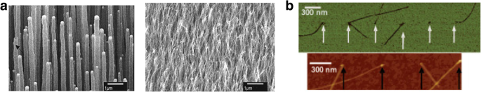
Another method of controlling the growth of CNTs is based on rapid heating (900 °C for 10 min) of catalyst nanoparticles (Fe/Mo) in the presence of feeding gas (CO/H2 ) [200,201,202]. SWCNTs were grown parallel to the direction of feeding gas flow. This work reported directional control of the CNTs grown by positioning the substrate based on the gas flow direction. The location and length of SWCNTs was controlled by using photolithography to deposit the catalysts. This method produced ultra-long, well-aligned and well-isolated SWCNTs with length of few mm (Fig. 29) in contrast to an earlier work that reported that long SWCNTs (in the range of mm) either bend or form loops [203]. Here, the growth of long and straight SWCNTs was attributed to the above described growth process also termed as a kite-based growth mechanism [201].

( a のSEM画像 ) catalyst pattern seen on oxide coated Si wafer prior to the growth of SWCNTs. Adapted from [202]. b Long, well-oriented SWCNTs grown using fast-heating growth process with Fe/Mo nanoparticles, CO/H2 900 °C for 10 min. Inset shows the magnified image of the SWCNT arrays formed. Adapted from [202]. c Well aligned arrays of SWCNTs (~ 5 SWCNTs μm −1 ) formed by CVD growth on a ST-cut quartz substrate. Adapted from [207]. d AFM image of aligned SWCNTs grown on r-plane (1 1 0 2) crystalline surfaces of sapphire. Adapted from [206]
Large scale, highly aligned SWCNTs arrays can also be grown by interactions between SWCNTs and the substrate [204,205,206,207] using atomic arrangement-programmed growth. Highly aligned SWCNTs could also be grown using Y-cut single-crystal quartz or ST-cut quartz substrates using CVD of methane at 900 °C and Fe catalyst. As shown in Fig. 29c, SWCNTs with diameters of 1 ± 0.5 nm were grown on quartz using this technique. In this method, SWCNTs were synthesized using CVD of methane at 900 °C with Fe clusters that were dispersed on the sapphire substrates. Alternatively, use of a-plane and r-plane sapphire (Al2 O 3 ) substrates led to guided growth along specific lattice directions due to the attractive interactions between nanotubes and Al atoms that are oriented in specific crystalline directions on the substrates (Fig. 29d).
CNT Forest Growth
CNT forests (or CNT arrays) are arrays of vertically aligned CNTs that offer applications in the field of sensors [208], gecko tapes [209], strong fibers [210] and electrical interconnects due to their ability to carry high current densities of ~ 10 8 A cm −1 [211, 212]. Various techniques such as use of plasma CVD, nanopatterning and flying carpets have been proposed as means of growing CNT forests [210, 213, 214]. Of these, CVD is regarded as one of the most efficient techniques to grow vertically aligned CNTs. Precise diameter control of CNT forests using pre-growth conditioning and catalyst engineering is one of the crucial parameters that influences its use in various applications [215,216,217]. In addition, control of number of layers and length of the tubes grown is also essential [218].
Growth of aligned MWCNT forests with diameters of ~ 8–15 nm was achieved using CVD in a quartz tube. Here, a Si wafer was used as a substrate, onto which a 5-nm-thick film of Fe (acting as a catalyst) was deposited using e-beam evaporation [219]. An alternate method for the fabrication of a closely packed MWCNT forest was reported using a multi-step growth method based on plasma-induced CVD technique [220]. The growth mechanism involves the following steps. First, very high-density plasma-induced catalytic nanoparticles were formed from a pre-deposited catalytic thin film. It was observed that these catalytic nanoparticles tend to aggregate at higher temperatures. In order to avoid this, the CNT nucleation process (immobilization procedure of catalytic nanoparticles) was performed and showed minimal aggregation of nanoparticles covered with graphitic carbon film. Finally, closely packed MWCNT forests were grown at a temperature of 450 °C (Fig. 30) [221, 223].

a Critical stages of CNT forest growth from a pre-deposited catalytic thin film using the multi-step plasma-induced CVD technique:formation of high-density plasma-induced nanoparticles, nucleation, and CNT forest formation. Adapted from [221]. b SEM image of the closely-packed MWCNT forest grown using plasma-induced CVD. Adapted from [222]
The direction of alignment of CNTs with respect to the substrate plays a crucial role in controlling the properties of CNTs grown. CNTs aligned vertically (i.e. perpendicular) to the substrate can be produced using porous silicon substrates with a catalyst patterned by electron-beam evaporation through shadow masks to produce MWCNT blocks. Another technique to produce these CNTs is using water-assisted CVD that produced SWCNT arrays in the order of few millimeters [135]. Here, large-scale production of dense CNT forests was reported to be possible with the help of CVD synthesis where the performance and lifetime of the catalysts was enhanced with the help of water. SWCNTs in the form of well-ordered pillars with a height of ~ 1 mm were grown from lithographically patterned catalyst islands as shown in Fig. 31 below. Alternatively, large-scale production of vertically aligned SWCNT forests is also possible using the oxygen-assisted CVD method. It was reported that the hydrogen species present during hydrocarbon CVD growth method may cause difficulties in the formation of new SWCNTs and can also potentially etch preformed SWCNTs. The introduction of oxygen during the growth process provides great control over the carbon and hydrogen ratio which is responsible for the growth of vertically aligned SWCNTs [223]. More recently, it was also shown that SWCNT forests could be grown using thermal CVD without a rectated etchant gas [224].

a 、 b SEM images of SWCNT forests grown using water assisted CVD. a SWCNT cylindrical pillars with 150 μm radius and ~ 1 mm height. Insert shows the root of a pillar. Adapted from [135]. b SWCNT sheets of 10 μm thickness. Adapted from [135]. c High-resolution TEM image of the SWCNTs grown using this method. Adapted from [135]
Another technique involves the fabrication of the CNTs within the pores or channels of a nanoporous template [160, 225, 226]. The commonly used templates are track-etch membranes, porous alumina (AAO) templates as well as various other nanoporous structures. Template-based synthesis allows the preparation of nanomaterials with a desired shape. A template is basically a structure in which the CNT networks form. Once the template is removed, it exposes a filled cavity with features similar to those of the template. After deposition, the nanotubes may be allowed to remain inside the pores of the templates, or they can be collected as a group of free nanoparticles. The template-based deposition process commonly makes use of CVD techniques, in which hydrocarbon precursors like pyrene and ethylene are exposed to elevated temperatures inside alumina templates. As the thermal deposition of the gas occurs over the entire surface of the pores, this method offers considerable control over the length and diameter of the tubes. One example of the growth of highly ordered arrays of parallel CNTs inside a hexagonally close-packed nanochannel alumina template is described below. At first, the anodization of high purity alumina was carried out, and led to the creation of a nanochannel alumina template made up of hexagonal array of channels with a diameter of 32 nm and length of 6 μm. Next, a small amount of catalyst (Co) was deposited electrochemically into the bottom of the template channels. By heating these templates at 600 °C for 4–5 h in a tube furnace in the presence of CO, then in a mixture of acetylene in nitrogen at 650 °C for 2 h, growth of highly ordered array of nanotubes was observed (Fig. 32) [160, 227]. Periodic array of nanotubes with diameters ranging from 10 nm to several hundred nm were grown by pyrolysis of acetylene on Co at a temperature of 650 °C.

a Mechanism of growth of highly-ordered arrays of parallel CNTs using nanochannel anodic alumina templates. The process begins with the anodization of high-purity aluminum on the substrate. By varying the anodization conditions, hexagonal close-packed arrays of varying diameters, densities and lengths can be formed. Adapted from [227]. b SEM image of the resulting hexagonally ordered array of CNTs fabricated using the method in (a )。 Adapted from [227]
Another method in the growth of SWCNT forests, involves the introduction of gas shower system to deliver water vapor and carbon source gas from the top of the forests, rather than traditional way of delivering from the side. This method enables parallel flow of water vapor and carbon source gas to the CNTs within the forest. This technique enables mass production of CNT forests with increased growth yield, height, carbon efficiency and scalability for large area growth [214, 228].
Macrostructure Fabrication
Fabrication and assembly of CNTs on a macroscale is of utmost importance in order to enhance its practical applications [179]. A commonly reported technique is using spin coating. This process of fabricating CNT films involves depositing droplets of CNT-based suspensions at the center of a substrate and then spinning the substrate to a very high velocity such that the CNT dispersion spreads out on the surface of the substrate, forming a thin film (Fig. 33a) [229, 230]. This process is due to the centrifugal force on the CNT dispersion. The thickness of the film depends on the viscosity of the dispersion, angular speed, spin time and the concentration of CNTs. Before the CNT dispersion is formed, it is important to overcome the Van der Waals forces between the tubes, else they will tend to aggregate and form clumps on the film. Amphiphilic surfactants are usually added to enhance the dispersibility of the tubes; conventional surfactant will not suffice because there is a strong charge repulsion between the CNT complexes and the surfactant, which prohibits the deposition of CNTs onto the substrate. Additionally, high-power ultra-sonication or strong-acid treatment is usually performed on the tubes. After the CNT film is deposited, the surfactant is usually either washed off or vaporized from the surface of the substrate. Spin coating is not applicable for large substrates because they cannot be spun at a sufficiently high rate to form an even layer. Additionally, the process lacks material efficiency as a lot of the material is flung off during spinning [229]. Alternatively, electrophoresis process can also be used for the film deposition of CNTs [231]. Some of the other relevant techniques include using composites [232], foams [233], yarns [210] and aerogels [234] as discussed below.

a Schematic of spin coating process for the fabrication of thin film of CNTs. Adapted from [230]. The corresponding SEM images of the SWCNT film prepared by single deposition of spin coating the substrate with CNT solution in an organic solvent called quinquethiophene-terminated poly (ethylene glycol). Adapted from [229]. b A schematic of a CNT-polymer composite fabrication via solution-based processing. Adapted from [232]
CNT Composites
Due to the various properties that CNT’s exhibit, especially being superior in stiffness and strength, they can be widely used in structural applications. Furthermore, researchers are showing increased interest in tapping CNT’s properties by fabricating them into a polymer matrix. Some of the commonly used CNT-based polymer composites are made up of polystyrene, ultra-high molecular weight polyethylene (UHMWPE), PMMA, epoxy and phenolic resin [62, 235,236,237]. Various techniques have been proposed for fabricating CNT-polymer composites based on the material combinations used. Some of the common methods like solution casting, melt mixing and in-situ polymerization are discussed below.
Solution casting, also referred as solvent casting, facilitates CNT dispersion, where CNTs are suspended in the desirable polymer solution via magnetic stirring or sonication (energetic agitation process). The solvent is then allowed to evaporate to produce CNT-polymer composites. Polymers such as polyvinyl alcohol (PVA) [238], PMMA [239] and epoxy [236] have been used in this method. One such manufacturing technique is shown in Fig. 33. Here, PVA/CNT composite fibers of ~ 50 μm diameter were synthesized using the following steps. First, CNTs were dispersed in ethanol, then a PVA-coated polyester strip was dipped in a solution containing the CNT mixture. Then, the CNT-coated PVA on the polyethylene terephthalate (PET) strip were delaminated. Finally, this delaminated layer was stretched and twisted to form a composite fiber (Fig. 33a). Studies involving different solutions and methods have demonstrated that the selection of solvent for nanotube dispersion had an influence on the properties of synthesized nanocomposites and the type of solvent is dependent on the solubility of polymer in it [240]. A major shortcoming of this method is that the nanotubes may agglomerate if the solvent evaporation process is slow. This may be mitigated by increasing the rate of evaporation [241]. This leads to inhomogeneous distribution of CNT’s in the polymer matrix [242].
Another commonly used method for the fabrication of CNT-polymer nanocomposites is called melt mixing. It is mostly used for manufacturing of thermoplastics and thermistors. Thermoplastic polymers melt/soften when heated to high temperatures thus making them less viscous. This causes the substrate to be less viscous and the need for high shear forces to disrupt the nanotubes bundle. In this method, composites of various polymers (such as polystyrene and polypropylene) are formed with CNTs. To start with, the selected polymers are mixed with nanotubes in a high sheer mixer. Post this, composite films are formed using compression molding [6]. Further studies in this area has enabled different techniques such as extrusion, compression molding, injection molding, etc. for fabricating samples of various shapes [6, 243, 244].
Recently, melt-mixing method was used in the manufacturing of positive temperature coefficient (PTC) thermistors using CNTs as conductive fillers in high-density polyethylene (HDPE) composites. Traditional PTCs manufactured using carbon black (CB) filled high-density polyethylene composites suffer from disadvantages like low thermal stability and poor processability. Use of CNTs in the manufacturing process can help in overcoming these challenges as the CNT-based thermistors showed ~ 129% increase in hold current and hold voltage, in comparison with the CB-filled composites [245]. These CNT/HDPE microstructure composites were prepared by melt-mixing, hot-pressing and packaging methods as shown in Fig. 34a. CNT/HDPE composites showed a decrease in electrical resistivity with an increase in the CNT loading. Figure 34b shows a comparison of current vs time plot obtained for CNT/HDPE and CB/HDPE thermistors.

a Schematic of the fabrication of CNT/HDPE thermistors using melt mixing. The process consists of melt-mixing, hot-pressing and packaging. Adapted from [245]. b Graph comparing the current vs time plots of CNT/HDPE and CB/HDPE thermistors. The comparison of the current decay between the CNT/HDPE and CB/HDPE thermistors with the same resistances under peak applied voltages shows a quick response of current delay of the CNT/HDPE thermistors. Adapted from [245]
CNTs can also be fabricated with monomers or polymers of higher molecular weight using in-situ polymerization. In general, this method can be used in the fabrication of almost any polymer composite with CNT to polymer matrix that is either covalently or non-covalently bounded [246, 247]. In addition, this method makes the grafting of larger polymer molecules to the walls of CNT possible. This enables the fabrication using insoluble and thermally unstable polymers that cannot be achieved by solution or melt processing. A stronger interaction of CNTs with polymers during the growth stage due to π-bonding was observed in this technique [248]. One such schematic of fabrication of CNTs using in-situ polymerization is shown below in Fig. 35 [249].

Schematic of formation of SWCNT/P3HT/PPy or SWCNT/P3HT/PEDOT conductive films and fibers using in-situ polymerization. The SWCNT/P3HT monomer dispersions were prepared and then coated onto a glass slide to form a film or extruded from a syringe to form fibers. Adapted from [249]
Many other lesser known methods to fabricate nanocomposites have also been proposed such as twin screw pulverization [250], latex fabrication [251], coagulation spinning [252] and electrophoretic deposition [253].
Foams, Yarns and Fibers
Three-dimensional porous networks made of polymers and CNTs have a great potential to be used in various applications like energy storage [254] and sensing [255]. Here, CNTs are used as modifiers into structures made of different porous materials like carbonaceous aerogels, foams and sponges [219, 234, 256]. Fabrication of CNT foams and aerogels can be done using several techniques like c-CVD, phase separations, polymerization reactions, etc. Creation of CNT foams and aerogels can be done using a bottom-up method consisting of phase separations induced by thermal phase transition. Here, a three-dimensional (3D) network of CNTs is initially formed in a solution, post which the liquid part is removed without disturbing this network. This technique is commonly referred as freezing as it involves a solid-liquid phase separation process. However, it was reported that CNTs grown using the various freeze-drying techniques lead to agglomerations [257].
Another technique of CNT aerogel formation is using a gas-liquid phase separation process, commonly referred to as foaming as shown in Fig. 36 [258]. Fabrication of CNT foams with controlled pore structures using this foaming process can be done using PVA, polystyrene, polyurethane, etc. [259, 260] An alternate route to the fabrication of CNT foams is using CVD, wherein, by controlling the growth parameters like type of catalyst and source of carbon, vertically aligned CNT array foams could be formed [233, 260]. Recently, aligned CNT foam structures of desired size were fabricated by stacking sheets of CNTs and infiltrating the stacked sheet assembly with pyrolytic carbon (PyC) [233]. Here, vertically aligned MWCNTs were grown using CVD technique with FeCl2 as catalyst and acetylene as the carbon precursor. These aligned CNTs were drawn from arrays and collected around two rotating parallel glass rods in order to have less compacted macro-porous structures. The CNT foams were then coated with 20 to 100 cycles of alumina buffer layers (that pins the catalyst particles on the surface of nanotubes) to help in the formation of secondary CNTs leading to creation of junctions, or branched CNT networks [260, 261]. In this method, prior to CVD, a buffer layer made of Al2 O 3 is deposited onto the porous structure to promote secondary CNT growth (in the form of straight CNTs or coiled-CNTs) at the surface of the primary nanotubes and within the pores of the CNT foams [261].

CNT foam formation using various techniques. The figure depicts various phase separation processes being performed on a CNT suspension to produce the CNT foam. The phase separation process is usually done via a gas-liquid phase separation or a solid-liquid phase separation as shown in the figure. Adapted from [258]
MWCNTs shaped into yarns have potential to be used in multifunctional applications like artificial muscles and actuators, in electronic textiles and as fiber-based supercapacitors [219]. Electromechanical actuators formed using sheets of SWCNTs (as electrolyte-filled electrodes of a super capacitor) are reported to have shown higher stresses than natural muscle. Like natural muscles, the macroscopic actuators are assemblies of billions of individual nanoscale actuators and are shown to have a great potential in various applications [39, 262, 263]. In addition, by twisting CNTs from a MWCNT forest, CNT yarns could be formed [219, 264]. Here, MWCNTs with a diameter of ~ 10 nm were drawn from a MWCNT forests (grown using CVD by using Fe catalyst) and twisted with a motor running a variable speed of ~ 2000 rpm [219]. This twisting causes the MWCNTs to form small individual bundles consisting of few CNTs. Further, by allowing the twisted yarns to relax (untwist in an opposite twist direction), knitted and knotted yarns were formed (Fig. 37a–c) [265,266,267]. Alternatively, MWCNT yarns could be synthesized from aerogels during CVD [268]. MWCNTs can also be drawn into sheets from MWCNT forests synthesized using CVD with ~ 3 nm iron film as a catalyst and acetylene or ethylene as carbon source [269]. These sheets were formed as a highly anisotropic electronically conducting aerogels that could be drawn into sheets with ~ 50 nm thickness as shown in Fig. 37d [270].

SEM and optical images of CNT yarns. a SEM image of a part of CNT yarn from the nanotube forest being drawn and twisted. Dry spinning of the CNT yarns from the forests (vertically grown CNT array) is shown. Adapted from [266]. b SEM image of a knotted CNT yarn. Adapted from [265]. c Optical image of a MWCNT knitted yarn, with a glass rod through the center. The average diameter of the MWCNT knitted yarn was measured to be 34.09 ± 2.86 μm. Adapted from [267]. d SEM image of MWCNTs in a forest being drawn into a sheet. Adapted from [270]
Recently, electrically conducting 3D fabrics made from hybrid Spandex (SPX)–MWCNT yarns showed excellent stretchable properties with a potential to be used as artificial muscles (Fig. 38). They were fabricated in a knitting machine into which a CNT aerogel sheet drawn from CNT forest, wrapped around continuous supply of SPX filament was fed. These fabrics exhibited breaking strains of 600% to 900%, tensile strengths in the range 75 to 86 MPa and an approximate resistance of 3.0 kΩ m −1 [271]. They offer unique advantages such as large tensile actuation, high repeatability, scalability and stretchability due to which they can be used in various applications like medical sensors/devices and smart clothing.

SEM image of CNT/SPX8 knitted textile and the corresponding mechanical properties. a SEM image of CNT/SPX8 knitted textile. Adapted from [271]. b Stress–strain curves of the CNT textile material. Adapted from [271]. c Strain versus time for this textile, stretched for 1000 cycles at 0.2 Hz. Adapted from [271]
Alignment/Placement on Substrates
Most methods of CNT mass production result in randomly oriented CNT bundles. The placement and alignment of the tubes can either be done while they are being grown or after they have been grown. In the former, the CNTs are grown in a given direction and position within the substrate or normal to it, while in the post-growth method, the tubes are first isolated in a dispersion and then the dispersed CNTs are aligned and selectively positioned in a certain direction by applying external forces. Various methods have been used for aligning and placement of CNTs on substrates, as discussed below.
Photolithography
Photolithography has been successfully used to prepattern either catalysts or substrates for site-selective growth of CNTs. In such a case, the photolithography setup consists of a substrate (glass), a patterned resist and a photomask. The process involves the following steps; first, direct photolithographic patterning is performed on the metal-containing photoresist. Next, metal oxides are heated and then reduced by hydrogenation to patterned metal nanoparticles, which act as catalysts from which aligned CNTs are grown, via the hydrocarbon pyrolysis of FePc (Fig. 39a, b) [272]. Alternatively, catalyst patterning using photolithography can be done by creating a template with desired patterns of photoresist, followed by molding of PET stamps which are used in transfer printing of CNTs. However, this technique suffers from certain limitations which include not having the necessary resolution to grow nanometer-scale patterns. In addition, growth of CNTs may be hindered/affected due to contamination that may be introduced through these masks [195].

a Schematic flow diagram of micropattern formation of vertically aligned MWCNT arrays by direct photolithography process. Adapted from [272]. b SEM images of patterned films of vertically aligned MWCNT arrays formed by the pyrolysis of FePc onto a photolithographically patterned quartz substrate. The resolution of the figure is in the micrometer scale. Adapted from [272]. c Step-by-step illustration of transfer printing of SWCNTs onto various substrates by contact stamping. Adapted from [273]
Transfer Printing
Currently, most nanoelectronics devices are being made on flat, rigid, smooth surfaces. This poses a problem because future nanoelectronics applications will require for nanomaterials to be placed on flexible substrates, such as plastic, or nonplanar materials. Due to this, methods such as transfer printing, which allow for the fabrication of a device on a conventional substrate and then transfer-printing of the entire working device onto target substrates, are being developed [273, 274]. This precludes the need for performing harsh synthesis and fabrication methods on the target substrate. The mechanism for transfer printing CNTs is as follows; first, the tubes are stabilized by mixing them with surfactant molecules, next the surfactant-stabilized CNTs are deposited on a variety of substrates from the solution. The most common process for the deposition of the tubes with wide area coverage is based on controlled flocculation. The controlled flocculation approach uses a spinning mechanism, in which the suspension of tubes and a solvent (methanol) are applied at the same time, to a spinning substrate. The methanol or any other hydrophilic solvent displaces the surfactant from the nanotubes, by bonding to them thereby causing the tubes to precipitate from the solution, to the edges of the substrate where they are deposited on a high-resolution polydimethylsiloxane (PDMS) stamp. The tubes form thick films on the PDMS stamps, and the stamp can be pressed on the target substrate to transfer the tube patterns from the raised regions of the stamp (Fig. 39c) [273]. One problem with this technique is the requirement to pattern the stamps each time based on the design [275].
Template-Based Deposition
Patterning in thin film CNTFET channels can be achieved with an inexpensive solution-based self-assembled colloidal mask that leads to devices with large on/off ratios while maintaining carrier mobility and sub-threshold performance. By guiding SWCNT thin film formation, the colloidal mask approach allows an ordered nanoscale CNT network with more consistent and accessible channel surface area resulting in patterned thin film FET channels whose structure and properties can be tuned for different applications (such as sensors). In one of the template-based deposition techniques, the patterned SWCNT thin films were fabricated using colloidal lithography [241]. This method employed a liquid-based self-assembly of colloidal sphere monolayers as masks to create ordered nanoscale arrays and films. Here, heavily doped silicon wafers with ~ 100-nm-thick SiO2 layer was used as a substrate and patterning of Au/Ti source-drain electrodes with ~ 40 nm thickness and 1–3 μm spacing on the surface of wafer was carried using photolithography. SWCNT powder (1.2–1.5 nm diameter and 2–5 μm length) was dispersed in chloroform with SDS surfactant to form aqueous suspensions, which was mixed with an aqueous suspension of silica or polystyrene colloidal spheres to form patterned nanotube networks. The overall process flow for patterning the SWCNT thin films and the corresponding results are illustrated in Fig. 40a–c.

a Schematic of fabrication process for patterned CNTFET networks. b Optical microscope image of patterned electrode substrates after self-assembled colloidal mask assembly. c SEM image of interconnected nanotube ring patterns formed during the self-assembly process and gate voltage-dependent I - V characteristics of resulting CNTFET. The center to center distance of the circles is around 500 nm. (Inset) shows the corresponding magnified view of the interconnected nanotube ring patterns. [Y. Chen and C. Papadopoulos, unpublished results]
Another technique to control the placement, alignment and spacing of CNTs is achieved using DNA-origami structures [276,277,278]. Here, various geometrical shaped (L-, T-, Y-, rectangular, triangular, etc.) nanotube structures are formed on DNA-origami templates using self-assembly process (Fig. 41), where the CNTs were organized into several patterns, with control over the inter-tube angles. In one of the techniques, CNTs solubilized by wrapping with ssDNA reacted with the DNA origami constructs forming linear arrays of ssDNA that lead to immobilization of the CNTs onto the DNA origami scaffold. This was due to the strong π–π interaction existing between the bases of ssDNA and CNTs. SWCNTs with lengths ranging from ~ 92 ± 24 nm (termed as short SWCNTs) and ~ 314 ± 249 nm (termed as long SWCNTs) were obtained in this work [276].

Schematics of a rectangular DNA-origami. Adapted from [276]. b 、 c Site-specific immobilization of ssDNA-wrapped short and long CNTs onto the single rectangular DNA-origami scaffold. Adapted from [276]. d AFM images of DNA origami-nanotubes formed using self-assembly showing CNTs aligned at the edges. Adapted from [276]. e AFM images of DNA origami-nanotubes formed using self-assembly showing two single rectangular DNA-origamis aligning two long 6,5-SWCNTs. Adapted from [276]. f Cross-shaped SWCNTs. Scale bar equals 100 nm. Adapted from [276]
Solution-Based Deposition of CNTs
Most solution-based alignment or deposition methods of CNTs require the formation of CNT films from CNT suspensions. As such, there’s a need to form uniform dispersions of CNTs in a solvent. A challenge that is commonly encountered in dispersing CNTs is overcoming the strong inter-tube interaction of CNTs, which is attributed to van der Waals forces. When CNTs are placed in a solvent, they usually bundle together. This attractive force of the CNTs is usually overcome by binding the CNT walls to surfactant molecules (surfactant wrapping) to form stable solutions of CNTs. As such, these van der Waals forces are a major consideration when using solution-based methods for aligning CNTs [230]. Some of the solution-based alignment techniques are discussed below.
Inkjet printing is a precise method of patterning, and therefore, post-printing steps are not needed. This technique is advantageous because it does not require the use of a prefabricated template, thereby allowing for rapid printing at a low cost [279, 280]. Additionally, it is valuable because many layers of ink can be printed on top of one another. The carbon nanotube ink is prepared following certain steps; first, sonication is used to disperse the CNTs within the liquid. After dispersing the CNTs, the ink is centrifuged several times to separate the well-dispersed CNTs from the bundles, which could clog the printer nozzle. Next the supernatant is collected and filtered severally to remove any remaining CNT bundles. After the ink has been successfully produced, it is loaded into an inkjet cartridge and ready to be used for printing on substrates like glass and polymers.
Consumer inkjet printers are of two types; continuous and drop-on-demand. The former supplies a continuous stream of ink droplets, which are charged once they leave the nozzle, and are then deflected by voltage plates, such that the applied voltage determines if the droplet will be deposited on the substrate, while the drop-on-demand printer functions in a different manner, in that, the printer only ejects ink when required [279]. Carbon nanotube inkjet printing has been successfully used to deposit MWCNTs and SWCNTs. It has also been used to fabricate transistors, sensors and electroluminescent devices. The process is a useful development in electronics because it allows direct printing of the CNTs to make a pattern or a circuit on a suitable substrate, thereby enabling us to control the transparency and resistance of the printed patterns (Fig. 42a) [281]. In order to produce uniform networks of CNTs by inkjet printing, the jetting conditions need to be properly tuned to generate correctly directed droplets. Another important consideration is the temperature of the substrate. The substrates need to be heated in order to reduce the drying time for the printed CNT solution. For manufacturing purposes, quick drying of the dropped ink is desirable. However, the temperature should not be too high as it would cause the droplet to evaporate once it is released from the nozzle. A constraint in using this process is the difficulty of dispersing nanomaterials within the ink as CNTs typically bundle together in a solvent, due to their attractive van der Waals forces. The bundling of tubes needs to be prevented as it could cause clogging of the inkjet nozzle [279].

a Optical image of a CNT-based circuit on polyimide wrapped around a test tube. The circuit was fabricated using CNT inkjet printing. Adapted from [281]. b Schematic of the Langmuir-Blodgett (LB) process for the fabrication of films. The LB process is either performed using the b vertical dipping method or c horizontal lifting method. Adapted from [283]
Alternatively, spray-coating involves spraying CNTs dispersed in a suspension on a heated substrate such that every sprayed droplet undergoes pyrolytic decomposition when it reaches the hot substrate surface thereby forming a thin layer of CNTs film [282]. CNT films can be spray deposited on glass before being transferred to a flexible substrate or they could be directly sprayed onto the flexible substrate. Before the spraying of the CNTs can take place, the solution has to be prepared. First, CNTs in powdered form are dispersed into a solvent via sonication. The CNTs are usually either dispersed in an organic solvent or in a surfactant-based aqueous dispersion. Surfactant-based dispersion using SDS or carboxymethyl cellulose (CMC) is usually preferred because the surfactants can be rinsed off after the film is deposited, as these surfactants are soluble in water. The surfactant is first dissolved in water to form an aqueous solution, to which the CNTs are later added. This forms a surfactant based aqueous CNT solution. Sonication of the surfactant-based solution is then performed to evenly disperse the CNTs. Finally, the solution is centrifuged, and the supernatant is taken from the top to be used for deposition. Before spray deposition of the CNTs can occur, the substrate surface has to be treated and cleaned using solvents like acetone and isopropanol, followed by plasma cleaning. After treatment of the substrate, the colloidal suspension of CNTs is sprayed through an air atomizing spray gun, onto a heated substrate. The dispersing fluid (in this case, the surfactant) then evaporates due to the heating of the substrate to leave behind a uniform coating or layer of CNTs.
CNT films can also be produced using the Langmuir-Blodgett (LB) technique, in which a substrate is dipped in a solution containing well-dispersed CNTs, and then slowly pulled out either by horizontal lifting or by vertical dipping method as shown in Fig. 42b, c [283]. This technique produces a thin layer of CNTs aligned in the dipping direction on the substrate. The thickness of the CNT film is dependent on the concentration of CNTs in the solution, the pulling speed, and the number of dips. Generally, SWCNTs are dispersed in an amphiphilic polymer matrix, spread on a water surface [284]. This film is transferred to a substrate by dipping the substrate in it. The disadvantage of this method, as with most solution-based methods, is that the solution might require a solvent that is incompatible with some substrates, for example plastic.
Well-aligned, horizontal arrays of semiconducting nanotubes can also be created using nanoscale thermocapillary effects in thin-film organic coatings (Fig. 43a, b) [285]. In this method, metallic SWCNTs are selectively removed via thermal resist exposure and etching. SWCNTs, grown on quartz substrates comprise of both semiconducting and metallic nanotubes with diameters between 0.6 and 2 nm. By means of thermal evaporation, thin organic thermocapillary resist layer of a,a,a′-tris (4-hydroxyphenyl)-1-ethyl-4-isopropylbenzene is deposited on these SWCNT arrays. Post this, by etching metallic CNTs are removed from the arrays.

a Schematic illustration of steps involved in selective removal of metallic CNTs using thermocapillary effects. Adapted from [285]. b Corresponding AFM images of each step starting from growth of SWCNT arrays, followed by deposition of thermocapillary resist and etching of metallic SWCNTs. Adapted from [285]. c Schematic of the deposition of well-aligned CNTs on HfO2 by means of the ion exchange process. Adapted from [286]. d Corresponding AFM image of the nanotubes deposited on a HfO2 trench with a width of about 200 nm. Adapted from [286]
Alternatively, aligned CNTs were deposited on a HfO2 trench with a density of 10 9 cm −2 using self-assembly (Fig. 43c, d) [286]. This was done through the SDS-wrapped CNTs dispersed in water and the use of 4-(N -hydroxycarboxamido)-1-methylpyridinium iodide (NMPI) to form surface monolayer. This led to ion exchange between Na + in SDS and I − in NMPI. By controlling the concentrations of SDS surfactant and dimensions of the trenches, placement of CNTs inside the trench was randomly varied. With trenches of dimensions, 200 nm and 500 nm fabrication of a billion nanotubes per square centimeter is predicted. For example, one preliminary successful functioning CNT computer circuitry was self-assembled using selective surface chemistry [287].
Emerging Applications and Challenges
Figure 44a gives an overall summary and comparison of the various CNT assembly techniques presented in this review. As seen throughout the preceding sections, CNTs have gained widespread interest for use in applications [1, 39, 52, 57, 65, 66, 276, 288]. Electronic devices, sensors, drug delivery, energy storage devices, crypto primitives and tissue engineering are just some of the potential areas where nanotubes can be employed (Fig. 44b).

a Summary description of CNT assembly and integration techniques. b Overview of various emerging applications of CNTs
CNTs are used in various commercial applications in the form of conductivity enhancement/control in plastics [289], in anti-static packaging and to enhance the strength of concrete, polymers, baseball bats, bicycles, etc. [62, 289]. In addition, use of CNTs for structural monitoring in aircraft structures is currently patented [290]. Successful use of CNTs in this application may greatly reduce the risk of an in-flight failure caused by structural degradation of aircraft.
CNTs are also finding use in biomedical applications such as imaging [291,292,293], tissue engineering as scaffolds for bone growth [294, 295] and scaffolds to guide neurite outgrowth [296] as shown in Fig. 45a–c. In addition, CNTs can also to be used in targeted drug delivery systems (Fig. 45d) [297, 298] due to their capabilities to interact with mammalian cells. Due to their ability to penetrate into cell membranes, CNTs can be used as carriers to deliver therapeutic agents into the cytoplasm of cells. CNTs that are gastrointestinally absorbed were lysosomotropic and could enter into the cells for targeted drug delivery.

a SEM image of bone-tissue sections observed 4 weeks after CNTs were implanted into tubal defects in mice. Adapted from [295]. b 、 c SEM images showing guided neurite growth along the MWCNT array pattern. The bottom image in part (c ) represents the magnified view of a selected region in the top image. Adapted from [296]. d Schematic of steps showing CNT-based drug delivery systems. CNTs of various lengths were used as drug carriers by making their ends open and allowing the drug to be loaded for targeted drug delivery. Adapted from [297]
As mentioned previously, a major class of applications of CNTs is in electronic devices like FETs [46, 48, 299] and to build integrated circuits (ICs) and flexible electronics [300, 301]. Some of the other applications include their use in batteries, where a CNT film was used as the current collector for a lithium ion battery [302], in transparent conductive films that can be used in flat panel displays such as laptops and cameras [57, 303], hydrogen storage to be used as fuel source [304], as interconnects [305, 306] that can potentially offer advantages over copper (due to their high thermal stability and large current carrying capacity), in non-volatile random access memory for molecular computing [307] and in thin-film solar cells made up of a semi-transparent thin film of nanotubes on a n-type crystalline silicon substrate, wherein CNTs films are used as photogeneration sites and are also used for enhancing conductivity (Fig. 46a, b) [308].

a Schematic of a thin-film CNT solar cell. Adapted from [308]. b J–V characteristics of a CNT solar cell with area = 2.15 cm 2 (in red) and area = 0.06 cm 2 (in black). Adapted from [308]. c Schematic of a randomly connected 2D nanotube array that can be used as a crossbar switch. Here, CNTs self-assemble in the HfO2 trenches with width of 70–300 nm. Adapted from [314]. d Schematic of an s-SWCNT-based wearable array of electronic devices, consisting of memory units, capacitors and logic circuits that can be integrated into different circuits for day-to-day applications. Adapted from [317]
Due to their unique thermal and mechanical properties, CNTs have also found applications as nano additives in heat conductive materials made of CNT-based lubricating oils, nanoliquids, etc. [309] These additives can be used for heat dissipation in electronic devices like LEDs and computer processors [309,310,311]. The high thermal conductivity of CNTs also enables their use as thermally conductive composites that could potentially replace metallic parts in devices such as electric motors and generators [14, 312, 313].
In addition, CNTs have also been tested to create an unclonable electronic random structure to create cryptographic keys that can be a used to provide significantly higher level of security as compared to the conventional binary-bit architecture with the same key size [314, 315]. A schematic of generation of random bits based on two-dimensional (2D) carbon nanotube arrays is shown in (Fig. 46c). In this method, well-aligned CNTs are deposited on a HfO2 trench, ~ 7 nm high using self-assembly. This was done through the SDS-wrapped CNTs dispersed in water and the use of NMPI to form a surface monolayer, which led to ion exchange between Na + in SDS and I − in NMPI. By controlling the concentrations of SDS surfactant and dimensions of the trenches, placement of CNTs inside the trench was randomly varied. Further, CNT thin films, also known as CNT mats, have shown potential to be used in radio-frequency signal transmission [316]. A combination of most of the above applications includes the use of CNTs in wearable electronics consisting of many memory units, capacitors, transistors and logic circuits, etc. (Fig. 46d) [317]. In one of the recent examples, stretchable and ultrathin wearable array of electronic devices with a dimension of ~ 3 μm showed a possibility to be integrated on the human skin. Techniques such as spin coating, thermal evaporation and photolithography were used to fabricate these devices based on the required application.
Use of aligned/organized CNTs in the form of yarns, forests and sheets can help in further development of CNTs for large-scale industrial applications. Some of the emerging applications of CNTs include their use as multi-functional coating materials, which in turn can be used as an alternative to environmentally hazardous paints containing biocides [288]. CNTs have also proven useful in anticorrosion coatings in metals (showing enhanced strength and coating stiffness) [318], and in transparent electronics like flexible displays. Due to their ability to be manufactured as metallic, semi-conducting or wide-band gap CNTs, they can also be used in manufacturing new generation electronic components and devices like batteries, supercapacitors, transistors, logic circuits, memristors, neuromorphic computing, sensors for optics, gas, pressure, glucose, tumor detection, electronic textiles, artificial muscles and electro-thermal actuators, etc. [1, 219, 297, 307, 319, 320]. CNTs have a potential to be used in other applications in the form of wires in nanoscale very-large-scale integrated (VLSI) circuits [306], to fabricate flexible and foldable sheets [321], fibers via wet spinning [264, 322], in energy and water treatment [323].
Despite their numerous advantages and potential applications, several outstanding issues related to CNTs must still be addressed in order for their potential to be fully realized in the future (cf. Fig. 44a):For example, low mechanical strength and thermal conductivity of the typical as-grown CNT material has to be studied and improved. In addition, during the growth of long nanotubes tubes with closed ends are also formed due to the presence of pentagonal and heptagonal defects in the graphene lattice. This makes it difficult for their use in many applications where access to open-ended tubes is needed, e.g. to functionalize and/or contact the tube ends. Also, controlling chirality of the CNTs grown, which critically influences the electrical properties of the nanotubes is still considered a major challenge. Growing high purity, well-aligned semiconducting CNTs is one of the important steps for realization of various applications and thus far, growth of CNTs with very few metallic CNTs for thin films and devices is yet to be fully realized. Since the choice of catalyst plays a significant role in the growth of CNTs, further research on different materials that can be used as catalysts is necessary to understand issues arising due to the tube-catalyst interactions. A major obstacle to commercial implementation of CNT (or graphene) nanoelectronics is rooted in the lack of an efficient and reliable method of device production and integration (cf. silicon integrated circuits). In addition, CNT electronics will likely have to compete with the emergence of silicon nanowires and related structures for integrated circuits in the near future as the rapid pace of Moore’s Law continues along with evolution and advances in semiconductor electronics and CMOS technology. Continued focus on the other allotropes of carbon like graphene (for 3D CNT-graphene networks used in, e.g. thermal interfaces) and fullerenes is necessary which may help in wide scale production and/or improvement in the properties of existing CNTs. For applications requiring macroscopic amounts of nanotubes, well-ordered assemblies will allow optimization of desired properties with nanoscale control. Lastly, since CNTs have not yet been fully used in large-scale commercial applications, not much is known about their possible effects on the human health and the surrounding environment [324] both during processing, post-processing and disposal [325,326,327]. Studies focusing on these aspects will also be necessary.
結論
The superb (and unique) properties of CNTs and their potential use in a wide range of applications has led researchers to consider nanotubes based on carbon as one of the emerging materials that may play key roles in the future of nanoscale-based applications. This is supported by the CNT-related patent statistics between 2000 and 2017 (Fig. 47). In this review, we have focused on the progress made in the field of CNT fabrication, purification, assembly and integration of single and multiple tubes for their use in various applications. We discussed how structural control of individual CNT properties such as chirality, diameters and junctions are important factors in determining their properties (structural, electrical, mechanical, thermal properties and cost) and to utilize them for various applications. Also included is information related to post-growth purification techniques of CNTs using methods such as selective surface chemistry, gel chromatography and density gradient centrifugation. Assembly and integration for multiple CNTs using forest growth, catalyst patterning and composites are discussed. Details of their alignment/placement onto different substrates using methods such as photolithography, transfer printing and different solution-based techniques are also included. Towards the end, we list some emerging applications like sensors, field-effect devices, energy storage devices, health monitoring in aircraft structures, crypto primitives, commercial applications in the form of conductivity enhancement/control in plastics, in bio-based applications like tissue engineering, drug delivery, etc. based on their unique properties, advantages and challenges that need to be understood for efficient utilization of these structures in the future.

Trends in CNT-related patents filed worldwide between 2000 and 2017. Data collected from European Patent Office’s webpage using keywords ‘carbon nanotubes or carbon nanotube or graphene’
Significant progress has been made over the past two decades in CNT fabrication and assembly, from individual tubes to large ensembles and commercial applications should continue to grow as well-organized CNT materials are introduced. In terms of nanoscale integration, precise control of CNT type, placement and orientation will enable many applications in electronics and photonics and beyond, and despite challenges, continued advances in CNTs, with their almost ideal one-dimensional structure and properties, and related structures will play an important role in future applications of nanotechnology.
データと資料の可用性
該当なし。
略語
- 1D:
-
一次元
- 2D:
-
二次元
- 3D:
-
三次元
- AC:
-
交流
- AFM:
-
原子間力顕微鏡
- CB:
-
Carbon black
- c-CVD:
-
Catalytic chemical vapor deposition
- CMC:
-
Carboxylmethyl cellulose
- CNTFET:
-
Carbon nanotube field-effect transistor
- CNT:
-
カーボンナノチューブ
- CVD:
-
化学蒸着
- DC:
-
直流
- DEP:
-
誘電泳動
- DGU:
-
Density gradient ultracentrifugation
- DNA:
-
デオキシリボ核酸
- DOS:
-
状態密度
- FCCVD:
-
Floating catalyst chemical vapor deposition
- FET:
-
電界効果トランジスタ
- HDPE:
-
High-density polyethylene
- ICs:
-
Integrated circuits
- IEX:
-
Ion-exchange chromatography
- IR:
-
赤外線
- LB:
-
Langmuir-Blodgett
- LCDs:
-
Liquid crystal displays
- m-SWCNTs:
-
Metallic single-walled carbon nanotubes
- MWCNT:
-
多層カーボンナノチューブ
- N-CNTs:
-
Nitrogen-doped CNTs
- NIL:
-
Nano-imprint lithography
- NMPI:
-
4-(N-hydroxycarboxamido)-1-methylpyridinium iodide
- PBA:
-
Prussian blue analog
- PDMS:
-
ポリジメチルシロキサン
- PECVD:
-
プラズマ化学気相成長法
- PET:
-
ポリエチレンテレフタレート
- PMMA:
-
ポリメチルメタクリレート
- PTC:
-
Positive temperature coefficient
- PVA:
-
ポリビニルアルコール
- PyC:
-
Pyrolytic carbon
- SDS:
-
ドデシル硫酸ナトリウム
- SEM:
-
Scanning electron microscopy/microscope
- SPX:
-
Spandex
- SSA:
-
比表面積
- ssDNA:
-
Single-stranded-deoxyribonucleic acid
- s-SWCNTs:
-
Semiconducting single-walled carbon nanotubes
- SWCNT:
-
単層カーボンナノチューブ
- TEM:
-
透過型電子顕微鏡
- THz:
-
Terahertz
- TPU:
-
Thermoplastic polyurethane
- UHMWPE:
-
Ultra-high molecular weight polyethylene
- UV:
-
紫外線
- VHS:
-
Van Hove singularities
- VLS:
-
Vapor-liquid-solid
- VLSI:
-
Very-large-scale integrated
- VPE:
-
Vapor phase epitaxy
- VSS:
-
Vapor-solid-solid
ナノマテリアル
- センサーとプロセッサーは、産業用アプリケーション向けに統合されています
- 最近の論文では、カーボンナノチューブのスケーラビリティ、統合のブレークスルーについて詳しく説明しています
- シクロカーボンの作成とイメージング
- カーボンナノチューブヤーン、マッスル、透明シート
- 材料:自動車用ガラスおよび炭素繊維強化PP
- 改善された診断および治療用途のための多機能金ナノ粒子:レビュー
- 合成および生物医学的応用のための蛍光ナノ材料の進歩と挑戦
- ソルベイは、海洋石油およびガス用途向けの高性能カーボンファイバーテープを発売
- 産業用冷凍および産業用冷却アプリケーション用のドライブ
- ボーリングおよびターニングアプリケーション用のスイング旋盤
- Box Build Assembly のレイアウトとトレース ルール