


新規の調整可能な二元超格子としてのダブルゲートナノヘリックス
要約
帯電したワイヤとしてモデル化された2つの平行なゲート間のナノヘリックスに閉じ込められた電子の問題を理論的に調査します。ダブルゲートナノヘリックスシステムは、ゲート電圧に非常に敏感な特性を持つバイナリ超格子です。特に、バンド構造は、ゲート電圧の特定の組み合わせに対してエネルギーバンド交差を示します。これは、準相対論的なディラックのような現象につながる可能性があります。直線偏光および円偏光によって引き起こされる光学遷移の分析は、ダブルゲートのナノヘリックスを多用途のオプトエレクトロニクスアプリケーションに使用できることを示唆しています。
はじめに
筆頭著者が子供の頃に熱心に収集した化石化した螺旋状の腹足類から、間違いなくかつてこれらの先史時代の生き物を定義したDNAの絡み合った構造まで、らせんの幾何学は自然全体に広がっています[1]。自然界に存在する生体分子の形状に起因する複雑な機能に触発され[2–6]、ナノテクノロジーに適したらせん形状を有する他のシステムは、豊かな物理学を生み出し、新しいアプリケーションに貢献することが期待されます。過去30年間で、ナノファブリケーション技術の目覚ましい進歩により、InGaAs / GaAs [7]、Si / SiGe [8]、ZnO [9–11]、CdS [9–11]などのさまざまなシステムでナノヘリックスが実現しました。 12]、SiO 2 / SiC [13、14]、純炭素[15–20]、およびII-VIおよびIII-V半導体[21](現在の最新技術については参考文献[21–26]を参照)。その結果、トポロジカルな量子化されたチャージポンピング[27、28]、超伝導[29]、スピンフィルタリング[30–32]などのエキゾチックな輸送特性から、分子およびナノメカニカル伸縮性電子機器[33、 34]圧電効果[35]、センシングアプリケーション[36、37]、エネルギー[38]および水素貯蔵[39]、および電界効果トランジスタ[40、41]による。
ナノヘリックスベースのデバイスの魅力は、最終的にはヘリックス構造のトポロジーにエンコードされた固有の周期性に由来します。特に、ナノヘリックスを横電界(ヘリックス軸に垂直)にさらすと、超周期的ポテンシャル上での電子のブラッグ散乱などの超格子挙動が生じ、超格子ブリアンゾーンの端でエネルギーが分裂します。電界によって線形に調整可能な最低の状態[42、43]。この振る舞いは、ブロッホ振動と負の微分コンダクタンスをもたらす可能性があり[44、45]、ヘリックスを介したスピン偏極輸送を強調し[31、46]、ナノフォトニックキロプチカルアプリケーションで有用な円二色性の強化をもたらします[47]。このシステムは、単一の超格子を構成し、さらに、ナノヘリックスをトンネルダイオードまたはガンダイオードとして使用して、周波数の増倍、増幅、およびユーロ化されたテラヘルツ範囲の放射線の生成または吸収を行う可能性を開きます[48–51]。プロトタイプの超格子は通常、固有のバンドギャップが異なる交互の半導体層のヘテロ構造で実現されますが、ナノヘリックス超格子のパラメータは外部電界によって完全に制御されます。反対に、以前の従来の超格子ポテンシャルの形状は、ヘテロ構造に固有であり、堅牢である一方で、大きな外部場を使用せずに、その利用の過程で操作する能力が制限されています。したがって、これの代わりに超格子としてナノヘリックスを使用することの魅力は、それらのより優れた調整可能性にあります。
一方、ヘテロ構造の半導体超格子(または実際には光格子の超格子構造[52–55]と光格子の冷原子[56、57])を使用すると、単純な量子井戸を超えて、より複雑な超格子ユニットセルを作成できます。らせんに沿った電界。バイナリ超格子[58–60](これにより、ユニットセルは2つの異なる量子井戸および/または障壁によって区別されます)への拡張でさえ、ブロッホツェナー振動[61]などの豊富な物理学を約束します。調整可能なビームスプリッターおよび干渉計アプリケーション[62]。したがって、ナノヘリックスベースの超格子の外部磁場調整可能性と、バイナリ超格子の優れた機能性を組み合わせることが非常に望ましいでしょう。
以下では、らせん軸に位置合わせされた2本の平行にゲートされた帯電ワイヤの間にナノヘリックスが配置された、まさにそのようなシステムについて説明します。追加の横電界の適用を想定し、ゲートおよび電界制御可能な電位が一次元らせんに沿った二元超格子を構成することを理論的に示しています。
メソッド
理論モデル
N を備えた単一電子半導体円形ナノヘリックスの事例を研究することから始めましょう。 半径の回転 R 、ピッチ p 、および全長 L = Np 。ナノ構造は、螺旋軸が z に沿って整列した、帯電したワイヤとしてモデル化された2つの平行なゲートの間に配置されます。 -軸と、軸とゲートがすべて図1に示すように同じ平面上にある場合。さらに、ゲート軸平面に垂直な外部横電界を考慮します\(\ mathbf {E} =E _ {\ bot} \ハット{\ mathbf {y}} \)これは、平面の下のポテンシャルに対する平面の上のポテンシャルの反射対称性を破るために使用できます。 r を介してパラメトリックに記述されたらせん座標で作業します =( x、y 、 z )=( R cos( s φ )、 R sin( s φ )、ρ φ )、ここで動的角度座標φ = z / ρ ρのらせんの軸に沿った距離のみに依存します = p / 2 π 、および s =±1は、それぞれ左巻きまたは右巻きのらせんを示します。この作業では、左巻きのらせん s を検討します。 =1。有効質量モデルの枠組みでは、エネルギースペクトルε ν νの このような外部ポテンシャルの影響下にあるヘリックス内の電子の固有状態は、シュレディンガー方程式から求められます。
$$-\ thinspace \ frac {\ hbar ^ {2}} {2M ^ {*} \ rho ^ {2}} \ frac {d ^ {2}} {d \ varphi ^ {2}} \ psi _ {\ nu} + \ left [V_ {g}(\ varphi)+ V _ {\ bot}(\ varphi)\ right] \ psi _ {\ nu} =\ varepsilon _ {\ nu} \ psi _ {\ nu} $$(1 )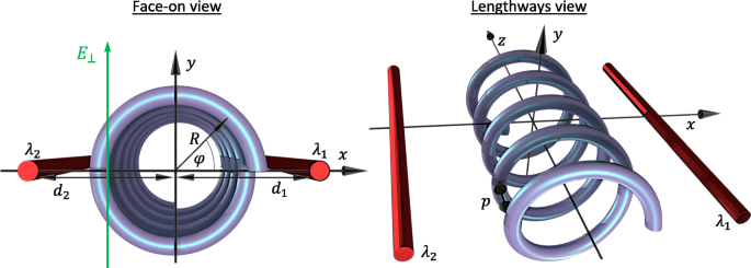
正面と縦方向の両方の観点からのシステムのジオメトリとパラメータの図。 R はらせん半径であり、 d 1 および d 2 は、電荷密度λのらせん軸からの帯電ワイヤの距離です。 1 およびλ 2 、 それぞれ。空間座標φ らせんの正面からの角位置を表し、 z に関連しています。 -φを介して調整 =2 π z / p p で らせんのピッチ。横電界 E ⊥ y と並行して適用されます -軸
ここで、電子の有効質量 M を幾何学的に繰り込みました。 e M へ ∗ = M e (1+ R 2 / ρ 2 )らせん軸に沿った座標ですべてを表現するために(φを思い出してください) = z / ρ )これは外部電位にとってより便利です。ここでは、 V ⊥ (φ )=− eE ⊥ R sin(φ )は、 y に沿って方向付けられた横電界からの寄与です。 - V のような軸 ⊥ (π / 2)<0。ゲートからの電位は V g (φ )=− e [Φ 1 (φ )+ Φ 2 (φ )] Φによって与えられる個々の帯電したワイヤーのために、らせんに沿って電子が感じる静電ポテンシャル i (φ )=− λ i k ln( r i / d i )。ここで、 i =1,2はワイヤにラベルを付け、λ i はワイヤの線形電荷密度であり、\(k =1/2 \ pi \ tilde {\ epsilon} \)と\(\ tilde {\ epsilon} \)の絶対誘電率です。特定のワイヤからのテスト電荷の垂直距離は、\(r_ {i} =[d ^ {2} _ {i} + R ^ {2} + 2(-1)^ {i} d_ {i } R \ cos(\ varphi)] ^ {1/2} \)、 d i らせんの軸までのワイヤーの対応する距離を示します。ゼロゲート誘起電位をらせんの軸に沿って定義しました。総一次元ポテンシャル V T (φ )= V g (φ )+ V ⊥ (φ )は明らかに周期的です V T (φ )= V T (φ +2 π n )期間2 π 一般的に(これは p の期間に対応します 座標 z に関して )。この期間は原子間距離よりも大幅に長く、典型的な超格子効果を引き起こします。この文字は、横電界( V で再現可能)のナノヘリックスとは異なります。 T (φ )= V ⊥ (φ )ここで)主に、ダブルゲート電位 V を介して超格子の繰り返されるユニットセルを操作することによって g (φ )。限界を超える p →0、2つの静電ゲート[63、64]の対象となるリング画像上の粒子に戻ります。近似を行う R / d i ≪1、 V を展開する場合があります g (φ )cos(φの2次まで )、そして式を変換すると1無次元の形になります
$$ {\ begin {aligned} \ frac {d ^ {2} \ psi _ {\ nu}} {d \ varphi ^ {2}} + \ left [\ epsilon _ {\ nu} + 2A_ {g} \ cos( \ varphi)+ 2B_ {g} \ cos(2 \ varphi)+ 2C _ {\ bot} \ sin(\ varphi)\ right] \ psi _ {\ nu} =0、\ end {aligned}} $$(2)エネルギースケールの単位での量\(\ varepsilon _ {0}(\ rho)=\ hbar ^ {2} / 2 M ^ {*} \ rho ^ {2} \)は
として定義されます $$ \ begin {array} {@ {} rcl @ {}} A_ {g}&=&\ beta \ frac {\ left(d_ {1} ^ {2} + R ^ {2} \ right)} { d_ {1} R}(1- \ gamma)、\ qquad B_ {g} =\ frac {\ beta} {2} \ left(1+ \ frac {\ lambda_ {1}} {\ lambda_ {2}} \ gamma ^ {2} \ right)、\\ C _ {\ bot}&=&e E _ {\ bot} R / 2 \ varepsilon _ {0}(\ rho)、\ qquad \ qquad \ qquad \; \ epsilon _ {\ nu} =\ frac {\ varepsilon _ {\ nu}} {\ varepsilon_ {0}(\ rho)}。 \ end {array} $$(3)ここで、\(\ beta =ek d_ {1} ^ {2} R ^ {2} \ lambda _ {1} / 2 \ left(d_ {1} ^ {2} + R ^ {2} \ right)^ {2} \ varepsilon _ {0}(\ rho)\)は、ゲート1からの寄与を特徴付けますが、非対称パラメーター\(\ gamma =\ lambda _ {2} d_ {2} \ left(d_ {1} ^ {2 } + R ^ {2} \ right)/ \ lambda _ {1} d_ {1} \ left(d_ {2} ^ {2} + R ^ {2} \ right)\)は、ゲート2からの相対的な寄与を示します、γを使用 =1は、ポテンシャルへの等しいゲート寄与に対応します(結果として A g =0)。 d を維持することの難しさによって引き起こされる避けられない非対称性に注意する必要があります 1 = d 2 λを操作することで補正できます 1 およびλ 2 。この手紙では、γの検討に限定しています。 ≤1(これは| Φです 1 |> | Φ 2 |)1より大きい非対称パラメータは、ゲートにラベルを付けるインデックスの単純な交換とそれに対応する視点のシフトφを介して、1未満の同等のシステムにマッピングできます。 →φ ±π 。 C のみも考慮します ⊥ 負の C の対称性により、≥0 ⊥ φでのそのような座標変換に関して 、および A g ≥0、 B g > 0(つまり、ワイヤの正電荷密度のみβ> 0)負に帯電したゲートを持つ潜在的な風景は、正に帯電したゲートからのパラメータの正しい組み合わせで再現できるため。図2に、無次元ポテンシャル V をプロットします。 T (φ )/ ε 0 (ρ )、πの強さで - B に固定された周期ポテンシャル成分 g =0.2、2倍の周期の摂動パラメータのいくつかの組み合わせ A g および C ⊥ 。総外部ポテンシャルがφに沿って二元超格子を誘導することがわかります 、青色で強調表示されたユニットセルとしての二重量子井戸(DQW)。これは、相対的なゲート寄与を操作することにより、質的に異なる形をとることができますγ および横電界 E ⊥ 。ユニットセルは、基本的に同等のゲート寄与(γ)の下でシングルウェルです。 =1)横電界なし E ⊥ =0( A の図2aのように g = C ⊥ =0)。 E の修正 ⊥ =0、ゲート1の寄与が強い(γ <1)、ユニットセルは異なるウェルの最小値と縮退したバリアの最大値を持つDQWになります(図2b、ここで A g =0.1および C ⊥ =0)。対照的に、DQWの最小値を縮退させ、2つの潜在的な障壁を相互に操作するには、対称的なゲートの寄与(γ)が必要です。 =1)ゼロ以外の電界 E ⊥ ≠0( A を使用した図2c g =0および C ⊥ =0.1)。非対称ゲート寄与の組み合わせ(γ <1) E を使用 ⊥ ≠0は、ポテンシャル井戸の最小値とバリアが異なるDQWを生成します(図2dに示すように、両方の A g = C ⊥ =0.1)。これにより、次のセクションで説明するように、質的に異なり、豊かな行動につながります。
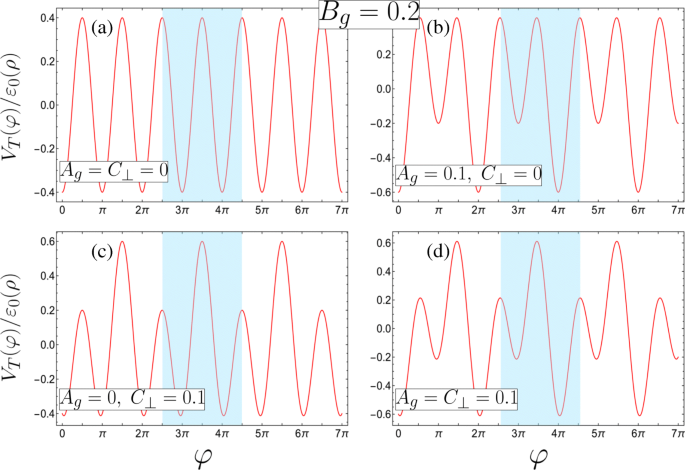
ユニットセルが青色で強調表示された4つの可能な超格子ポテンシャル構成(無次元パラメーターで定義。物理パラメーターの対応する要件については式3を参照、すべて B g =0.2)。 a ユニットセルに縮退した最小値と最大値を持つ単項超格子( A g = C ⊥ =0)。 b – d b のいずれかから形成されたバイナリ超格子 縮退した最大値( A )により、いずれかの最小値について最小値と内部反射対称性が異なる非対称DQW g =0.1、 C ⊥ =0)、 c 縮退した最小値のみを持つ対称DQW( A g =0、 C ⊥ =0.1)、または d 最小値と最大値が異なる非対称DQW( A g = C ⊥ =0.1)
無限行列としてのソリューション
式の解2はブロッホ関数の観点から見つけることができます
$$ \ psi_ {n、q}(\ varphi)=(2 \ pi N \ rho)^ {-\ frac {1} {2}} e ^ {iq \ varphi} \ sum_ {m} c ^ {( n)} _ {m、q} e ^ {im \ varphi}、$$(4)ここで、 q = k z ρ 電子の準運動量 k の無次元形です z らせんの軸に沿って、 n サブバンドを示し、プリファクターはφに関する正規化から生じます。 :\(\ rho \ int _ {0} ^ {2 \ pi N} | \ psi _ {n、q}(\ varphi)| ^ {2} d \ varphi =1 \)。結果の式に\(e ^ {im ^ {\ prime} \ varphi} / 2 \ pi \)を掛け、φに関して積分することにより、指数関数の直交性を利用します。 、ここで m ' は整数であるため、係数\(c ^ {(n)} _ {m、q} \)、
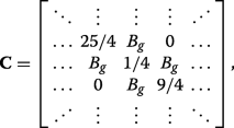
の連立方程式は無限になります。 $$ {\ begin {aligned}&\ left [(q + m)^ {2}-\ epsilon_ {n} \ right] c ^ {(n)} _ {m}-\ left(A_ {g}- i C _ {\ bot} \ right)c ^ {(n)} _ {m-1}-\ left(A_ {g} + i C _ {\ bot} \ right)c ^ {(n)} _ {m +1} \\&\ quad- B_ {g} \ left(c ^ {(n)} _ {m + 2} + c ^ {(n)} _ {m-2} \ right)=0、\ end {aligned}} $$(5)わかりやすくするために、 q -添え字表記が削除されました、ε n、q ≡ε n および\(c_ {m} ^ {(n)} \ equiv c_ {m、q} ^ {(n)} \)。式5は、システムが q で周期的であることが明らかな無限の5対角行列を表します。 、および-1 /2≤ q で定義される最初のブリルアンゾーンに考慮を制限する場合があります ≤1/ 2。超格子ポテンシャルがない場合 A g = B g = C ⊥ =0の場合、固有値は m によって列挙されます。 εによって与えられる m =( m + q ) 2 m を認識します らせん上の自由電子に関連する角運動量量子数である。式からわかります。 5 A のとき g = C ⊥ =0はΔの状態のみ m =±2が混合されているのに対し、 A を介して達成される、ウェルの最小値またはバリアが異なるDQWユニットセルの形成 g ≠0および/または C ⊥ ≠0、状態をΔと混合します m =±1。興味深いことに、外部の横方向のポテンシャル(ヘリックスの1回転で変化する)の下でのヘリックス上の電子のシステムは、磁場が貫通し、角度座標に沿って変化する同じ関数形式。例えば参考文献を参照してください。 [65–67]または、たとえばRefsを比較します。 [42–45]と[68–70]。リングの場合、 q が果たす役割 ここで磁束が吸収されます。したがって、この研究でのまったく同じ分析が、磁束によって貫通されるリングであるダブルゲート量子リング[63–66]の問題に適用できます。
式(1)に対応する行列を切り捨てて数値的に対角化します。 5は n を提供します サブバンド固有エネルギーε n q の各値の係数\(c_ {m} ^ {(n)} \) 。 | m で切り捨てを適用します | =10、マトリックスサイズを大きくしても、最下位のサブバンドに感知できるほどの変化が生じないことを知っていれば安全です。
結果と考察
ダブルゲートナノヘリックスバンド構造
図3に、パラメータのいくつかの組み合わせに対する最低帯域のエネルギー分散をプロットします。超格子の形状に応じて、分散挙動に顕著な変化が見られます。パラメータの特定の組み合わせについては、ブリルアンゾーンの端(図3aおよびc)またはブリュアンゾーンの中心(図3bおよびd)。
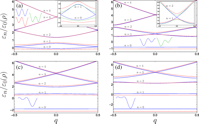
無次元パラメータのさまざまな組み合わせに対するダブルゲートナノヘリックスシステムのバンド構造( B を使用) g =0.4全体で固定): a 青一色(赤の破線)のプロット A g =0& C ⊥ =0( A g =0.2& C ⊥ =0)、挿入図はさらに、 A の横電界を受ける下の2つのサブバンドの動作をプロットします。 g =0& C ⊥ 一点鎖線の緑色の曲線として=0.2。 b 青一色(赤の破線)のプロット A g =0.63& C ⊥ =0( A g =0.8& C ⊥ =0)青い曲線がブリルアンゾーンの中心で交差するエネルギーバンドを伴う共鳴の最初の入射(テキストを参照)を示している場合、挿入図は、下部で励起された2つのサブバンドの動作を A g =0.63& C ⊥ 一点鎖線の緑色の曲線として=0.2。 c 青一色(赤の破線)のプロット A g =1.26& C ⊥ =0( A g =1.5& C ⊥ =0)ここで、青い曲線は、より高い帯域のブリルアンのエッジでエネルギーギャップが閉じている2番目の共鳴の入射を示しています。 d 3番目のレゾナンス以上のサブバンドミニギャップは中央で閉じ、青一色(赤の破線)が A g =1.9& C ⊥ =0( A g =2.2& C ⊥ =0)。ユニットセルの形状がスケッチされています、 n バンドを列挙し、挿入図の軸はメイングラフと同じです
低磁場の2倍の周期の摂動
A の場合 g = C ⊥ =0の場合、ユニットセルは2つの同等の量子井戸を構成し、その結果、ブリルアンゾーンの端に接触するバンドのペアの出現が自然に発生します。実際、ユニットセルを1つだけ使用すると、超格子期間が半分になり、ブリュアンゾーンが2倍になります-1≤ q ≤1。次に、通常の単項超格子バンド図を観察します。ここでは、 q での地面と最初のバンドの間のバンドギャップが示されています。 =1は、 n 間のバンドギャップを介してここで与えられます =1および n q で=2 =0であり、 B では線形になります g 摂動論から。それでも、バンド構造の説明は| q にあります。 付録の行列代数を使用したDQWユニットセル画像の| =1/2。図3aの挿入図に見られるように、二重周期ポテンシャル項のいずれかを導入すると、ブリルアンゾーンの端にバンドギャップが開きます。対称ゲート寄与からのユニットセル( A g =0)横方向の場 C の適用下で、対称DQWの形式を保持します。 ⊥ らせんゲート軸に垂直で、一方のポテンシャル障壁がもう一方に対して変更されています(図3aの緑色のDQWスケッチで示されています)。 C ⊥ バンドギャップを開くと、分散の変更は、適用された A の同様の大きさからの変更よりも著しく感度が低くなります。 g 。これは、| q のバンドギャップが小さいことからわかります。 | =図3aの挿入図の緑色の一点鎖線の場合は1/2( A を使用) g =0および C ⊥ =0.2)赤い破線の曲線( A の場合)の大きなギャップと比較して g =0.2および C ⊥ =0)。この振る舞いを強調するために、図4aは| q でのエネルギーギャップサイズをプロットしています。 | =1/2 2つの最下位サブバンド間\(\ Delta \ varepsilon _ {01} ^ {(q =1/2)} / \ varepsilon _ {0}(\ rho)\)固定 B g =0.25(両方の C の関数として) ⊥ ( A g =0)および A g ( C ⊥ =0)、それぞれ一点鎖線の緑と一点鎖線の赤の曲線として。ゼロ横電界および非対称ゲート電位( C ⊥ =0および A g ≠0)の場合、ユニットセルは非対称DQWになりますが、同等の障壁があるため、どちらかのウェルの最小値について内部反射対称性があります。そうすれば、 A の変化に対するバンドギャップの感度が高いことがわかります。 g 超格子が構築される孤立したDQWユニットセルの特性を考慮することによって。 A を使用 g = C ⊥ =0、| q で | =1/2(ブリルアンゾーンの端)、地面から形成されたブロッホ状態と、孤立したDQWユニットセルの最初の励起状態(図4aの青い概略図と付随する波動関数を参照)は、任意のフェーズ。この状況は、図3aのギャップのない青色の分散曲線に対応します。緑のDQWスケッチを介して図4aに概略的に示されているように、 C ⊥ DQWの最小値は縮退したままですが、一方のバリアの相対的な最大値をもう一方のバリアに対して減らします。このように、孤立したDQWの基底状態は、より小さなポテンシャル障壁の下での確率分布のわずかな増加によってのみ変更され(摂動されていない基底状態と比較してエネルギーがわずかに低下するだけです)、最初の励起状態は本質的に変化しません。そのノードはバリアの下に配置されており、その変動に敏感ではないためです。これらの基底状態と最初の励起状態から構築されたブリルアンゾーンの端にあるブロッホ状態は、小さい方の障壁の下での基底状態の波動関数の減衰が少ないという点でのみ、摂動されていない場合と異なります(緑色のDQWと青色のDQWを比較してください。図4a)。 A の変更 g バリアを縮退させたまま、DQW最小値の相対位置を操作します。 2つの最も低い孤立したDQW状態の波動関数はかなり異なり、基底状態は特異なより深い井戸の局所的な基底状態に向かう傾向があり、最初の励起状態はより浅い井戸の局所的な基底状態に向かう傾向があります[71]。摂動は基底状態のエネルギーを低下させますが、最初の励起状態のエネルギーは、 A の増加に伴って浅い井戸の最小値が上にシフトするため、比較的増加します。 g 、その結果、 A に対するバンドギャップサイズの感度が高くなります。 g 。特に、基底サブバンド内の粒子は、 A の増加に伴い、最も深いポテンシャル井戸の底部近くに急速に閉じ込められます。 g 。したがって、最低帯域は、横電界の場合よりも速く分散のないフラットバンドに近づき、高密度の状態密度に伴う電子的不安定性と強い相互作用効果につながる可能性があります[72]。
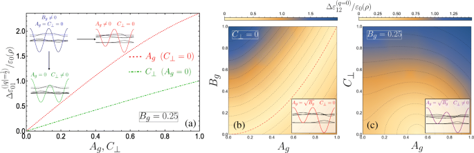
a A の関数としてのグラウンドと最初のサブバンド間のバンドギャップサイズ g ( C ⊥ )赤の破線(緑の一点鎖線)としてプロットされます。ここでは B g =0.25。これらの図は、孤立したDQWユニットセルと固有状態に対するさまざまな摂動の影響を示しています。 b – c 2D密度プロットを介して示される第1サブバンドと第2サブバンド間のバンドギャップサイズ。 b A g および B g C の場合 ⊥ =0、および c A g および C ⊥ 固定の B g =0.25。 b 隣接する等エネルギー線は0.17の差を示し、\(A_ {g} =\ sqrt {B_ {g}} \)の赤い一点鎖線でギャップがゼロになり、 c 差は0.13で、最小の半円の輪郭(0.5,0)の中心にギャップがありません。ダイアグラムは、分離されたDQWと固有状態をスケッチします。 s 間でハイブリダイゼーションは発生しません -likeおよび p - b の共鳴局在化した個々のウェル状態のように 、ただし c で行います 電界によって一方のバリアが他方のバリアに対して変化するため
エネルギーバンドの交差
C を維持すると、非常に注目に値します。 ⊥ =0および A を増やします g 、最初はすべての縮退が解除されますが、その後の高エネルギーバンドは、ブリルアンゾーンの中心と端の間で交互に交差するようになります(図3aからdに進む青と破線の赤の曲線が交互に現れる動作を観察してください)。物理的には、ユニットセル内の局所的な波動関数の相互作用の観点から、消失するバンドギャップを理解することができます。非対称DQWポテンシャルが、浅い井戸の基底状態( s -軌道のように)は、より深い井戸( p )の最初の励起状態と共鳴します。 -軌道のように)、 q =0いずれかのウェルの中心の周りの反射対称性により、これらの状態の反対のパリティは、それらの間の通常のトンネル結合を妨げ、その結果、これらの軌道から構築された励起状態は一致します(図3bの青い曲線)。これは、いわゆる s を彷彿とさせます − p 光格子の共鳴[73、74]。同様に、パラメータが浅いウェルの局所的な基底状態が同じパリティを持つ深いウェルの励起状態と共鳴するようなものである場合、| q | =1/2の場合、ブロッホ相の存在により、これら2つの隣接する局在ウェル状態間の通常の混成が完全に抑制され、バンドギャップが閉じます(2番目の励起状態での地面の共鳴について図3cに示すように)。周期的ポテンシャルからの散乱の言葉で; cos(φからの2次ブラッグ散乱振幅の完全な破壊的干渉により、バンドギャップは閉じられます。 )cos(2 φからのポテンシャルおよび1次散乱振幅 )潜在的な[75–77]。
式(1)に戻ることにより、ブリルアンゾーンの中心と端の両方でエネルギーバンド交差(ゼロ横電界の場合)の存在を定量的に示すことができます。 2、これは C のときにWhittaker-Hillの式として認識できます。 ⊥ =0 [78]。ブロッホ関数式。 4ねじれた周期境界条件に従うψ n、q (φ +2 π )=exp(2 π iq )ψ n、q (φ )。特に、 q の場合 =0式の正式な解。 2は2 πです -周期的ですが、| q | =1/2の解は2 πです -反周期的(したがって、4 πを検索します -定期的な解決策)。具体的には、式。 2 C ⊥ =0は、波動関数を方程式の漸近解の積として表現することにより、準正確に解けるInceの方程式[79、80]にマッピングできます。 2および未知の関数\(\ psi _ {n、q}(\ varphi)=\ exp \ left [-2 \ sqrt {B_ {g}} \ cos(\ varphi)\ right] \ Phi _ {n、 q}(\ varphi)\)、そのような
$$ \ frac {d ^ {2} \ Phi_ {n、q}} {d \ varphi ^ {2}} + \ frac {\ xi} {2} \ sin(\ varphi)\ frac {d \ Phi_ { n、q}} {d \ varphi} + \ frac {1} {4} \ left [\ eta_ {n、q} --p \ xi \ cos(\ varphi)\ right] \ Phi_ {n、q} =0、$$(6)ここで、補助パラメータ\(\ xi =8 \ sqrt {B_ {g}} \)、ηを定義しました。 n、q =4 ε n、q +8 B g 、\(-p \ xi =8A_ {g} + 8 \ sqrt {B_ {g}} \)、およびΦ n、q (φ )各解の必要なねじれた周期性を維持します(ここで p に注意してください) ではない らせんピッチ)。さらに、ここでの超格子ポテンシャルは変換φの下で不変であるため →− φ 、 q のソリューション =0および q =1/2は、次の三角級数のように、奇数パリティと偶数パリティに分けることができます
$$ \ Phi_ {n、0} ^ {(e)}(\ varphi)=\ sum_ {l =0} a ^ {(n)} _ {l} \ cos(l \ varphi)、$$(7a )$$ \ Phi_ {n、0} ^ {(o)}(\ varphi)=\ sum_ {l =0} b ^ {(n)} _ {l + 1} \ sin [(l + 1)\ varphi]、$$(7b)$$ \ Phi_ {n、\ frac {1} {2}} ^ {(e)}(\ varphi)=\ sum_ {l =0} \ widetilde {a} ^ {( n)} _ {l} \ cos \ left [\ left(l + \ frac {1} {2} \ right)\ varphi \ right]、$$(7c)$$ \ Phi_ {n、\ frac {1} {2}} ^ {(o)}(\ varphi)=\ sum_ {l =0} \ widetilde {b} ^ {(n)} _ {l + 1} \ sin \ left [\ left(l + \ frac {1} {2} \ right)\ varphi \ right]、$$(7d)正式な解決策をカバーし、 q の解決策に注意します =−1/2は q の場合と同じです =1/2。ここでは、上付き文字 e および o 関数にそれぞれ偶数と奇数のラベルを付け、 n まだ n を指します n でもあるサブバンド これらの指定された q の固有状態 値。これらを式に代入します。 6は、フーリエ係数の3項漸化式になります。 q =0偶数の解は
を生成します $$-\ eta_ {n、0} ^ {(e)} a ^ {(n)} _ {0} + \ xi \ left(\ frac {p} {2} +1 \ right)a ^ {( n)} _ {2} =0、$$(8a)$$ \ xi pa ^ {(n)} _ {0} + \ left(4- \ eta_ {n、0} ^ {(e)} \ right)a ^ {(n)} _ {2} + \ xi \ left(\ frac {p} {2} +2 \ right)a ^ {(n)} _ {4} =0、$$(8b )$$ {\ begin {aligned}&\ xi \ left(\ frac {p} {2} --l +1 \ right)a ^ {(n)} _ {2l-2} + \ left(4l ^ { 2}-\ eta_ {n、0} ^ {(e)} \ right)a ^ {(n)} _ {2l} \\&\ quad + \ xi \ left(\ frac {p} {2} + l +1 \ right)a ^ {(n)} _ {2l + 2} =0、\ qquad(l \ ge 2)\ end {aligned}} $$(8c)q の奇数解に対応する漸化式 =0は
です $$(4- \ eta_ {n、0} ^ {(o)})b ^ {(n)} _ {2} + \ xi \ left(\ frac {p} {2} +2 \ right)b ^{(n)}_{4} =0, $$ (9a) $$ {\begin{aligned} &\xi \left(\frac{p}{2} - l +1 \right)b^{ (n)}_{2l-2} + \left(4l^{2} - \eta_{n,0}^{(o)} \right)b^{(n)}_{2l} +\xi \left(\frac{p}{2} + l +1 \right)b^{(n)}_{2l+2}\\ &=0. \qquad (l \ge 2) \end{aligned} } $$ (9b)q =1/2 even solution gives
$$ \left[ 1 -\eta_{n,\frac{1}{2}}^{(e)} +\frac{\xi}{2}(p+1) \right]\widetilde{a}^{(n)}_{1} +\frac{\xi}{2}(p+3)\widetilde{a}^{(n)}_{3}=0, $$ (10a) $$ {}{\begin{aligned} &\frac{\xi}{2}(p-2l +1)\widetilde{a}^{(n)}_{2l-1}+\left[(2l+1)^{2} - \eta_{n,\frac{1}{2}}^{(e)}\right]\widetilde{a}^{(n)}_{2l+1}\\ &\quad+ \frac{\xi}{2}(p+2l+3)\widetilde{a}^{(n)}_{2l+3}=0, \qquad (l \ge 1) \end{aligned}} $$ (10b)and the q =1/2 odd solution gives
$$ \left[ 1 -\eta_{n,\frac{1}{2}}^{(e)} -\frac{\xi}{2}(p+1) \right]\widetilde{b}^{(n)}_{1} +\frac{\xi}{2}(p+3)\widetilde{b}^{(n)}_{3}=0 $$ (11a) $$ {}{\begin{aligned} &\frac{\xi}{2}(p-2l+1)\widetilde{b}^{(n)}_{2l-1}+\left[(2l+1)^{2} -\eta_{n,\frac{1}{2}}^{(e)}\right]\widetilde{b}^{(n)}_{2l+1}\\&\quad + \frac{\xi}{2}(p+2l+3)\widetilde{b}^{(n)}_{2l+3}=0. \qquad (l \ge 1) \end{aligned}} $$ (11b)Consider then Eqs. (8c) and (9b) for the q =0 solutions. The series solutions (7a) and (7b) can clearly be made to terminate if p is 0 or an even positive integer. The resulting polynomials are referred to as Ince polynomials. The remaining solutions for higher eigenvalues are simultaneously double degenerate and correspond to the energy crossings observed at q =0 for certain parameters. The existence of these degeneracies can be seen by looking at the diagonalizable matrices describing the recursion relations for a l および b l :
$$ \boldsymbol{\mathcal{A}} =\left[ \begin{array}{ccccc} 0 &\xi\left(\frac{p}{2} +1 \right) &0 &0 &\hdots \\ \xi p &4 &\xi\left(\frac{p}{2} +2 \right) &0 &\hdots \\ 0 &\xi\left(\frac{p}{2} - 1 \right) &16 &\xi\left(\frac{p}{2} +3 \right) &\hdots \\ \vdots &\vdots &\vdots &\vdots &\ddots \end{array} \right]\!, $$ (12)and
$$ \boldsymbol{\mathcal{B}} =\left[ \begin{array}{ccccc} 4 &\xi\left(\frac{p}{2} +2 \right) &0 &0 &\hdots \\ \xi\left(\frac{p}{2} - 1 \right) &16 &\xi\left(\frac{p}{2} +3 \right) &0 &\hdots \\ 0 &\xi\left(\frac{p}{2} -2 \right) &36 &\xi\left(\frac{p}{2} +4 \right) &\hdots \\ \vdots &\vdots &\vdots &\vdots &\ddots \\ \end{array} \right]\! $$ (13)それぞれ。 Either of the above tridiagonal matrices can be broken into tridiagonal sub-matrices if a leading off-diagonal matrix element is equal to zero, i.e. if p is an even number. The matrices will decompose into two tridiagonal blocks, one smaller finite matrix \(\boldsymbol {\mathcal {A}_{1}}\) (\(\boldsymbol {\mathcal {B}_{1}}\)) and a remaining infinite matrix \(\boldsymbol {\mathcal {A}_{2}}\) (\(\boldsymbol {\mathcal {B}_{2}}\)). From the theory of tridiagonal matrices the corresponding eigenvalue spectra for each matrix is then \(\eta (\boldsymbol {\mathcal {A}}) =\eta (\boldsymbol {\mathcal {A}_{1}}) \cup \eta (\boldsymbol {\mathcal {A}_{2}})\) and \(\eta (\boldsymbol {\mathcal {B}}) =\eta (\boldsymbol {\mathcal {B}_{1}}) \cup \eta (\boldsymbol {\mathcal {B}_{2}})\). The smaller finite matrices are analytically diagonalizable in principle, giving exact eigenvalues, and their corresponding finite length eigenvectors define the fourier coefficients yielding Ince polynomials via Eq. 7. We can see that for a given even integer p , the remaining infinite tridiagonal matrices are the same \(\boldsymbol {\mathcal {A}_{2}}=\boldsymbol {\mathcal {B}_{2}}\equiv \boldsymbol {\mathcal {D}}\) which results in the double degenerate eigenvalues. To be clear, we provide an example of when p =2 in the Appendix.
In the same way, when p is a positive odd integer the series solutions (7c) and (7d) can be made to terminate, and the matrices corresponding to \(\widetilde {a}_{l}\) and \(\widetilde {b}_{l}\) share eigenvalues resulting in the closing of higher subbands at the edge of the Brillouin zone q =± 1/2. From the definitions of the auxiliary parameters in Eq. 6, we have
$$ A_{g} =(p+1)\sqrt{B_{g}}, $$ (14)which defines the condition for exactly-solvable solutions for the lower lying solutions and simultaneously the existence of higher double degenerate eigenvalues above the p th subband, with p =0 or an even positive integer corresponding to crossings at the centre of the Brillouin zone, while crossings at the edge require p to be an odd positive integer. Figure 4b plots the size of the band gap between the first and second subbands \(\Delta \varepsilon _{12}^{(q=0)}/\varepsilon _{0}(\rho)\) as a function of A g および B g , with the dot-dashed red contour line corresponding to Eq. 14 for p =0。 The schematic indicates the appropriate eigenstates of the isolated DQW at the p =0 resonance.
The application of a small transverse field C ⊥ breaks the reflection symmetry of the system, permitting hybridization of the localized well states of the isolated DQW which results in a significant change at points of degeneracy, as can be seen by comparing the schematic depicted in Fig. 4b with that in c (see also inset of Fig. 3b). We plot in Fig. 4c the behaviour of the band gap between the first and second subbands as a function of A g および C ⊥ 。 Here we see that the band gap is more sensitive to C ⊥ due to the significant change in the isolated DQW eigenstates by lowering one barrier with respect to the other. This behaviour is notably the converse of the parameter sensitivity for the band gap between the ground and first subbands. By degenerate perturbation theory, it can be shown that this induced band gap is linear in C ⊥ for the lowest crossing bands when p =0, and to higher order with increasing p 。 Finally, within the vicinity of the crossings, e.g. for small q about q =0 in Fig. 3a, the dispersions could be approximated as a quasi-relativistic linear dispersion yielding Dirac-like physics, which could permit superfluiditiy [81] for example. The advantage in using nanohelices lies in introducing such phenomena to portable nanostructure based devices, while also exhibiting unusual responses of the charge carriers to circularly polarized radiation [44, 45, 82–85] (or indeed magnetic fields [86, 87]) due to the helical spatial confinement.
Optical transitions
In order to understand how our double-gated nanohelix system interacts with electromagnetic radiation, we study the inter-subband momentum operator matrix element \(T^{g\rightarrow f}_{j} =\langle {f}|\boldsymbol {\hat {j}} \cdot \boldsymbol {\hat {P}}_{j} |{g}\), which is proportional to the corresponding transition dipole moment, and dictates the transition rate between subbands ψ f and ψ g 。 Here, \(\boldsymbol {\hat {j}}\) is the projection of the radiation polarization vector onto the coordinate axes (j =x,y 、 z ) and the respective self-adjoint momentum operators are [44, 45, 82–84]
$$ \boldsymbol{\hat{P}}_{x} =\boldsymbol{\hat{x}}\frac{i \hbar R}{\rho^{2} +R^{2}}\left[\sin(\varphi)\frac{d}{d\varphi} + \frac{1}{2}\cos(\varphi) \right], $$ (15a) $$ \boldsymbol{\hat{P}}_{y}=-\boldsymbol{\hat{y}}\frac{i \hbar R}{\rho^{2} +R^{2}}\left[\cos(\varphi)\frac{d}{d\varphi} - \frac{1}{2}\sin(\varphi) \right], $$ (15b) $$ \boldsymbol{\hat{P}}_{z}=-\boldsymbol{\hat{z}}\frac{i \hbar \rho}{\rho^{2} +R^{2}}\frac{d}{d\varphi}. $$ (15c)In terms of the dimensionless position variable φ , we are required to evaluate \(T^{g\rightarrow f}_{j} =\rho \int _{0}^{2\pi N}\psi _{f}^{\ast } P_{j} \psi _{g} d\varphi \), and upon substituting in from Eq. 4 we find
$$ {\begin{aligned} T^{g\rightarrow f}_{x} &=\frac{i \hbar R}{2\left(\rho^{2} + R^{2} \right)}\sum_{m} c_{m}^{\ast (f)} \left[ c_{m-1}^{(g)} \left(q+m-\frac{1}{2}\right)\right.\\ &\quad\left.-c_{m+1}^{(g)} \left(q+m+\frac{1}{2}\right) \right], \end{aligned}} $$ (16a) $$ {\begin{aligned} T^{g\rightarrow f}_{y} &=\frac{\hbar R}{2\left(\rho^{2} + R^{2} \right)}\sum_{m} c_{m}^{\ast (f)} \left[ c_{m-1}^{(g)} \left(q+m-\frac{1}{2}\right)\right.\\&\left.\quad+c_{m+1}^{(g)} \left(q+m+\frac{1}{2}\right) \right], \end{aligned}} $$ (16b) $$ T^{g\rightarrow f}_{z} =\frac{\hbar \rho}{\left(\rho^{2} + R^{2} \right)} \sum_{m} c_{m}^{\ast (f)} c_{m}^{(g)} (q+m). $$ (16c)We see from Eqs. 16a and 16b that light linearly polarized transverse to the helix axis couples coefficients with angular momentum differing by unity Δ m =± 1, whereas from Eq. 16c, linear polarization parallel to the helix axis couples only Δ m =0。 In Fig. 5, we plot the absolute square of the momentum operator matrix element between the lowest three bands for linearly polarized light propagating perpendicular to the helix axis (i.e. with z -分極)。 Initially, for A g = C ⊥ =0, transitions between the ground and first bands are forbidden (as is to be expected for a unit cell with two equivalent wells resulting in a doubling of the first Brillouin zone, so it is in fact the same band). As the strength of the doubled period potential A g is increased with respect to B g , transitions become allowed away from q =0 as can be seen from Fig. 5a (following behaviour from the dotted red curve through to the solid blue curve). The parameters are swept through a resonance as we go from the solid to the dashed blue curve, wherein the situation changes drastically. To understand this behaviour, we must consider the special case of q =0。 As we traverse this resonance, the energy of the Bloch function with q =0 constructed from the first excited state of the deeper well in the DQW unit cell (p -like) passes below the Bloch function constructed from the ground state in the shallower well (s -like). Consequently, the parity with respect to φ (which is a good quantum number only for q =0 or |q |=1/2) of the two excited states is exchanged resulting in the rapid switch from forbidden to allowed at q =0, wherein the z -polarized inter-subband matrix element becomes non-zero due to the operator \(\boldsymbol {\hat {P}}_{z}\) (see Eq. 15c) now coupling the even ground state with the odd first excited state. We therefore see the opposite behaviour for transitions between the ground and second band in Fig. 5b about q =0。 While initially increasing A g allows transitions at q =0 between the ground state and the second excited state when it is p -like, beyond resonance (when the order of the s -like and p -like excited states are swapped) transitions are suppressed. See for example Ref. [88] for a clear picture of this interchange between the ordering of the even and the odd parity excited states. For transitions between the first and second band (Fig. 5c), we observe a large transition centred about q =0 due to the lifting of the m =± 1 degenerate states of the field-free helix by the superlattice potential. The presence of symmetry-breaking C ⊥ ruins the pristine parities of the states at the centre of the Brillouin zone and all transitions are allowed, as shown in the insets of Fig. 5.

Square of the dimensionless momentum operator matrix element between the g th and f th subbands in the first Brillouin zone as a function of the dimensionless wave vector q of the electrons photoexcited by linearly z -polarized radiation and for a variety of parameter combinations spanning the first incident of resonance. The different blue curves keep A g =0.5 and C ⊥ =0 fixed and vary B g =0.1, 0.2, and 0.3 corresponding to dot-dashed, dashed, and solid. The different red curves keep B g =0.3 and C ⊥ =0 fixed while varying A g =0.05, 0.1 and 0.3 as dot-dashed, dashed, and solid, while the dotted blue (dotted red) plots the limiting case A g =0.5 &B g →0 (A g →0 &B g =0.3). a Transitions between the ground and first bands. The inset plots the behaviour for fixed A g =0.5 and changing B g crossing the resonant condition at B g =0.25 (see text) in a reduced q -range, ranging from upper blue B g =0.245, lower blue B g =0.249, upper purple B g =0.251, to lower purple B g =0.255. The dashed green curves are for small non-zero transverse field C ⊥ =0.05 ranging from B g =0.245 (upper curve) to B g =0.255 (lower curve) in increments of 0.05. b Plots transitions between the ground and second bands, the inset plots the behaviour close to resonance when A g =0.5; blue is B g =0.249, purple is B g =0.251, and dark green is at resonance with C ⊥ =0.05. c Plots transitions between the first and second bands, the parameters for the inset are the same as those in (b )
In Fig. 6, we plot the absolute square of the momentum operator matrix element for right-handed circularly polarized light which propagates along the helix axis, given by |T x +iT y | 2 。 Notably, we observe a large anisotropy between the two halves of the first Brillouin zone, while the result for left-handed polarization is a mirror image to what we see in Fig. 6. Physically, this can be attributed to the conversion of the photon angular momenta to the translational motion of the free charge carriers projected onto the direction of the helix axis, with an unequal population of the excited subband in a preferential momentum direction controlled by the relative handedness of both the helix and the circular polarization of light. An intuitive mechanical analogue would be the rotary motion of Archimedes’ screw being converted into the linear motion of water along the direction of the screw axis dictated by the handedness of the thread. As such, our system of a double-gated nanohelix irradiated by circularly polarized light exhibits a photogalvanic effect, whereby one can choose the net direction of current by irradiating with either right- or left-handed circularly polarized light [44, 45, 89]. This differs from conventional one-dimensional superlattices, wherein the circular photogalvanic effect stems from the spin-orbit term appearing in the effective electron Hamiltonian and is consequently a weaker and hard-to-control phenomenon [90, 91]. The electric current induced by promoting electrons from the ground subband to an excited subband f via the absorption of circularly polarized light can be understood from the equation for the electric current contribution from the f th subband
$$ j_{f} =\frac{e}{2 \pi \rho} \int dq \left[ v_{f}(q) \tau_{f}(q) - v_{g}(q) \tau_{g} (q) \right] \Gamma_{CP}^{g \rightarrow f}(q), $$ (17)
Square of the dimensionless momentum operator matrix element between the g th and f th subbands in the first Brillouin zone as a function of the dimensionless wave vector q of the electrons photoexcited by right-handed circularly polarized radiation |T x +iT y | 2 and for a variety of parameter combinations spanning the first incident of resonance. a The blue curves denote transitions between the ground and first band while the red curves denote transitions between the ground and second band, both with the following parameters:A g =0.5 and B g =0.3 for solid curves, A g =0.5 and B g =0.1 for dashed curves, A g =0.3 and B g =0.3 for dot-dashed curves, and A g =0.01 and B g =0.3 for dotted curves (as A g →0 the maximum of the 0→2 increases rapidly as it approaches q =− 1/2). The inset plots the behaviour as B g is tuned through resonance for A g =0.5; dotted is B g =0.24, dot-dashed is B g =0.25, and dashed is B g =0.26. The solid purple (orange) curve denotes transitions between the ground and first (second) band at resonance with C ⊥ =0.05 applied. b Plots transitions between the first and second bands. The different blue curves keep A g =0.5 fixed and vary B g =0, 0.2, and 0.3 corresponding to dotted, dot-dashed, and solid. The different red curves keep B g =0.3 fixed while varying A g =0.05, 0.1, and 0.3 as dotted, dot-dashed, and solid. We have omitted plots for C ⊥ ≠0 here as it yields no great qualitative change to the matrix elements
where \(v_{g,f}(q)=(\rho /\hbar)\partial \varepsilon _{g,f}/\partial q \) is the antisymmetric electron velocity v ( q )=− v (− q ) (which we can deduce from the symmetric dispersion curves), τ g,f ( q ) is a phenomenological relaxation time, and \(\Gamma _{CP}^{g \rightarrow f}(q)\) is the transition rate resulting from the optical perturbation of the electron system. Given that \(\Gamma _{CP}^{g \rightarrow f}(q) \propto |T_{x}^{g \rightarrow f} + i T_{y}^{g \rightarrow f}|^{2}\) for right-handed circularly polarized light where T x および T y are given by Eqs. 16a and 16b, respectively. The anisotropy present in Fig. 6a enters Eq. 17 to yield a non-zero photocurrent. This current flows in the opposite direction for left-handed polarization. Such a circular photogalvanic effect is also exhibited in chiral carbon nanotubes under circularly polarized irradiation [92, 93], although tunability predominantly stems from manipulating the nanotube physical parameters, which are hard to control. The double-gated nanohelix system offers superior versatility by fully controlling the landscape of the superlattice potential, which can be used to tailor the non-equilibrium asymmetric distribution function of photoexcited carriers (as shown in Fig. 6 for inter-subband transitions between the three lowest subbands).
On a side note, we expect that (as with chiral carbon nanotubes [93–95]) the application of a magnetic field along the nanohelix axis can take up the role played by circularly polarized radiation, whereby the current is induced by a magnetic-field-induced asymmetric energy dispersion—which in turn produces an anisotropic electron velocity distribution across the two halves of the Brillouin zone.
結論
In summary, we have shown that the system of a nanohelix between two aligned gates modelled as charged wires is a tunable binary superlattice. The band structure for this system exhibits a diverse behaviour, in particular revealing energy band crossings accessible via tuning the voltages on the gates. The application of an electric field normal to the plane defined by the gates and the helix axis introduces an additional parameter with which to open a band gap at these crossings. Engineering the band structure in situ with the externally induced superlattice potential along a nanohelix provides a clear advantage over conventional heterostructure superlattices with a DQW basis [96, 97]. Both systems can be used as high-responsivity photodetectors, wherein tailoring the band structure (to the so-called band-aligned basis [98–100]) can lead to a reduction in the accompanying dark current. Here control over the global depth of the quantum wells also permits versatility over the detection regime, which can lie within the THz range. We have also investigated the corresponding behaviour of electric dipole transitions between the lowest three subbands induced by both linearly and circularly polarized light, which additionally allows this system to be used for polarization sensitive detection. Finally, the ability to tune the system such that a degenerate excited state is optically accessible from the ground state, along with the inherent chirality present in the light-matter interactions, may make this a promising system for future quantum information processing applications [101]. It is hoped that with the advent of sophisticated nano-fabrication capabilities [102], fully controllable binary superlattice properties will be realized in a nanohelix and will undoubtedly contribute to novel optoelectronic applications.
Appendix
Touching energy bands at Brillouin zone boundary when A g = C ⊥ =0
Here, we show using matrix algebra that in the picture of a binary superlattice pairs of subbands touch at the Brillouin zone edges if A g = C ⊥ =0 and B g ≠0, as seen from the solid blue curves in Fig. 3a. Equation 5 is equivalent to the following N -by-N pentadiagonal matrix Hamiltonian with zeros on the leading sub- and superdiagonals:
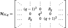 (18)
(18) Let us consider q =1/2 (we could alternatively take q =− 1/2) which makes the leading diagonal symmetric. We can then express this matrix Hamiltonian \(\widetilde {\mathcal {\boldsymbol {H}}}_{N} \equiv \boldsymbol {\mathcal {H}}_{N,q=1/2} \) in block form as
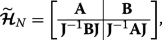 (19)
(19) where
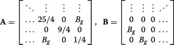 (20)
(20) are both of dimension N /2-by- N /2, and J is the exchange matrix. We may construct a matrix via permuting \(\boldsymbol {\mathcal {H}}_{N}\) with the N -by-N permutation matrix \(\boldsymbol {\mathcal {P}}_{N}\),
$$ \boldsymbol{\mathcal{P}}_{N} =\left[ \begin{array}{cccccc} 1 &0 &\hdots &\hdots &\hdots &0 \\ 0 &\hdots &\hdots &\hdots &\hdots &1 \\ 0 &1 &\hdots &\hdots &\hdots &0 \\ 0 &\hdots &\hdots &\hdots &1 &0 \\ \vdots &&&&&\vdots \\ 0 &\hdots &\hdots &1 &\hdots &0 \\ \end{array} \right], $$ (21)such that the permutation-similar matrix is
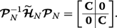 (22)
(22) Hence, the eigenvalues of \(\boldsymbol {\mathcal {P}}_{N}^{-1}\widetilde {\boldsymbol {\mathcal {H}}}_{N} \boldsymbol {\mathcal {P}}_{N}\), which are the same as the eigenvalues \(\widetilde {\boldsymbol {\mathcal {H}}}_{N}\), are double degenerate with the values given by the eigenvalue spectrum of the tridiagonal matrix C
 (23)
(23) which can also be expressed succinctly in terms of the previously defined matrices via \(\mathbf {C}=\boldsymbol {\mathcal {P}}_{N/2}^{-1}\mathbf {A}\boldsymbol {\mathcal {P}}_{N/2}+\boldsymbol {\mathcal {P}}_{N/2}^{-1}\mathbf {B}\mathbf {J}\boldsymbol {\mathcal {P}}_{N/2}^{4}\). We can see that applying C ⊥ ≠0 (inset of Fig. 3a) or both C ⊥ および A g ≠0 (inset of Fig. 3b) ruins the symmetry in the matrix Hamiltonian and prevents the existence of eigenvalues with multiplicity beyond unity, resulting in the appearance of band gaps.
Energy crossing at centre of Brillouin zone between third and forth subbands
As an example, let us specifically consider the case where p =2, wherein the matrices (12) and (13) become:
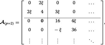 (24)
(24) and
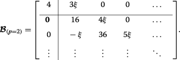 (25)
(25) This case corresponds to the crossings of the blue curves at the edge of the Brillouin zone in Fig. 3d (whereas p =0 results in crossings at q =0 in Fig. 3b). The lower eigenvalues are found exactly by diagonalizing each of the two finite matrices and they interlace, yielding \(\eta _{0,1,2} =2-\sqrt {4+4\xi ^{2}}, 4, 2+\sqrt {4+4\xi ^{2}}\). The infinite lower-right-hand block tridiagonal matrices coincide, thus the remaining double degenerate eigenvalues are found by approximately or numerically solving Det[D −η I ]=0.
データと資料の可用性
The data for the figures all stem from numerically diagonalizing the matrix described by Eq. 5 and can readily be achieved in any numerical software package. With this in mind, the datasets used and/or analyzed during the current study are available from the corresponding author on reasonable request.
ナノマテリアル