


多層プール – PCB 層を理解するための最も包括的なガイド
多層プールでは、プリント基板にはさまざまな層があります。レイヤーは、ニッチに完全に熱心で精通していない人を混乱させる可能性があります.
迅速に作成された PCB プロトタイプのほとんどは 2 層です。しかし、多くの電子機器は二層基板に限定されません。より高くて細かいボードが必要です。
この記事は、PCB レイヤーとその機能について理解を深めるのに役立ちます。
PCB レイヤーとは
1.1 PCB レイヤーの定義
プリント基板は、中継するメッセージによって意味が異なります。 PCB 層については、特定の数量と順序で指定された銅層としても記述してください。
銅層は、信号層または単に層と呼ぶことができます。 PCB 層は、その配置と提供する機能にちなんで名付けられています。銅層の数に応じた PCB のランク。
たとえば、1 層または 2 層の基板は、それぞれ 1 層 PCB または片面 PCB および 2 面層 PCB または単に両面 PCB と呼ぶことができます。
PCB レイヤーにはさまざまなタイプがあり、一般的なものは次のとおりです。
1.メカニカルレイヤー
2.オーバーレイ/シルクスクリーンレイヤー
3.ルーティングレイヤー
4.ソルダーマスクレイヤー
5.はんだペースト層
6.レイヤーを入れない
7. グランド プレーンと電源プレーン
8. 飛行機の分割
すべての PCB が上に挙げたすべての層で構成されているわけではないことに注意してください。デザインの詳細によって、さまざまなレイヤー タイプの必要性が決まります。単層ボードは通常、6 層タイプで構成されます。
これらには、メカニカル、キープ アウト、配線、オーバーレイ、はんだマスク、はんだペースト層が含まれます。
多層 PCB に関して言えば、それらは 6 つの層に加えて、他の電源装置、グランド プレーン、および追加の配線層の組み合わせで構成されます。
2 層、4 層、および 6 層の PCB が最も一般的な基板であり、12 層を超える PCB も珍しくありません。
1.2 メカニカル レイヤー
複数のメカニカル レイヤーを使用することもできますが、ボードを作成するには少なくとも 1 つ必要です。最も基本的なメカニカル レイヤーは、ボードの物理的な寸法を定義します。
メカニカル レイヤーは、メカニカル 1 とも呼ばれます。製造者が材料から回路基板を切り取る際に使用するレイヤーです。
プリント回路基板は、基板の物理的寸法を概説する単一の配線層のように単純な場合もあれば、この記事で言及されているすべての層を含む多くの層を持つ基板のように複雑な場合もあります.
一方、個別に考えると、すべての単一の層には特定の機能しかありません。各層の目的を理解することは不可欠です。なぜなら、それを理解した瞬間に、基板がどれほど複雑であっても、PCB の構築は非常に単純になるからです。
このフレームワークは、単純な長方形でも、曲線の角と切り欠きのある複雑な形状でもかまいません。
これはめったにありませんが、より多くの機械的なレイヤーが含まれており、ツールの仕様と追加のその他の自動情報が指定されています。ただし、これらの追加の機械層は、ほとんどのプリント回路基板では必要ありません。
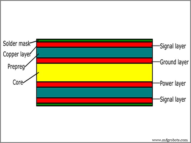
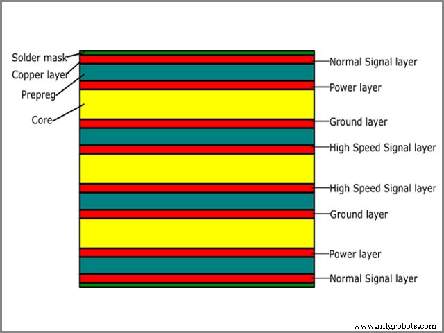
レイヤー スタック アップ (PCB レイヤーと区別)
2.1 レイヤースタックアップとは?
レイヤースタックアップは、レイヤータイプの適切な配置です。 PCB は一般に 3 つに分類されます。
- 単層。
- 二層。
- 多層。
上記の用語は、PCB の銅層の数を表しています。多層 PCB は、4、6、および 8 の範囲で 2 つ以上の層を持つものを表します。
多層では、最上層と最下層は外層と呼ばれ、中間層は内層と呼ばれます。多層 PCB の製造は複雑なため、2 層や単層の PCB に比べて非常にコストがかかります。
レイヤー スタックアップでは、考慮できることがいくつかあります。これらには次のようなものがあります。
- 下地の素材
- PCB 層の順序
- 銅の厚さ
回路の設計が異なれば、それらに適切に適合する層のスタックアップも異なります。層の積み重ねは、プリント回路基板の機能に不可欠です。
レイヤ スタックアップが適切に計画されていない場合、次のようなさまざまな問題が発生する可能性があります。
- シグナルのクロストーク。
- カップリング。
- 行き過ぎ。
- アンダーシュート。
- 電磁干渉。
- シグナル散逸。
上記の問題やさらに多くの問題を回避するには、よく計画された PCB 層を積み重ねることが不可欠です。効率的な PCB レイヤー スタックアップを設計することで、大幅に節約できます。これにより、不適切な設計によって発生する可能性のある問題を防ぐことができます。
PCB レイヤー順序以外のレイヤー スタックアップでは、基板材料、銅の厚さも考慮されます。
さまざまな種類の回路設計に対応するさまざまなレイヤー スタックがあります。よく計画された PCB レイヤー スタックは、電磁干渉、信号のクロストーク、カップリング、オーバーシュートとアンダーシュート、および信号損失の減少など、PCB の最高のパフォーマンスを保証します。
設計を完了し、初めて認定を受けることで、コストと設計サイクル時間を大幅に削減できます。シグナル インテグリティの問題が発生する前に解決できれば可能です。
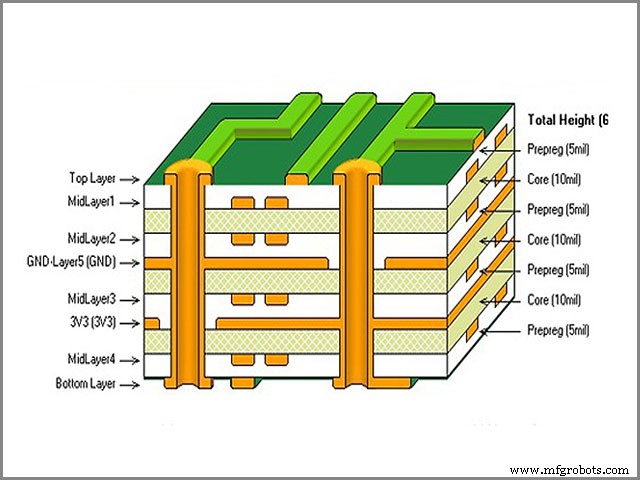
2 つの 8 層の下の図 1 では、層の順序の変化を強調するスタック アップ スキームが示されています。
信号層以外に、電源プレーンも製品開発の成功に重要な役割を果たします。
デジタルまたはアナログの信号は、マイクロストリップ ラインまたはストリップ ラインを介してルーティングできます。これにより、クロストークが減少し、結果としてシグナル インテグリティが向上します。
低周波信号は内層にルーティングされ、高周波信号は外層にルーティングされます。
各信号層に隣接してグランド プレーン層を配置することをお勧めします。ただし、層のスタックアップと製造コストを削減するために、グランド層は 2 つの信号層ごとに配置されます。電源プレーンは、密結合を形成するグランド プレーンにも隣接する必要があります。
複数の電源レールの場合、電源プレーンは複数の部分に分割されます。通常、PCB の厚さは 1.6mm ですが、12 層以上で 1.6mm の厚さを維持するのは困難です。
2 つの 8 層の下の図 1 では、層の順序の変化を強調するスタック アップ スキームが示されています。
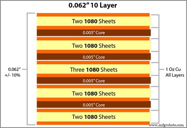
図 2 では、10 層 PCB スタックアップ スキームが説明されています。
2.2 PCB レイヤーとレイヤー スタック アップの区別
これら 2 つの用語は同じことを意味するように見えるかもしれませんが、これはまったく当てはまりません。上で定義したように、レイヤー スタック アップは、レイヤー タイプの適切な配置です。
一方、PCB 層は、特定の量と順序で与えられた銅層を指します。層のスタックアップが層の計画に関係しているのに対し、PCB 層は層の量と順序に関係しています。
PCB 層の種類
3.1 1 層 PCB
多くの場合、単層 PCB と呼ばれる単層 PCB は片面から印刷されます。これは、PCB シートの片面に導電性材料があり、もう片面に電子部品が接続されていることを意味します。
当初はすべて手作業で設計していましたが、技術の進歩によりイーグルPCBソフトなどの専用ソフトで作成できるようになりました。これは、このプログラムを搭載したコンピューターを使用して行われます。
単層 PCB にはさまざまなタイプがあります。それらのいくつかは次のとおりです:
• フレキシブル PCB。これらの単層 PCB は、硬い素材ではなく柔軟な素材でできています。この場合に使用できる材料には、プラスチックが含まれます。このタイプの単層 PCB の製造コストは非常に高く、経済的ではありません。
• リジッド PCB。これらの単層 PCB は、ガラス繊維などの硬質材料でできています。それらは柔軟性がないため、回路を曲げることができません。これらは、電卓、電源などのほとんどのデバイスで一般的に使用されています。
• 高周波 PCB。これらの単層 PCB は、動作に非常に高い周波数を必要とする回路で使用されます。このような PCB に使用する適切な材料を選択する際には、熱膨張、吸水、および誘電損失が考慮される要素の一部です
• リジッドフレックス PCB。これらの単層 PCB は、プラスチックとグラスファイバーの組み合わせでできています。 2 つの材料は両方とも 1 つの層に結合されます。この組み合わせにより、結果として PCB のサイズと重量が削減されます。
• アルミニウムで裏打ちされた PCB。これらの単層 PCB はアルミニウム材料でできています。この PCB の設計は銅製のものとほとんど同じですが、違いは使用されている記事にあるだけです。
ご覧のとおり、レイヤ PCB は非常に単純です。ただし、その単純さから、達成できることに騙されてはいけません。それらは単純かもしれませんが、複雑なデバイスでの作業に関して多くを生み出します。それらが実行するいくつかの機能があり、その中には次のようなものがあります:
- 1. ラジオおよびステレオ機器の回路で使用されます。
- 2. デジタル カメラで使用されます。
- 3. コピー機やプリンターで使用されている
- 4. デジタル計算機で使用されます。
- 5. 自動販売機で使用されます。
単層 PCB には、たとえばいくつかの利点があります。
- 思いつきやすく、デザインしやすい
- 簡単にインストールできます。
- 費用対効果が高い。
- わかりやすい。
- 短絡の可能性は低いです。
- 信頼性と効率が向上します。
3.2 2 層 PCB
2 層 PCB は、2 層または両面 PCB とも呼ばれます。主にFR-4ガラスエポキシ基板の両面に薄い銅膜または層をラミネートしたものです。これは、設計が最も簡単で最も経済的な PCB です。
2 層 PCB は、プロの PCB プロトタイピング工場 (wellpcb.com など) で簡単に製造でき、自宅で作成できます。 2 層 PCB には、上部と下部の銅層のみがあります。
経済性もさることながら、思いつく限りのシンプルなデザインです。この PCB 設計は、適切なソフトウェアを使用して自宅で簡単に製造できます。ほとんどの場合、PCB プロトタイピング会社によって作成されています。
この設計の PCB 層は、主に最上層を形成する信号層と、電気部品で構成される最下層です。 2 層 PCB のすべてのコンポーネントは次のとおりです。
- トレース
- パッド
- シルク層、上層、下層を含む PCB 層
- はんだマスク。
2 層 PCB が使用されている場所がいくつかあります。応用分野には次のようなものがあります:
• 照明中。 2 層 PCB は LED ライトで使用されているため、LED ライトに電力が供給されます。
• 医療機器。二層 PCB は、ペースメーカーや CAT チェック マシンなどの医療機器で利用されています。
• 自動車および航空宇宙産業。自動車産業と航空産業の両方で、PCB は重要な用途に使用されています。より正確には、両面 PCB は主にこれら 2 つの業界で使用されています。
2 層 PCB にはさまざまな利点があります。以下でそれらのいくつかを見てみましょう:
- 線路の敷設が簡単になります。
- セグメントの厚みを大きくすることを許可します。
- 拡張された暖かさの散乱を提供します。
3.3 4 層 PCB
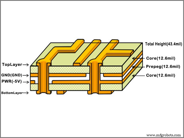
4 層 PCB には 4 つの銅層があります。最上層と最下層は配線層で、その間に挟まれた 2 つの層は電源プレーンとグランド プレーンです。
4 層の PCB 銅層の間には、コアとプリプレグがあります。製造中、これらすべての要素は、スタックアップ全体が確実に保持されるように、高熱と圧力の下でラミネートによって結合 (サンドイッチ) されます。
4 層 PCB には、スルー ビア、ブラインド ビア、埋め込みビアを含めることができます。 4 層 PCB の場合、埋め込みビアは 2 番目と 3 番目の層の間にのみ配置でき、ブラインド ビアは最上層 (1 番目) と 2 番目の層の間、または最下部 (4 番目) と 3 番目の層の間に配置できます。
4 層ボードの典型的なスタックアップは、内側の 2 層の電源とグランド、そして外側の 2 層の信号です。通常、2 つの信号層を垂直に配線します。
レイヤーが電源とグランドで分離されている場合はそれほど重要ではありませんが、隣接するレイヤーに信号がある場合は、クロストークを最小限に抑えることがより重要になります.
番号付けに関しては、通常、上から下に向かって 1 から n までです。これが唯一の規則です。本番用にファイルを送信するときにスタックアップ情報を提供するため、好きなことを行うことができます。
4 層 PCB の製造では、製造工場がある場合、コストは非常に役立ちます。
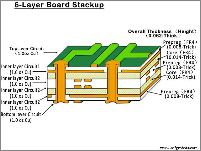
3.4 6 層 PCB
6 層 PCB を作る設計は、免疫があり、静かです。 6 層 PCB が他のものと比較して有利である理由はいくつかあります。アイデアには次のようなものがあります:
• 3 番目と 1 番目のレイヤーの間にあるトレースは、特別な処理を必要としません。
• すべてのトレースは地面に近接しています。
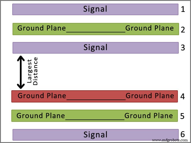
3.4.1 基準面
基準面は、リターン電流を伝達するために使用されます。 4 層の設計では、1 層目は 2 層目に高頻度のリターン通貨があり、4 層目も 3 層目に高頻度の通貨があります。したがって、6 層 PCB との違いはありません。
基準面が配線層または信号層の近くに移動すると、放射エミッションを決定するループ領域が切り取られます。 高周波での感受性。
以下は、6 層スタックがうまく機能する要因の一部です。
1. すべてのトレースによる地面への近接。
2. プランナーの静電容量を生成するグランド プレーンと電源の近接。
3. 特別な処理を必要としない第 3 層と第 1 層の間のトレース。
4. レイヤー 4 の基準面は、それとレイヤー 2 の間の距離よりも高くなっています。
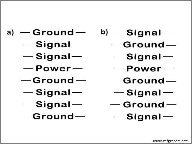
3.4.2 一般的な 6 層 PCB スタックアップ設計
最良の 6 層 PCB 設計では、PCB にある 2 つのグランド プレーンを接続するためにスティッチングが必要になります。これは、電流を基準プレーンに戻すことになっています。グラウンドプレーンを追加すると、エミッションとイミュニティに対するシールドに役立つと言う人もいます.
3.4.3 PCB プレーン カットが EMC を殺す
プレーン カットは、放射と感受性の両方で EMC に壊滅的な影響を与える可能性があります。プレーン カットまたはボイドは、電源プレーンまたはグランド プレーンがプレーンの特定の部分を意図的または意図的にカットした場合に発生します。プレーン カットにはさまざまなサイズと形状があります。
プレーン上の電流リターン パスは数千インチ離れており、適切な設計では、トレースがプレーンに隣接して走っているため、リターン電流パスが近くにあるため、ループ領域が比較的小さく形成されます。
銅プレーン層にボイドを導入する場合、ボイドとプレーン カットを横切るトレースに必要なループを作成する必要があります。これにより、現在のループ領域がより重要になります。
3.5 8 層 PCB
8 層ボードでは、配線層を 2 つ追加するか、プレーンを 2 つ追加して EMC 性能を向上させることができます。
6 層基板に対する 8 層基板のコストの増加率は、4 層から 6 層に移行する場合の増加率よりも小さいため、EMC 性能を改善するためのコスト増加を正当化することが容易になります。
したがって、ほとんどの 8 層基板は 4 つの配線層と 4 つのプレーンで構成されています。
一般に、8 層 PCB を作成するには、銅層、プリプレグ、およびコアの交互の層が必要です。プリプレグは、8 層 PCB スタックアップを 1 つのボードにしっかりと結合する接着剤として機能します。
電磁両立性を改善するためのルールに従うと、単純な 8 層 PCB 構成は次のようになります。 8 層 PCB は高いシグナル インテグリティを達成できることに注意することが重要です。 6 層 PCB 以下と比較。
信号ネットワークの数、デバイス密度、PIN 密度、信号周波数、基板サイズに応じて、PCB スタックアップ設計方法を選択できます。信号ネットワークの数が多いほど、デバイス密度が高くなります。 PIN 密度が高いほど、シグナルが高くなります。
さらに、優れた EMI 性能を得るには、各信号層にその基準があることを確認するのが最善です。
8 層 PCB を使用すると、いくつかの利点が得られます。長所と利点には次のようなものがあります:
• 中断につながる可能性のある電磁干渉を低減します。
• シグナル インテグリティが向上します。
3.6 多層 PCB
3.6.1 32 層 PCB
これは、32 層で構成された単なる多層 PCB です。レイヤーは 1 つの PCB として機能するようにまとめられます。これらの PCB 層は高度であるため、スキルと精度を考え出す必要があります。
PCB のすべての設計はソフトウェアから始まります。 32 層 PCB の場合、多くの PCB 層を含むスタックアップが作成されます。層を一緒に挟む機械を使用することで可能になります。
32 層 PCB の使用を選択できる理由については、いくつかの理由があります。アイデアには次のようなものがあります:
• 航空宇宙システムで使用されます。
• 自動車分野で使用されます。
32 層 PCB の背後にある技術
32 層 PCB を製造するには、複数の PCB 層で構成されるスタックアップが構築されます。
これは、2 層 PCB ごとに 2 層の PCB の間に絶縁繊維 - エポキシ層を介して、さまざまな 2 層 PCB を挟み込むことで可能になります。この絶縁材料はプリプレグとも呼ばれます。
これは、多層 PCB の基本構成要素が 2 層 PCB であることを意味します。
この両面 PCB 製造技術が手元にあり、複雑さの増大に対処するためのより高度な機械があれば、32 層または 50 層 PCB の製造も十分に達成できます。
32 層 PCB アプリケーション
なぜこれらの 32 層または 50 層の PCB が必要なのですか?明らかな理由の 1 つは、必要なすべてのシステム エレクトロニクスを 1 つの小型 PCB に効率的に組み込むことです。
コンポーネント アセンブリは最上層と最下層専用ですが、スタックアップの間にコンポーネントを配置することは可能です。航空宇宙産業は、これらの複雑な PCB 設計を行う上で優れた仕事をしています。
どのような航空宇宙システムでも、目標は電磁放射をできるだけ少なくするか、まったくなくすことです。設計段階で PCB を整理すると、これらの放出を抑えるのに非常に役立ちます。
各 PCB レイヤーは通常、他のレイヤーと競合しない特定の機能専用です。たとえば、中間層を電源プレーンとして使用し、最上層と最下層をコンポーネント配置用に確保することができます。
3.6.2 多層 PCB
多層 PCB には、無制限の数の導電層があります。次に、絶縁層の助けを借りて層を分離します。それらは通常、両面ボードの内側で構成されています。外層は通常、片面ボードで構成されています。
多層PCBのメーカーは、熱と圧力を利用して各PCB層を接合し、1つのPCBボードを形成します。 2 層以上の PCB は、多層 PCB として分類できます。
Its stack-up must be made as that the complete board shall meet the electrical signal and power needs and meet the mechanical strength requirements. Most professional PCB designs can exhibit around 15dB fewer emissions.
There are some reasons why you should consider using a multilayer PCB over the single or double-sided PCB’s. Some of these reasons include the following:
- They result in high quality and reliable products.
- They have a higher density of assembly.
- Increases functionality.
Precautions
When making a multilayer PCB, you must plan the configuration of your PCB stack-up. Wrong PCB configuration may give rise to undesired electromagnetic interference and poor signal integrity.
Below are some of the essential things to consider about signal when making a multilayer PCB design.
- Consider the type of signals to be routed, e.g., different signal frequencies
- Consider the signal rise and fall
- Sufficient return for the signal loop
Likely signal delay caused by permittivity – Possible cross-connection and overlap
Multilayer Pool
A circuit that has more than two layers is known as a multilayer PCB. Therefore ,this implies that the minimum number of PCB layers present for a multilayer PCB is three. Laminating the materials together is not easy but is necessary for a multilayer pool.
A multilayer pool should have no air that is trapped in between. In the manufacture of the multilayer pool, the Eagle PCB design software is necessary.
The process is complicated and, as usual, starts with the preparation of a schematic diagram. The schematic is then edited by the use of the editor menu that is on the Eagle software.
You may wonder why most PCB layers are even. It is important to note that it is more cost-effective to prepare even layers than odd ones. This is, therefore, the contributing reason for the layers being even.
4.1 Multilayer PCBs
In making multilayer PCBs, both the core and prepreg materials are used in making the layers. Prepreg materials are those that are not cured, meaning that they are malleable.
Alternative materials of both prepreg and core are then laminated together under high temperatures and pressure, making the prepreg materially, and the layers are joined together after cooling off and results in a hard and solid multilayer board.
Notice that the multilayer PCB comes with a wide range of advantages that includes:
- Increased flexibility
- Higher assembly density
- Controlled impedance features
- Small in size
- Have an EMI shielding
- It eliminates the need to interconnect harnesses which reduces the overall weight
4.2 Multilayer Pool Process
Multiple PCB making process involves using Eagle software in designing PCBs. It is a complicated procedure that starts with completing a Schematic diagram. The schematic is edited through the editor menu through Eagle software.
4.3 Multilayer Pool
After designing and drawing the schematic diagram, the next thing that needs to be done is to work out on the layout; This could be done by bringing the dimension of your printed circuit board and uploading it onto a software.
If you are using the Eagle software, you will have the opportunity to choose an appropriate grid to help each PCB layer 重なります。 This could be done using a button that routes each of the layers separately as per your needs.
Alternatively, you can make the multilayer pool for the PCB by auto-creating it using the Eagle software. However, if you choose this technique, it will be necessary that you cross check the components, text, layers, and dimensions.
You should then use the check rule option to evaluate the final layout.
4.4 Multilayer Circuit Boards
Multilayer printed circuit boards have become the core of the world’s electronics. They are the essential functions of components and wiring; This has made the new PCBs more advanced and sophisticated.
It gives the final users advanced flexible options and oddly shaped varieties to choose it. PCBs for simple electronics consist of a single layer, while sophisticated PCBs such as those used in computer motherboards are multiple layers; this is why they are called multilayer PCBs.
It is important to note that the advanced technology has allowed manufacturers to downsize PCBs significantly.
Multilayer PCBs are PCBs made with at least three copper foil layers. They appear like several single or double-sided PCBs which are glued together with heat and protective insulation. The two layers are customarily placed on the surface side of the PCB.
Electrical connections in the layers are achieved through vias like buried vias and plating through the holes; This results in a generation of complex PCBs that you will get on the market, which comes in varying sizes.
Multilayer PCBs were discovered through changes that were taking place in the world of electronics. Their continued use and function in the modern world of electronics have made them more complex and sophisticated.
Initially, PCBs had their problems, including crosstalk, capacitance, and noise. As a result, it was necessary that manufacturers had to come up with specific constraints to limit the issues.
The design consideration meant that it was prudent to design PCBs that would result in high levels of performance hence the double-sided PCB and so forth. It is this understanding that resulted in the discovery of multilayer PCBs.
It allowed for the packing of multilayer PCBs into small sizes to accommodate the ever-increasing needs of electronics.
The modern PCBs have various layers that range from 4-12 layers. The sheets come in even numbers to reduce issues such as warping, which is associated with an odd number of layers.
Also, it is cost-effective to produce an even number of layers compared to building a different number of layers.
Moreover, most modern devices that include smartphones and mobile devices use PCBs with 12 sheets. Some manufacturers can manufacture PCBs with about 32 layers.
Notice that while it is labor-intensive and expensive to manufacture multilayer PCBs, they are becoming important in the modern world.
The reason for this is that they come with a host of benefits than what you would get with double or single-layer PCBs.
4.5 Advantages of Multilayer PCBs
They are small in size; this is the most excellent feature of multilayer PCBs. They are smaller than single or double-layer PCBs, resulting in a significant benefit to the current trends.
They are more compact, robust and find much application in laptops, smartphones, and tablets. Are lightweight in construction.
The smaller PCBs are less weighty since they don’t use multiple connectors that require them to be interlinked to double-layered and single PCBs. This increases the mobility of the devices in which applied.
• High quality. Creating a multilayer PCB requires proper planning and organization, meaning that the result will be products, which are better in quality compared to the double or single layer PCBs. Also, these PCBs are more reliable.
• Increased durability. Multi-layer PCBs are durable. They can withstand much weight and can handle heat and pressure that is always applied to them during binding. They also have multiple layers of insulation material between the individual layers and a prepreg bonding agent that increases their durability.
• Highly flexible.PCB assemblers that use flexible construction techniques end up with flexible multilayer PCBs, which have highly desirable features such as the ability to be applied in areas where flexing and bending will be required. However, it is important to note that the more the layers used in a PCB, the less flexible it is.
• More powerful. The multilayer PCBs incorporate many layers into a unit PCB. So they enable the board to be more connective giving them properties that allow them to achieve higher speed and capacity even though they are small-sized.
• Single connection point. The multilayer PCBs work in a singular unit, and so they will always have just a single connection point which is not the case when you use several single or double-layered PCBs, This is of significant benefits to the electronic world as it helps to minimize the size and weight.
4.6 Disadvantages
1. Even though we have talked much about the benefits of multilayer printed circuit boards, it is critical that they come with a few problems.
2. They are costly compared to single-layer PCB because of the complicated manufacturing process and the extensive amount of time taken to construct them. This increases the labor cost which translates to high prices of PCBs.
3. They are more challenging to manufacture and require more time and advanced manufacturing techniques than single-layered PCBs because any small flaws could make them useless.
4. The supply is limited- because they need expensive machinery to manufacture, very few manufacturers can produce them, so their production is limited.
5. Require extensive design and interconnection between the layers, and one should be able to mitigate impedance issues and crosstalk. Any single mistake can lead to the non-functioning of the board.
6. Manufacturing the PCB requires plenty of time and person-hours, and so it is sometimes difficult to deliver orders within the specified timeframes.
4.7 How Multilayer PCBs Compare With Single Layer PCBs
1. They are of high density and greater functionality because layering increases their capacity and speed.
2. They are small-sized since the addition of layers increases their surface area meaning that you will have a high ability of PCB compared to what you can get in single layer PCB.
3. They are light in weight since it requires fewer connectors and can be used in complex electrical applications.
4. The multilayer PCBs have enhanced functionality compared to single layers and have great EMI shielding, controlled impedance, and more feature despite their small size.
4.8 Application
Multilayer PCBs can be put to just any use and have become a preferred option because it can use them across all technologies.
They are found in almost all electronics, including smartphones, microwaves, and other domestic consumer equipment. They are also used in smartwatches and mobile devices because they are small and have increased functionality.
In computer electronics, they find much application in the motherboards and servers. Their space-saving feature makes it easier for them to be applied widely in the technology industry.
Multilayer PCBs are also widely applied in telecommunication devices. They are used in GPS, signal transmission as well as in satellite applications. Because they are durable, they can easily use them in towers outdoors and on mobile devices.
In industries, multilayer PCBs are quite vital because they are small in size and durable. They are therefore widely applied in industrial control and are used in running machinery in industrial applications.
The medical field has also benefited greatly from PCBs. They are found in equipment that is used in diagnosis as well as those that are used in treatment.
They are small in size lightweight, and so they can use them in heart monitors, x-ray, medical testing devices, and CAT scan equipment.
The military has also benefited a lot from multilayer PCBs. They are deployed in high-speed circuits, and so they are highly utilized in military applications. They are also used in devices that require increased movement.
The automotive industry, especially the electric car, has also significantly benefited from PCBs. They are used in GPS headlight switches and engine sensors.
They are small durable and heat-resistant, a thing that makes them entirely applicable in the automobile environment.
4.9 Multilayer Pool Technology
The technology has allowed the production of quality boards and is considered key to military, communication, and other fields that rely on multilayer PCBs.
The technology enables the manufacturers to fabricate PCBs from materials such as flex, Teflon, and polyimide, allowing them to fulfill their PCB needs.
4.10 Multilayer Pool Switch
PCBs play a vital role in manufacturing computer networking devices such as multilayer switch which provides extra function including routing capability. The switch can prioritize the packets and implement QoS differentiated services in hardware.
4.11 Multilayer Pool Ceramic Capacitor
They are popularly referred to as MLCCs and are used in building blocks in modern electronics. MLCCs make up more than 30% of the components in the hybrid circuit module.
They consist of the monolithic ceramic block with electrodes that appear on the surface end of the ceramic block that forms the contact made by having burnt in metallic layer.
Types
MLCCs come in different kinds that include those that are described as tolerance, capacitance, and dielectric, case size, and so forth. Their values vary, but the most common ones range from 10 nF to 1µF. Also, their voltage rating ranges from 16V to 100V.
As technology advances, more and more multilayer PCBs are produced. These PCBs are finding much application in both the research industry and science. Are used in security appliances, alarm systems as well as fiber optic sensors.
They are also used in weather analysis equipment and atomic accelerators. Multilayer PCBs are becoming light-weighted, compact, and save on spaces.
PCB Layers Thickness
Different PCB layers have the different thickness depending on where they will be applied. For instance:
- 11 layer boards can be of 20 by 14 dimensions unless given additional specifications.
- Six layer boards are produced on a thickness of 0.031, 0.040, 0.047, 0.062 and 0.125 inches.
- Both the 8 and ten layer boards can be found with the thickness of 0.062, 0.093 and 0.125 inches.
The standard pooling thickness for multilayer PCBs is 1.55mm. This standard measurement is not the actual measurement for all the multilayer PCBs but can be used as a reference in their construction.
Pcb Layers Ordering
PCB layers are arranged in orders. The process of organizing these layers can be as follows:
• Choosing the initial number of layers. Here you will select the PCB layers that will suit the need you want to achieve. If it is for home prototyping, then one or two layers can be quite useful. Four layers of PCBs are simple or rather cheap boards.
Six-layer PCBs are cheap and abundant. Eight-layer PCBs are quite cost-effective, while the 12 layers PCBs are ideal for heavy industry boards or just boards with many tracks.
• Starting the layout
• Here, you will begin with the top and bottom signal layers. Depending on the design that you are using, the two top and bottom signals would be just enough unless you have too many connections requiring inner signal layers.
There are some options that you can use to order your PCB layers. The following are some of the most common ones:
- Four layer stack up.
- Six layer stack up.
- Eight-layer stack up.
- Ten layer stack up.
- 12 layer stack up with two additional signal layers.
- 12 layer stack up with 4 GND’s.
You can make a quote of the type of PCB you would want here https://www.wellpcb.com/pcb-quote
結論
As you have seen, PCB layers make up different designs of Printed Circuit Boards for various appliances. Depending on where you would want to use the PCBs, the sheets would vary.
The single and double-sided layers are cheaper to construct but do not perform the complex operations that the multilayer PCBs can do. The multilayer PCBs are used in more advanced machines and electronics as compared to the others.
The multilayer PCBs are made out of three or more PCB layers formed of copper, among other materials. In case of any inquiries and issues, you can contact us through the following:
• www.wellpcb.com
産業技術