


自動車 PCB の特性と設計上の考慮事項
電子部品は、自動車においてますます活発な役割を果たしています。現在、トップレベルの車両には 200 を超える電子制御ユニットが搭載されており、その一部は車のコックピットに適用されるセンサーやプロセッサです。自動車用の電子製品の価値は動的システム、ボディ、シャーシにあり、その大部分はデジタル電源に関係していると結論付けることができます。
自動車における電子システムの適用は、次の 3 つの側面をカバーして、自動車の性能を向上させることを目的としています。環境改善とは、燃料の節約、テールガスの削減、ガソリン、天然ガス、バイオ燃料からハイブリッド パワーおよびピュア パワーへの燃料転換を指します。このように、電気自動車は自動車産業の戦略的方向性となっている。
b.セキュリティの強化は、エアバッグ、レーダー監視、ステレオカメラ、赤外線監視、自動回避から自動運転に至るまで、交通事故の減少にあります。現在、自動運転車は多くの注目を集めており、投資を行っています。
c.利便性と快適性は、一般的に、オーディオ、ビデオ ディスプレイ、エアコン、コンピューター、モバイル通信、インターネット、ナビゲーション、利便性と人間化を考慮した電子料金収受に根ざしています。
電子機器のバックボーンとして、自動車に適用される PCB (プリント回路基板) も上記の要件を満たす必要があります。
自動車 PCB の基本要件
• 品質保証要件
製造業者や流通業者にとっての長期的な品質保証の基本的な要求は、国際的な観点からの健全な品質管理システム、つまり ISO9001 にあります。自動車業界の特殊性から、1994 年に北米の大手自動車メーカー 3 社が共同で自動車業界独自の品質管理システム、QS9000 を確立しました。 21 st の初めに 20 世紀、ISO9001、つまり ISO/TS16949 の規制に基づいて、世界の自動車メーカーによって新しい品質管理システムが発行されました。
ISO/TS16949 は、世界中の自動車産業の技術規制として、自動車産業の特別な要件を統合し、自動車部品のサプライ チェーンにおける欠陥防止、品質変動、廃棄物削減に重点を置いています。
したがって、自動車用 PCB メーカーが自動車市場に本格的に参入する前に、最初に取得しなければならない認証は ISO/TS16949 です。
• パフォーマンスに関する基本要件
を。高い信頼性
自動車の信頼性には、主に 2 つの側面があります。1 つは、制御ユニットと電子部品が正常に動作する耐用年数であり、もう 1 つは、自動車の制御ユニットと電子部品が極端な環境で優れた動作をすることを可能にする耐環境性です。
自動車の平均耐用年数は 10 年から 12 年で、その間はコンポーネントまたは脆弱な部品のみを交換できます。言い換えれば、電子システムと PCB は、自動車と同じようにサービス年を特徴とする必要があります。
車両は、適用の過程で気候や環境の影響を受ける傾向があり、凍えるような寒さ、極端な暑さ、長期にわたる日光や雨などがあります。それらとは別に、電子部品やシステムの動作によって発生する熱によって引き起こされる環境変化に悩まされなければなりません。自動車の電子システムや PCB も同様です。自動車の電子システムは、温度、湿度、雨、酸性煙、振動、電磁干渉 (EMI)、電流サージなどの過酷な環境に打ち勝たなければなりません。
b.軽量・小型化
軽量・小型化は、各部品や回路基板の軽量化・小型化による省燃費に有利です。例えば、自動車用ECU(Electronic Control Unit)の体積は1,200cm 3 21 st の初めに 世紀は少なくとも 4 倍縮小されています。 PCB の軽量化と小型化は、密度の向上、面積の縮小、薄さと多層化に由来します。
自動車 PCB の性能特性
• 複数のタイプ
機械装置と電子装置の組み合わせとして、最新の車両技術は伝統的な技術と最新の科学技術を統合しています。さまざまな部品がさまざまな機能を持つ電子デバイスに依存しており、さまざまな使命を持つ PCB のアプリケーションにつながっています。
自動車用プリント基板の基板材料の違いから、無機セラミック系プリント基板と有機樹脂系プリント基板に分類できます。セラミックベースの PCB の主要な特性は、高い耐熱性と優れた寸法安定性であり、高熱環境のエンジン システムに適用できます。それにもかかわらず、セラミックベースの PCB は製造性が悪く、回路基板のコストが高くなります。耐熱性が向上した新開発の樹脂基板の開発により、樹脂ベースの PCB はほとんどの現代の車両に適用されています。
1 つの一般的な規則に従います。異なる性能を持つ基板材料を使用する PCB は、異なる機能の実装を担当する車両の異なるセクションに適用されます。次の表は、車両デバイスまたは計器の一部と互換性のある PCB タイプを示しています。
| 車両デバイス | PCB の種類 |
| スピードメーター;エアコン | 1 層/2 層 PCB 1 層/2 層フレキシブル PCB |
| カーステレオ;モニター | 2 層 PCB 多層 PCB フレキシブル PCB |
| 車載通信機器;ワイヤレスロケーションアプライアンス;セキュリティ管理システム | 多層 PCB HDI PCB フレキシブル PCB |
| エンジン システム;送電制御システム | メタルコア PCB リジッド フレックス PCB |
| 車両のパワー コントローラー。ナビゲーション デバイス | 組み込み PCB |
• 車両のさまざまなセクションにおける PCB の信頼性要件
自動車は公安に関わる移動手段として、信頼性の高い製品群に属します。通常の寸法、外観、機械および電子機器の性能要件とは別に、信頼性に関する一連のテストをそれらに実装する必要があります。
を。熱サイクル試験 (TCT)
車両の部位に応じて5段階のレベルが設定されています。以下の表は、車両のさまざまなセクションでの PCB の熱サイクル温度をまとめたものです:
| 車両セクション | レベル | 低温 | 高温 |
| 車体内 | A | -40°C | 85°C |
| 下の車両シャーシ | B | -40°C | 125°C |
| エンジンの上 | C | -40°C | 145°C |
| トランスミッションパーツ | D | -40°C | 155°C |
| エンジン内 | え | -40°C | 165°C |
b.熱衝撃試験 (TST)
自動車用 PCB が極度の熱環境に適用されるのはごく普通のことです。重い銅 PCB は、外部からの熱とそれ自身の身体から生じる熱の両方に悩まされなければならないため、特に困難です。このため、自動車用 PCB の耐熱性に対する要求はさらに高くなります。
熱衝撃試験に参加するには、自動車用 PCB を 260°C または 288°C の高温のはんだペーストに 10 秒間 3 回浸漬する必要があります。 .現在、PCB アセンブリでは鉛フリーはんだが比較的高いはんだ付け温度で使用されており、熱衝撃試験の必要性が高まっています。
c.温度湿度バイアス (THB) テスト
自動車用 PCB は、雨の日や湿気の多い環境など、多くのダイナミックな環境を通過する必要があるため、PCB CAF (Conductive Anodic Filament) の可動性も検査できる THB テストを実行する必要があります。 CAF は、回路基板上の隣接するビア間、隣接するビアとワイヤ、隣接するワイヤと隣接する層の間でのみ発生します。そのような状況での絶縁性は低下するか、近道につながることさえあります。絶縁抵抗は、ビア、ワイヤ、およびレイヤー間の距離によって決定する必要があります。
自動車用 PCB の製造機能
• 高周波 PCB
軍用レーダーと同様に、近距離レーダー、自動車の衝突防止システムまたは予測緊急ブレーキ システムは、PCB に依存してマイクロ波高周波信号を送信します。したがって、誘電損失の低い基板材料が推奨され、通常は PTFE (ポリテトラフルオロエチレン) が適用されます。基板材料としての通常のFR-4とは異なり、PTFEまたは同様の高周波材料は、当然、明確な製造可能性を必要とします。例えばビア穴あけ加工では特殊な穴あけ速度が必要です。
• 重銅 PCB
車両は、電子密度と電力が高いため、より多くの熱を発生する傾向があります。ハイブリッド パワーと完全電気自動車の数が増えるにつれて、高度な送電システムが要求され、放熱能力と大電流に対する要求が高まります。これを実現するには、PCB の銅の厚さを増やすか、銅のリードと金属を多層 PCB に埋め込む必要があります。
厚い銅の多層 PCB を製造するのは非常に困難ですが、厚い銅の 2 層 PCB を製造するのは簡単です。重要なポイントは、重い銅のグラフィック エッチングと重い銅のギャップ充填にあります。
厚銅多層 PCB の内部回路は厚銅です。その後、グラフィックスを転写するには、非常に耐食性に優れた厚手のフィルムが必要です。重い銅の優れた回路を確保するために、エッチング時間は十分に長く、エッチング装置と技術的条件は最適な状態を維持する必要があります。
内部導体と絶縁体基板材料の表面に大きな差があり、通常の多層プリント基板の積層では樹脂が完全に充填されず、キャビティが発生するため、樹脂を多く含む薄いプリプレグが提案されます。一部の多層 PCB には、異なる銅厚の内部回路が含まれているため、大きな区別と小さな区別がある領域に異なるプリプレグを使用できます。
• コンポーネントの埋め込み
組み込みコンポーネント PCB は、アセンブリ密度を高め、製品全体のサイズを縮小するために携帯電話に最初に適用されました。これは、他の電子製品にとっても本質的に重要です。そのため、車載用電子機器に組み込み技術が使用されています。
コンポーネントの埋め込み方法に基づいて、多くの埋め込み PCB 製造オプションがあります。
a.溝は最初にフライス加工され、次にSMDがウェーブはんだ付けまたは導電性ペーストによって組み立てられます。
b.
c.薄膜SMDは、最初にウェーブはんだ付けによって内部回路上に組み立てられます。
d.セラミックベースに厚膜部品を印刷する。 SMDはウェーブはんだ付けで組み立てられ、その後樹脂がパッケージングに使用されます。このタイプの組み込み PCB は、耐熱性、耐湿性、耐衝撃性などの車両の要求に、より適合し、高い信頼性を備えています。
• HDI テクノロジー
スマートフォンやタブレット PC と同様に、エンターテイメントや通信の機能に関しては、車両にも HDI PCB が求められます。その結果、マイクロビア穴あけ、電気メッキ、および相互接続技術を自動車用 PCB に適用する必要があります。
自動車 PCB 設計の考慮事項
• インダクタの向き
2 つのインダクタ (または 2 つの PCB ワイヤ) が互いに近づくと、インダクタンスが生成されます。一方の回路 (回路 A) の電流によって生成された磁場は、その後、もう一方の回路 (回路 B) の電流を駆動します。このプロセスは、変圧器の一次カラーと二次カラーの間の相互効果と似ています。 2 つの電流が磁場を介して相互作用すると、生成される電圧は相互インダクタンス (LM) によって決定されます。 ): . In this formula, YB is the error voltage input to Circuit B while LA is the current through Circuit A. LM is quite sensitive to circuit spacing, inductance loop area and loop direction.
Therefore, an optimal method to arrange all inductors in a circuit can be achieved through compact circuit layout and coupling balance reduction.
Distribution of mutual inductance is related with inductance alignment. Therefore, direction modification of Circuit B makes its current loop parallel to magnetic lines of Circuit A. To achieve that, inductors should be vertically arranged, which is beneficial to mutual inductance reduction.
Inductor layout rules for automotive PCBs:
a. Inductor space should be as large as possible;
b. Inductor alignment should be set as right angles so that crosstalk between them will be minimized.
• Lead coupling
Similar with inductor alignment affecting magnetic field coupling, if leads are close to each other, coupling will be affected as well and mutual inductance will be possibly generated. The leading issue in RF circuit lies in sensitive component layout such as input matching network, receiver's resonant channel and emitter's antenna matching network.
Return current path should be as close to main current path as possible with radiation field minimized, which is beneficial to current loop area reduction. Optimal low impedance path is normally grounding area under leads, that is, loop area is effectively limited in the area with dielectric thickness times lead length. If grounding area is split, however, loop area will be enlarged. For leads going across split area, return current will be forced to go across high impedance path, which greatly increases current loop area. This type of layout also makes circuit accessible to mutual inductance.
In a word, integrated grounding should be ensured under leads as much as possible since integrated mass area grounding is beneficial to circuit performance improvement.
• Grounding thru-hole
The main issue RF circuit has to solve usually lies in bad characteristic impedance of circuits, including electronic components and interconnection. Copper layer with low thickness is equivalent to inductance wire. Moreover, distributed capacitance can be formed by the combination between copper layer and adjacent leads. As leads go through thru holes, inductance and capacitance characteristics will be displayed as well.
Thru-hole capacitance mainly derives from capacitance between copper at thru-hole pad edge and bottom copper. Another element affecting thru-hole capacitance is cylinder of metal thru holes. Parasitic capacitance affects little since it usually just leads to low signal edge of high-speed digital signals.
The largest effect of thru holes is corresponding parasitic inductance aroused by interconnection. Because majority of metal thru holes feature the same dimension as that of integrated components in RF PCB design, this formula can be used to estimate the effect of thru hole: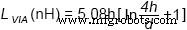 . In this formula, LVIA is the integrated inductance of thru holes; h refers to via height with inch as unit; d refers to via diameter with inch as unit.
As a result, circuit layout should conform to the following principles:
a. Inductance module should be established for thru holes in sensitive area;
b. Filter or matching network depends on independent thru holes;
c. Thinner PCB copper will reduce the effect of thru hole parasitic inductance.
• Grounding and filling
Grounding or power plane defines a public reference voltage that supplies power to all components in the system through low impedance path. Based on that scheme, all the electric fields can be balanced with excellent shielding scheme generated.
Direct current always flows through low impedance path. Similarly, high-frequency current is also a path flowing through the lowest impedance at the first minute. Therefore, for standard PCB leads above ground plane, return current tries to flow into the grounding area rightly under leads. Afterwards, split grounding area arouses all kinds of noises, which further increases crosstalk through magnetic field coupling or current accumulation. As a result, ground integrity should be ensured as much as possible, or return current will drive crosstalk.
In addition, filling ground, also called protective wire, is usually applied for design of circuits containing areas where continuous ground is difficult to be arranged or that requires shielding sensitive circuits. Grounding thru holes can be positioned at terminals of wires or along the wires to increase shielding effect. Protective wires can't be mixed with leads designed to provide return current path, which will bring forward crosstalk.
When copper area isn't connected to ground or connected to ground at one terminal, its validity will be decreased. In some cases, parasitic capacitance will be generated with ambient impedance changed or potential path formed between circuits, which, thus, lead to bad effect. Simply speaking, if copper has to be arranged on the board, the same electroplating thickness should be maintained.
In the end, grounding area near antenna has to be taken into consideration. Any monopole regards grounding area, routing and thru hole as a section of system balance and non-ideal balanced routing will affect radiation efficiency and direction of antenna. Therefore, grounding area mustn't be directly placed right under monopole antenna of a circuit board.
To sum up, the following design principles should be conformed to in terms of grounding and filling:
a. Continuous grounding area with low impedance should be provided as much as possible;
b. Two terminals of filling wires should be connected to the ground with thru hole array applied;
c. Copper-coated lines have to be connected to the ground near circuit around which copper coatings aren't necessary. When it comes to circuit boards with multiple layers, a grounding thru hole should be arranged as signal lines are transferred from one side to the other.
In conclusion, automotive PCB design rules can be summarized into the following table:
| Inductor layout | • Inductor space should be as large as possible; • Inductor alignment should be set as right angles; |
| Integrated grounding | • Integrated grounding should be arranged under leads; |
| Through holes | • Inductance module should be set for thru holes in sensitive area; • Filter or matching network depends on independent thru holes; • Thinner PCB copper reduces the effect of thru hole parasitic inductance; |
| Grounding and filling | • Continuous grounding area with low impedance should be provided; • Connect terminals of filling wires to the ground with thru hole array applied; • Copper-coated lines have to connected to the ground; |
Article wrote by PCBCart editor Dora Yang, first published on Bodo's Power System Magazine August issue, 2017.
You might also be interested in the following articles:
• Properties of Flex-Rigid PCB Used for Automotives
• 5 Tips for Automotive Circuit Design to Defeat EMI
• SMT Soldering Reliability Research Based on Circuit Module in Automotive Electronic Industry
• 5 Proven Ways to Judge Reliability of Automotive PCB Manufacturers
• How to Evaluate an Automotive HDI PCB Manufacturer
産業技術