


2D半導体ナノ材料とヘテロ構造:制御された合成と機能的応用
要約
グラフェンを超えた2次元(2D)半導体は、最も薄く安定した既知のナノ材料を表しています。 21世紀の最後の10年間に家族とアプリケーションが急速に成長したことで、高度なナノおよびオプトエレクトロニクス技術に前例のない機会がもたらされました。この記事では、開発された2Dナノマテリアルに関する調査結果の最新の進捗状況を確認します。これらの2Dナノ材料とヘテロ構造の高度な合成技術を要約し、それらの新しいアプリケーションについて説明しました。製造技術には、最先端のが含まれます 2D半導体の化学蒸着(CVD)、原子層堆積(ALD)に特に焦点を当てた、アモルファスと結晶の両方の2Dナノ材料を製造するための気相ベースの堆積法と新しいファンデルワールス(vdW)剥離アプローチの開発およびそれらのヘテロ構造、ならびに液体金属の2D表面酸化膜のvdW剥離。
はじめに
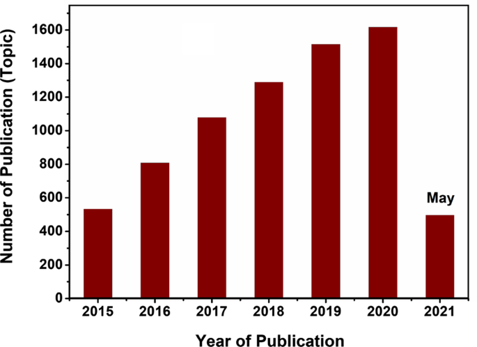
グラフェンの高貴な価格(2010年)とそれに続くグラフェンを超えた2D半導体の開発の進歩に続いて、2Dナノ材料とそのヘテロ構造に基づく材料科学の独立した科学分野の大幅な成長が21年の20年の間に目撃されました。世紀[1,2,3,4]。報告されている2Dナノ材料の構造では、電子移動とバンドギャップ変調に起因する非常に興味深い物理化学的現象が観察されています[5、6]。グラフェンにはバンドギャップがないため、半導体の特性や大きな注目を集めることができず、遷移金属ジカルコゲナイド(TMDC)、六方晶窒化ホウ素( h > -BN)、黒色閃光、遷移金属酸化物など[7,8,9,10,11,12,13,14,15,16]。グラフェンを超えたこの2Dナノ材料ファミリーは、金属から半金属、さらには半導体から絶縁体まで、幅広い特性をカバーする幅広い電子特性を示しました[17、18、19、20]。幅広い電子特性に加えて、高表面積、ダングリングボンドの欠如、表面状態の性質、卓越したスピン軌道相互作用特性、量子スピンホール効果など、2D材料の他の特性は、非常に興味深い特性を調整します。個々のナノ構造の2D材料[21、22、23、24、25]。その結果、このタイプの2Dナノ材料に対する科学界の関心は、前例のない半導体特性のために、特に過去10年間で指数関数的に増加しています。次に、この関心は、図1に示されている2D半導体(Web ofKnowledge™データベース)に特化した公開記事の比例的な指数関数的上昇に適切に反映されています。
「 2D半導体」の掲載記事数のダイナミクス 」はWebofKnowledge™に基づいています
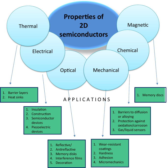
2D半導体ナノ材料の特性の初期の測定は、それらの微細構造およびバルクの対応物の特性と比較できなかった独特の電子特性を明らかにしました。これらの際立った特徴は、2D材料のナノスケールの低次元性に起因する量子閉じ込め効果に関連しています[26]。したがって、2D材料のこれらの独自の仕様は、それらの基本的な物理学と化学を研究するための優れたプラットフォームを提供します。最初に広く研究されたクラスの2Dナノ材料は、層状TMDC( XY )です。 2 、ここで X =Mo、Ti、W、 Y =S、SeおよびTe)[27,28,29,30,31,32,33,34,35,36,37,38,39]。この段階で得られた結果は、ジカルコゲニド半導体が2Dおよびバルク導電率(σ)にかなりの違いがあることを確認しました。 1 / σ 2 〜10 2 –10 3 )[40]。さらに、二硫化モリブデン(MoS 2 )などの単分子層2D材料の一部 )、は直接バンドギャップ半導体です[41]。得られた2DTMDCの電子特性は、次世代の最新のナノおよびオプトエレクトロニクスデバイスのさらなる開発に不可欠な意味を持っています。これらの発見および他の異方性は、強力な中間層 X の存在から生じます。 – Y 結合。これは、層間の弱いvdW相互作用とは対照的です[42]。たとえば、TiS 2 六角形の層状構造で結晶化し、1つの六角形に充填されたTi原子のシートが各単分子層の2つの六角形の硫黄シートの間に挟まれます[43]。原子のこの特定の層状構成は、層状2Dナノ構造のvdW層間剥離を可能にしました。その結果、以前のレポートのほとんどは、機械的およびvdW剥離技術によって合成された2D材料の特性に焦点を当てていました。 2Dフィルムは非常に薄いため、透明、軽量、柔軟性があり、非常に興味深い特性を備えています。これらのユニークな機能は、バッテリー、スーパーキャパシター、燃料電池などのエネルギー貯蔵および変換アプリケーションを備えた高性能電極材料の開発への道を開きました[44]。たとえば、図2は、典型的なアプリケーションで利用された2D半導体とヘテロ構造の主な特性をまとめたものです。
典型的なアプリケーションで利用される2D半導体の特性
注目すべきことに、2Dナノ構造半導体の分野は、ナノファブリケーションの最新の技術的進歩により、最新の高性能ナノおよびオプトエレクトロニクス機器の開発のための重要な知識として独立して立ち上がっています[45]。 2Dナノ材料の原子スケールの層状構造は、それらの優れた特性の起源であり、材料特性の正確な調整可能性は、それらの寸法の原子レベルの制御によって提供されます。したがって、均一な厚さの超薄膜のコンフォーマル合成は、2Dナノ材料に基づく高度な電子機器の製造方法の開発に向けた基本的なステップとして非常に望ましい。具体的には、所望の基板上に正確で均一な厚さのウェーハスケールの超薄膜を製造するために、2D半導体に基づく機器の製造のための成功した合成技術を開発する必要があります[46]。さらに、合成および製造段階で、2Dナノ材料を装飾することができ、導電体、絶縁体、さまざまな幾何学的特徴を備えた基板など、電子ユニットのさまざまなコンポーネントと直接接触する可能性があります。また、2Dナノマテリアルと他のコンポーネント間のヘテロ界面がそれらの特性に根本的に影響を与える可能性があることも考慮に入れる必要があります。これは特に2D層間の電荷移動メカニズムに関連しています[47]。ヘテロ構造の2Dフィルムの独自の機能により、ヘテロ構造の電子機器、オプトエレクトロニクス、バイオセンシング、環境センサー、触媒作用、ウェアラブルおよびフレキシブルエレクトロニクス、メモリスタ、シナプスデバイスなどの多くのアプリケーションで使用できます[36、44、48 、49、50、51、52、53、54、55]。したがって、合成および製造技術は、2Dナノ材料に基づく機能的機器の製造の複雑さに対応する必要があります。さらに、2D材料の電子特性は、物理的および化学的構造、寸法、層数、形態、配向、構造相、ドーピング欠陥、アモルファス性または結晶性、およびそれらの構造の粒界などの材料特性に大きく影響されます。 [56]。 2Dナノ構造の層の数は、電子構造に追加の基本的な影響を及ぼし、2D材料の特性が、2Dフィルムに基づく電子デバイスの最終的な性能を完全に決定します[57]。
一方、2D材料の結晶化度またはアモルファス性も、それらの電子特性を変化させる可能性があります。合成方法とその条件によって決定される2Dナノ材料は、欠陥がないことができます。 (単結晶)またはいくつかの不純物レベルまたはいくつかの粒界を含みます。したがって、界面散乱現象による電荷移動度は、粒界の数によって影響を受けます[58]。単結晶構造は最高の電荷移動度と低い界面散乱を持っていますが、アモルファス2D構造は最高の絶縁特性を表しています[58]。 2Dナノ材料の初期の合成方法のほとんどは、2Dナノ構造の機械的剥離に基づいていました。層状構造間のvdW力が弱いため、機械的および化学的剥離を効果的に使用して、層状2Dナノ構造を抽出できます[59]。したがって、機械的剥離により、高品質の結晶性2D構造がホスト材料から分離されます。しかし、機械的剥離はすでに大規模な2Dナノフィルムの合成に失敗しています。同様に、2D材料の液相剥離は、2D材料の低コストで大規模な生産に適したもう1つのアプローチです。それにもかかわらず、品質管理とサイズの均一性は、この剥離技術を介した2Dフィルムの合成の主な課題です[58]。それどころか、蒸気ベースの堆積技術による2D膜の直接成長は、正確な寸法制御を備えた高品質のウェーハスケールの2Dナノフィルムを製造するための最も信頼性が高く適用可能な合成方法の1つであることがわかりました。たとえば、CVDとALDは、ナノ構造の2D半導体とそのヘテロ構造の大面積製造に際立った技術的利点を提供する2つの主要な蒸着技術です[60、61]。厚さ、化学組成、結晶化度状態、さらにはドーピング元素と構造欠陥の割合の正確な制御は、それぞれCVDプロセスとALDプロセスの成長パラメータを注意深く操作することで適切に達成できます。さらに、2Dフィルムの従来の合成方法とは別に、2D材料の他の新しいソースがほんの数年前に登場しました。たとえば、液体金属の表面酸化物は、実際には、液体合金の物理的および化学的特性から生じる前例のない特性を備えた高品質の天然2Dナノフィルムのユニークな供給源です[61]。
したがって、レビューでは、ALDおよびCVD技術に焦点を当て、液体金属の2D表面酸化物のvdW剥離に焦点を当てることにより、2Dナノマテリアルの新しい合成方法に関する最新の調査結果について説明します。気相堆積技術における2D材料の成長メカニズムについて説明し、2Dベースの半導体材料の製造と堆積における主要な課題と機会についても説明します。さらに、最近開発された液体金属の2D天然表面酸化膜のvdW剥離技術が紹介されています。最後に、最先端の 電子的および光電子的特性を含む超薄型2Dベースのデバイスの開発された機能的アプリケーションが提示され、詳細に特徴付けられています。
蒸気ベースの製造技術によって合成された2Dナノマテリアル
2D半導体材料の分野で行われている研究の主な焦点は、2Dナノ構造の合成とその後の特性評価です。これらの2Dナノ構造は、原子的で薄い厚さの無機、有機、高分子材料の広い範囲に属しています。合成戦略は通常、2つの主要なアプローチ、つまりトップダウンに従います。 およびボトムアップ 戦略。したがって、制御されたアーキテクチャと物理的および化学的特性を備えた2D半導体の開発は、さまざまなアプリケーションで重要な役割を果たし、今日の商用半導体技術よりも大幅に高いレベルに新しい可能性を開きます。それにもかかわらず、過去数年間の2D半導体における多大な努力と独自の科学的発見にもかかわらず、それらのほとんどは、産業用途では使用できない非常に単純な剥離技術を使用して実験室で得られました。 1つの選択肢は、トップダウンを表します 通常、層状材料と層状共有結合性有機フレームワーク(COF)の層間剥離とvdW剥離を伴う方法。ただし、この方法のボトルネックは、製品の収率が非常に低く、凝固中にシートが再スタックすることです。別の代替案は、ボトムアップに基づいています 2D方式での無機、有機、または高分子前駆体の異方性アセンブリ。 2Dナノ材料の製造にはある程度の成功がありますが、電気化学的エネルギー貯蔵と変換におけるさまざまな機能を備えた合理的に設計された2Dナノシートの詳細な調査は未だ原始的です。それにより、さまざまな用途でイオン拡散と電子輸送を加速するために、調整された厚さ、高表面積、優れた導電性、および機械的柔軟性を備えた2Dナノ材料の独自性の完全な調査が強く求められます。次のセクションでは、2D材料の2つの主要な堆積技術、つまり、過去数年間の成果に焦点を当てたCVDとALDの基本について概説します。
2Dナノ構造のCVD
超薄膜の気相ベースの直接成長は、超精密な寸法仕様を備えた高品質の膜を堆積するための最も信頼性が高く、適用可能な合成方法の1つです[62]。さまざまな方法の中で、CVDは、いくつかの異なる基板上に超薄膜を成長させるための最初のよく知られた成功した技術です。 CVDは、高品質の大面積2D膜を成長させるためのスケーラブルで制御可能なアプローチを提供します[63]。 CVD法を2Dナノ材料の制御可能な堆積のための信頼できる技術にするいくつかの顕著な仕様があります。この方法は、基板の表面上で蒸気状態のガス状物質を段階的に反応させることに基づいています。 CVD反応に続いて、原子層の厚さが少ない固体薄膜が成長します。したがって、2Dナノ材料の特性は、界面特性、基板の幾何学的特徴、および固体膜の構造相に大きく依存します。これらの特性は、CVD成長パラメータを正確に調整することで注意深く調整できます。 CVD成長の一般的なメカニズムを理解するには、温度、圧力、基板、前駆体などのCVDパラメータが、表面の物質移動、熱伝達、および界面反応にどのように影響するかを理解する必要があります。この点で、プロセス中の主な堆積パラメータを制御する適切に設計されたレシピを開発する必要があります[64]。さらに、2Dナノフィルムのドーピングレベルを制御することができます。これは、特定の特性を備えた半導体ナノ構造の設計に不可欠な機能です[64]。たとえば、CVDプロセス中にカルコゲンと金属の空孔のレベルを制御することが可能です。以下のCVDプロセスの重要なパラメータは、構造相、形態、および界面反応に大きく依存します。
温度
温度は、前駆体の化学反応速度、キャリアガスの流量、そして最後にCVD膜の成長速度に影響を与えるなど、CVD膜の成長中に相互に関連するいくつかの要因に直接影響する主要な基本パラメータの1つです[64]。一般に、CVD温度が高いと、高品質の2DCVD膜が確実に堆積します。ただし、極端に高温になると欠点もあります。具体的には、高濃度のグラジエントを生成する可能性があるため、システム内で不安定な質量流量と移動を引き起こします[64]。また、チャンバー内のコンポーネントの飽和圧力に直接影響し、その結果、薄膜の成長速度を変化させます。温度と圧力の複合効果は、2DTMDCフィルムのCVD堆積中に観察できます。このタイプの2Dナノ構造では、システム内の硫黄およびセレン元素の濃度が、2Dフィルムの最終的な組成を決定するために非常に重要です。たとえば、高いガス圧と濃度により、2D TMDC(MoS 2 )の制御可能な合成が可能になりました。 、WS 2 など)。一般に、熱力学的に活性化された堆積メカニズムを促進する十分な圧力を伴う高いCVD温度に対して、低いCVD温度は通常、動的成長プロセスにつながる[64、65]。制御された成長メカニズムは、最終的に、特性といくつかの基本的な層を調整する機能を備えた2DTMDCの制御された成長をもたらします。
圧力
CVDは可変圧力蒸着技術としても知られており、プロセス圧力を大気圧レベルから数ミリメートルに変更することができます。制御可能なCVDプロセスにとって最も好ましい条件は、大量供給の低濃度と高速で達成されます。この点で、TMDCの2Dナノ構造のウェーハスケール堆積での極薄2Dナノ構造の均一な成長には、低圧の方が常に信頼性が高くなります[66、67]。コンポーネントの分圧は、2DTMDCフィルムの均一な層ごとの成長にも直接影響を与える可能性があります。したがって、2D MoS 2 の成長 CVD技術による膜は最も有名な例の1つであり、最初に成長した膜上に2番目の基本層の製造を開始できるのは、低圧で最初に堆積した層の粒界でのみです。
素材
基板の性質は、2D膜とヘテロ構造の成長に基本的な影響を及ぼします。たとえば、金属基板、Si、SiO 2 、マイカ、およびポリイミドは、2D膜のCVD堆積に最も一般的に使用される基板の1つです[68、69]。 2D膜の成長メカニズムにおける基板の役割は、それらの結晶化度、粒子配向、微細構造、および特性を決定します。具体的には、金、ニッケル、銅、および銀の基板上に堆積された2D金属酸化物膜は、触媒活性特性を示しました[70、71、72]。一般に、金属基板の場合、特定の結晶方向を持つ2D膜の優先的な成長は、金属基板と堆積したままのTDMC膜との間の面に依存する結合エネルギーに技術的に依存します[73]。また、成長したままのナノ構造の形態にも直接影響します。 Au膜上に堆積した2D金属酸化物の場合、Auと酸素(O)の間の結合エネルギー、および2D酸化物膜のAuと金属(M)成分が、Auと金属酸化物膜の間のヘテロ界面での化学結合構造を決定します。 [73]。 Auと酸化膜の金属原子間の優先的な結合が予測され、主にAu-M–O界面の形成をもたらします[74,75,76]。 Auまたは他の金属基板と堆積したままの酸化物薄膜との間の強い相互作用により、金属基板の結晶構造からの2D酸化物の適応成長が可能になりました[77,78,79]。これは、最初の金属酸化物単分子層の成長パターンが金属基板の結晶パターンに従うことを意味します。たとえば、Auは面心立方(fcc)結晶構造を持っていますが、Au基板の表面での結晶方向によって、2D金属酸化物膜の結晶配向が決まります。注目すべきことに、未構築のAu(111)は六角形の格子で構成されていますが、再構築されたAu(111)平面は複雑な構造を示しています[80、81]。 Au基板上に堆積したさまざまな酸化膜がヘリンボーンの再構築を持ち上げることが観察されました。これは、Au(111)ファセットと極薄酸化膜の間の強い相互作用によって引き起こされました。 TiO x を含むいくつかの異なる2D金属酸化物がAu基板上に成長しました 、VO x 、CoO、MoO 3 、MgO、ZnO、およびWO x [82]。有名な触媒の例の1つは、2D TiO 2 です。 Au(111)基板の表面に成長[83]。 Ti原子はAu格子の3重中空サイトを占め、O原子はTi原子のブリッジサイトに位置し、Ti 2 の化学量論を持つハニカム構造であることが示唆されました。 O 3 図3aに示すように形成されます[83]。さらに、2D酸化膜の成長の別のメカニズムがあり、M–O格子がAu(111)表面に重なり、モアレを形成します。 それぞれ図3bとcに示されているように、TiO化学量論で風車構造の異なる外観の成長をもたらすパターン[83]。六角形のモアレ パターン成長は、Au(111)基板上のTiO、FeO [84]、CoO [85]、およびZnO [86]超薄膜のCVD中に一般的に観察されました。
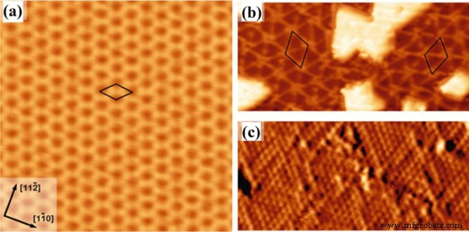
a のSTM画像 ハニカムTi 2 O 3 構造、および b Au(111)上に成長した風車TiO単分子層、および c Au(111)上の風車構造の原子分解されたSTM画像。 [83]
の許可を得て複製MoS 2 2DTMDCSファミリーの典型的な代表です。これまでのところ、バルク材料と単層でそれぞれ1.29eVと1.90eVの比較的小さなバンドギャップを持っているため、すべてのTMDCSの中で最も好ましいナノ材料の1つと見なされてきました[40、87、88]。以前は単結晶MoS 2 2Dフィルムは、ホストバルクから機械的に剥離されただけです。ダイレクトギャップ半導体であるため、MoS 2 の単層 理論上の限界である60mV dec -1 よりも鋭いターンオンを特徴とするバンド間トンネル電界効果トランジスタ(FET)の実現に興味深い可能性を提供します。 従来のトランジスタの場合、その結果、消費電力が小さくなります。間接ギャップ半導体であるシリコンの場合、バンド間遷移にはフォノンと再結合中心が必要であるため、この機能を実現することは依然として困難です[87]。 2D MoS 2 の興味深い最近のアプリケーションの1つ ナノクリスタルは、MoS 2 の単層に基づくトランジスタ[87]とフォトトランジスタ[40]です。 ナノシート。さらに、2Dフィルムの大面積蒸着の成功は、有機金属化学蒸着(MOCVD)、低圧化学蒸着(LPCVD)、誘導結合プラズマ化学蒸着(ICP-CVD)などの修正CVD技術によって達成されました。 )、または他の技術によって開発および組み合わされた他の革新的な方法。 CVDは、2DTMDC膜のウェーハスケール蒸着の機能でもよく知られています。図4は、興味深い例の1つが、超薄型2D MoS 2 のラガー領域堆積であることを示しています。 およびWS 2 4インチウェーハ上のフィルム[88]。このCVDプロセスでは、Mo(CO) 6 およびW(CO) 6 および(C 2 H 5 ) 2 SはMOCVD技術の前駆体として使用されましたが、H 2 / Arは、MOCVDプロセスでキャリアガスとして使用されました(図4a、b)[88]。 2D MoS 2 に基づく8100個の高性能FETユニットが実証されました フィルムは、同じバックゲート基板を使用したフォトリソグラフィー技術を使用して製造されました(図4c)。ユニットの2番目の構成では、外部SiO 2 誘電体膜が2DMoS 2 に堆積されました FET機器を製造するためのフィルム(図4d)。トランジスタの電気的測定により、さまざまなウェーハ部品から選択されたFETの一貫した性能が確認されました。したがって、2D MoS 2 のCVDプロセス中の均一でコンフォーマルな成長条件 およびWS 2 フィルムが確認されました(図4f)。
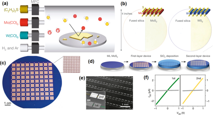
継続的なMoS 2 のウェーハスケールMOCVD成長 およびWS 2 映画。 a 2D MoS 2 のMOCVD用のCVDデバイスと関連する前駆体の概略図 およびWS 2 映画。 c 2D MoS 2 に基づく8100FETデバイスのバッチ Si / SiO 2 上のフィルム ウェーハ。挿入図は、100個のデバイスを含む1mm四方の拡大画像を示しています。 d 積み重ねられたMoS 2 の連続製造段階 ベースのデバイス。 e この画像は、MoS 2 を示しています 第1層と第2層のFETデバイス。 f 2つの異なる層にある2つの隣接するFETデバイスのIDS-VDS。 [88]
の許可を得て転載また、CVDは、さまざまな2Dヘテロ構造を製造するための用途の広い技術としての地位を確立しています[89]。たとえば、CVDは、横方向と縦方向の両方の構成の堆積を成功させるために採用されました。横方向のスタイルでは、2Dナノフィルムは原子レベルで一緒に結合されますが、縦方向の構造では、層間の相互作用力はvdWの性質を持っています。したがって、横方向の2Dヘテロ構造では、MoS 2 で報告されているように、2Dヘテロ界面の開発には厳密な格子整合が非常に必要です。 / WS 2 ヘテロ構造[89]。 MoS 2 のワンステップの簡単な堆積 / WS 2 硫黄、三酸化モリブデン、およびタングステンの前駆体がCVDプロセス中に使用されると、横方向の2Dヘテロ構造が確立されました(図5a、b)[89]。開発された2Dフィルムは、原子平面がアームチェアおよびジグザグ配向と同じ結晶配向を共有する鋭い原子ヘテロ界面を持っていました(図5c)。フィルムの最終的な形態は、MoS 2 を備えた三角形のコアシェル形状でした。 内部およびWS 2 外(図5d)。ラマン特性評価の研究により、垂直および横方向の2Dフィルムの両方の製造が確認されました(図5f)。開発 p-n 2D WS 2 間のヘテロ接合 およびMoS 2 フィルムは、2Dヘテロ構造フィルムの光起電力効果を強化しています。したがって、強いフォトルミネッセンス現象が検出されました(図5e、g)[89]。 WS 2 と同様の同じ結晶配向と格子構造を持つかなり鋭い界面 およびMoS 2 2Dフィルムが特徴づけられました。さらに、別のレポートでは、CVDを使用して横方向の1H MoS 2 を開発しました。 / 1T'MoTe 2 2つの成分が比較的大きな格子不整合を持っていたヘテロ界面[90]。 2D WSe 2 を含む、大きな格子不整合を持つ2DTMDCフィルム間のヘテロ界面の発達を示した他のいくつかのケースがあります。 / MoSe 2 [91]およびMoS 2 / WS 2 [92]半導体/半導体横方向2Dヘテロ構造の堆積のためのCVD法の能力を確認する。したがって、最新のCVD技術は、有機および高分子の柔軟な基板、絶縁体、およびグラフェン基板上に2D材料をうまく堆積させるためのその多様な機能を証明したと結論付けることができます。表1は、2D TMDCの最新の成果と、CVD技術によってウェーハスケールで製造されたそれらのヘテロ構造をまとめたものです[93]。
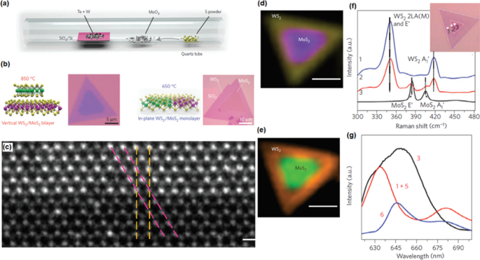
a 半導体/半導体ラテラル2Dヘテロ構造のCVD成長の概略図。 b WS 2 間の面内界面の原子分解能コントラストSTEM画像 およびMoS 2 。 c 351 cm -1 での2Dヘテロ構造2Dフィルムのラマン強度マッピング (黄色)および381 cm -1 (紫の)。 d 630 nm(オレンジ)と680 nm(緑)でのPL強度マッピングの組み合わせ。 [89]
の許可を得て転載および複製一般に、CVDで製造された2Dナノ材料とヘテロ構造の安定性は非常に高いですが、そのようなナノ構造の長期安定性に関する情報は、公開されているほとんどの作品でかなり限られています。 CVD成長TMDCベースの電子およびオプトエレクトロニクス機器の長期的な性能と安定性は、それらがキャリア散乱中心として機能することを考えると、ナノ材料の界面、欠陥、および粒界に大きく影響されます。これにより、デバイスのキャリア移動度が低下します。したがって、きれいな表面、高品質、ウェーハスケールのドメインサイズを備えた2D化合物材料の準備は、将来のナノおよびオプトエレクトロニクスにとって望ましい目標となるはずです。また、他の多くの2D複合材料はまだ十分に研究されていないか、うまく成長していないため、よりエキサイティングな発見が見つかるのを待っていることも強調しておく必要があります。
2Dナノ構造のALD
CVDの修正としてのALDは、厚さ制御された2D半導体およびサンドイッチ型ヘテロ構造の製造に向けたさまざまな戦略を実装できます。 ALDは最初は約45年前に開発されましたが、21世紀の初めになってようやく、大きな利点とさまざまな前駆体の開発により人気が高まりました[94]。過去10年間、酸化物、硫化物、セレン化物、テルル化物、窒化物、金属など、さまざまな種類の材料の製造に使用されてきました[95]。 ALDと他の蒸着法の主な違いは、すべての前駆体曝露後に自己飽和表面単分子層が形成されるという事実であるため、重要な要件は、適切な分子前駆体が自己制限反応を受けなければならないことです。 ALD化学の最新の開発の完全な説明は、最近のレビュー[94,95,96]にあります。 Thus, so far ALD has been implemented in a diverse number of fields including microelectronics [97], catalysis [98], photovoltaics [99] and sensors [100]. Unfortunately, the ALD implementation toward the synthesis of 2D semiconductors and 2D sandwich nanostructures is rather limited.
As deposition technique, ALD consists of a series of self-limiting, surface-saturated reactions to form thin conformal films at a controllable rate. Despite all obvious ALD advantages, it has to be admitted that this emerging technology has not yet been fully exploited for fabrication of different 2D nanostructures. Apparently, the lack of reliable recipes and precursors, specific ALD temperature window for deposition are some of the valid reasons for that. On the other hand, it was recently reported that the ALD advantages are far superior to the existing capabilities of other deposition techniques [101]. Specifically, ALD is the only one technology, which enables fabrication of defects-free, conformal 2D nanofilms and their heterostructures on the wafer scale with precise, Ångstrom scale control of their thickness during deposition [102]. In this regard, the state-of-the-art nanoscale ALD interfacing and molecular engineering of 2D nanomaterials can open up completely new possibilities by providing ultra-thin channels for key doping, minimization of the density of interfacial impurities and optimization of capabilities of instruments. Furthermore, the ALD fabrication technique enables turning the design of 2D nanostructures toward heterojunctions and hetero-structures [103,104,105], and hybrid SE based on inorganic–inorganic [106], organic–organic and inorganic–organic nanomaterials [107]. Figure 6 illustrates growing interests to ALD as well as comparison of the deposition rates and properties for 2D nanostructures developed by various deposition techniques [94].

Number of annual citations on “Atomic layer deposition” topic a of published manuscripts. Data are according to Web of Knowledge™ Database. Comparison of the deposition rate vs step coverage (b ) and coverage areas produced by different deposition techniques (c )。 Comparative analysis of properties of SE fabricated by PVD, CVD, and ALD, respectively (d )。 Reproduced with permission from [94]
ALD of 2D Metal Chalcogenide Films
The layered TMDCs are composed of sandwiched structure where the metal layers covalently bonded with two individual surrounding chalcogen atoms, thus the layer-by-layer deposition mechanism in ALD technique is favourable for making layered 2D TMDC nanostructures. Among the different 2D TMDCs films including binary, ternary and doped chalcogenides, less than 20 type of them could be deposited via ALD method. The first MoS2 nanofilm was fabricated by ALD in 2015. Initially, the number of MoS2 layers was controlled by the tuning of parameters of ALD technique [106, 108,109,110]. Later, the ALD synthesis of TMDCs monolayer was reported [111,112,113,114]. The self-limiting layer synthesis (SLS) of MoS2 monolayer film was also facilitated based on the typical ALD half-reactions [115, 116]. Here, the some practical cases of ALD of stable 2D films of metal dichalcogenides are summarized in Table 2 [94].
<図>The first investigation of 2D MoS2 deposition was based on the sulfurization of ALD deposited MoOx few-layered film. The formation of S–Mo-S arrangements of atoms along the z -axis was achieved after 10 min interaction of MoOx film with S gas at 600 °C [117]. The morphology, uniformity, crystallinity, nucleation and the quality of ALD-deposited film have direct impact on the final properties and characteristics of the MoS2 film [117,118,119,120,121]. In this example, the parameters of multistep annealing process should be controlled precisely to facilitate the formation of MoS2 films with sequential reduction of Mo and then incorporation of S atoms. In addition, the multistep reactions allowed the coverage control and phase transformation from crystalline MoS2 to the 2H-phase at the higher post-treatment temperatures. The first wafer-scale CVD of MoS2 on the 2-inch sapphire substrate was reported in 2014, when MoCl5 およびH 2 S were employed as the precursors in the ALD system at 300 °C [121]. It was found that 10 sequential ALD cycles are required to establish the uniform growth of the MoS2 film and prevent the islands growth. The following post-annealing of ALD MoS2 film at 800 °C improved the crystallinity of MoS2 at the expense of losing the thickness uniformity of MoS2 on the wafer substrates. Thus, higher number of ALD cycles were done (20 cycles) to compensate the lack of uniformity due to the high-temperature post-annealing process. Considering the ALD window, it was found that the ALD process within 350 to 450 °C permits higher quality of sulfide layers with the growth rate of 0.87 Å/cycles [122]. It was also demonstrated that the following annealing of as-deposited MoS2 film in H2 S or sulfur gas can improve the stoichiometry of 2D MoSx film [123].
The deposition of 2D MoS2 films via ALD technique can also be achieved by usage of other precursors. Other main precursors for deposition of MoS2 2D films were Mo(CO)6 , H2 S and dimethyl disulfide compounds. The ALD window suitable for these precursors is in the range of 155–170 °C. By monitoring the mass gain during the ALD cycles, it was revealed that multiple pulses of Mo source are required to reach the saturation, while a single H2 S injection is sufficient to saturate the reaction and achieve the growth rate of 2.5 Å/cycle in the optimized condition [124]. The plasma-enhanced atomic layer deposition (PE-ALD) can also be successfully employed to deposit ultra-thin h -MoS2 film on the different substrates. The growth rate of 0.5 Å/cycle was observed at the ALD window of (175–200 °C) for deposition of 2D MoS2 映画。 Lower ALD window (60–120 °C) caused the deposition of amorphous 2D MoS2 映画。 Particularly, the ALD at 100 °C allowed the formation of continuous layer of amorphous MoS2 on the Si wafer. To improve the crystallinity of as-deposited ALD film, the later rapid thermal annealing (RTA) treatment at 900 °C led to the formation of crystalline hexagonal layer of MoS2 [125, 126]. Another recipe for deposition of 2D MoS2 film is Tetrakis (dimethylamido) molybdenum (Mo(NMe2 ) 4 ), which interacts with either H2 S or alternatively 1, 2 ethanedithiol (HS(CH2 ) 2 SH) to deposit 2D MoS2 映画。 In this recipe, the ALD of MoS2 film taken place at the lower temperature (T < 120 °C) since the Mo(NMe2 ) 4 decomposes at temperature higher than 120 °C. The as-deposited 2D film was amorphous in this technique. Thus, the subsequent annealing was employed to crystalize the 2D MoS2 映画。 The mass spectroscopy analysis revealed that the mechanism of ALD deposition of MoS2 film is based on the removal of the remaining NMe2 ligands from the substrate surface after interaction of sulfur gas with Mo precursor. It was roved that it is possible to deposited 2D films on polymeric substrates by using lower ALD temperature.
2D WS2 is another example of the layered dichalcogenide ALD deposited at 300 °C by using WF6 およびH 2 S as precursors [127]. A Zn-based catalyst is required to initiate the deposition of WS2 film via ALD technique. Diethylzinc (DEZ) and H2 S were employed to assist the rapid nucleation of WS2 film over a wide range of substrates [128]. Zn acts as reducing agent for WF6 favouring the adsorption of WF6 on the surface of substrates. The initial growth rate of 1.0 Å/cycle was recorded, which then was reduced after 50 ALD cycles of WS2 沈着。 It was found that the deposition of a monolayer ZnS film is also facilitated the growth of WS2 film with crystalline structure [129, 130]
WSe2 is another TMDC 2D film which was fabricated by ALD [124]. In this report, a self-limiting approach for WCl6 and diethyl selenide (DESe) at the higher ALD temperature of 600–800 °C was employed and the dependence of film thickness on the ALD processing temperature was observed [131]. Five, three and one crystalized layers of WSe2 were deposited on the Si/SiO2 wafers (8 cm 2 ) at 600 °C, 700 °C and 800 °C, respectively. After 100 ALD cycles, the growth of WSe2 was stopped due to growth saturation. The deposited WSe2 film with few layers and monolayer was crystallined with honeycomb structure. The same film was employed as a p -type semiconductor in the FET and showed the capability of ALD deposited WSe2 film for application in electronic devices. In another parallel attempt, the thermal ALD of continues WSe2 film on the Si/SiO2 substrate was successfully carried out at 390 °C [132]. WCl5 およびH 2 Se were employed to deposit a highly uniform film with well-crystalline structure. The quality and crystallinity of the ALD WSe2 film were fairly compatible to the mechanically exfoliated and CVD WSe2 films [132].
SnSx 2D family is the other types of 2D materials which was extensively studied during last few years. The first deposited SnS film was reported by using tin (II) 2,4-pentanedionate (Sn(acac)2 ) precursor as the Sn source and H2 S as the sulfur source, respectively, where the growth rate of 0.23 Å/cycle was achieved in the ALD window from 125 to 225 °C. The other precursors for ALD of SnS film are bis(N 、 N ’-diisopropylacetamidinato) tin (II) (Sn(amd)2 ) and N2 ,N3 -di-tert-butylbutane-2,3-diamine tin (II) which react with H2 S gas during ALD [133]. This recipe enabled the deposition of crystalline SnS film at the ALD temperature of less than 200 °C.
2D SnS2 and SnSx films are deposited via employment of precursors containing Sn atoms [134]. The tetrakis (dimethylamino) tin (TDMASn) [135, 136] and tin acetate (Sn(OAc)4 ) [137] as the Sn (IV) metal precursors were used for ALD of SnS2 映画。 Polycrystalline hexagonal SnS2 films were deposited with the growth rate of 0.64–0.8 Å/cycle [134] at the temperature range of 140–150 °C. The growth of ALD temperature above 160 °C resulted in the development of thin mono-sulfide films. However, the as-deposited film always contains a combination of both mixed SnS and SnS2 compounds. Crystallinity of the film can still be improved by the following post-treatment annealing in H2 S gas at 300 °C. As an example, the formation of a single phased orthorhombic 2D SnS2 films with interlayer spacing of 0.6 nm was reported after the post-annealing treatment at 300 °C in H2 雰囲気。 Another precursor for ALD deposition of SnS2 film is Sn(OAc)4 where the ALD reaction in the ALD temperature of 150 °C resulted in the growth rate of 0.17 Å/cycle for the amorphous stoichiometric SnS2 映画。 Generally, in ALD deposition of few-layered SnSx films with Sn precursors and H2 S gas, the chemical composition, structure and the stoichiometry of SnSx ALD structures can be modulated depending on the deposition conditions and the post-ALD treatments [137].
One of the main ALD capabilities is the wafer-scale deposition of 2D hetero-structured TMDCs, which opens up further opportunity for fabrication of vdW hetero-structures. The technological challenges for deposition of 2D hetero-structured films are the main concerns for their deposition. Basal plans of the most of 2D materials are inert with the lack of dangling band, thus the nucleation of 2nd family of 2D films over the first layer is considerably challenging. Therefore, it is necessary to enable the initial adsorption of precursors on the surface of 2D film and then facilitate the growth of second 2D film over substrate. One of such examples is the ALD deposition of Sb2 Te 3 film on the surface of graphene by using SbCl3 and (Me3 Si)2 Te as precursors [138]. In this ALD process, (Me3 Si)2 Te was initially physically adsorbed on the graphene. The successful low deposition temperature of 70 °C for ~24.0-nm-thick crystalline Sb2 Te 3 layer was finally achieved with the crystalline plane parallel to the graphene substrates. A sharp hetero-interface was formed between the graphene and Sb2 Te 3 film as depicted on the high resolution transmission electron microscope (HRTEM) image in Fig. 7a [138].

a Cross-sectional image from the interface between ALD grown Sb2 Te 3 on graphene/SiO2 基板。 b The cross-sectional image of heterostructured Sb2 Te 3 / Bi 2 Te 3 stacked layers. c The HRTEM image of SnS/WS2 heterointerfaces and d the corresponding fast Fourier transform (FFT) image. Reproduced with permission from [138]
In another attempt, 2D hetero-structured Sb2 Te 3 / Bi 2 Te 3 metal chalcogenides films were deposited by the ALD process on Si/SiO2 wafer. Here, the bismuth telluride was selected to be deposited over the silicon wafer by the ALD technique at 165–170 °C, since it covers the Si better than Sb2 Te 3 。 Considering the low ALD temperature of Bi2 Te 3 (at 65–70 °C), the employment of initial long SbCl3 pulse in the ALD chamber was taken as a capable strategy to saturate the surface of Bi2 Te 3 and complete the surface reactions for the next deposition step [139]. This approach also facilitated the disposition of three stacking layers of Bi2 Te 3 /Sb2 Te 3 with a high level of crystallinity. Another example is the growth of multiple WS2 /SnS layered semiconductor hetero-junctions on the Si/SiO2 substrates by alternating ALD of WS2 and SnS at the ALD temperature of 390 °C [140]. The stacked 2D WS2 /SnS has the 15° orientation angle between their c axis originated from the difference in crystalline structures and the lattice mismatch between WS2 and SnS (Fig. 7b, c) [133]. This misaligned crystalline characteristics of WS2 /SnS hetero-interfaces is the origin of noticeable decreased of the holes mobility in SnS film [140]. Generally, the ALD techniques are recently undergoing consistent progress to enable the deposition of higher numbers of 2D TMDC films. However, there are still countless research opportunities to develop suitable ALD recipes for deposition of 2D TMDC films over the different substrates and also to develop nanoelectronic instruments based on 2D TMDCs.
ALD of Ultrathin Oxide Films
The few-nanometer-thick metal oxide films can be considered as 2D nanostructures when they can be assigned to few layers of 2D films. In this context, the characterization and exploration of 2D oxides properties for the practical applications are considered as valuable technical knowledge along with the progressive advancement in the device miniaturization. Furthermore, modern technologies use the advantages of ultra-thin metal oxide nanostructures as the main components of state-of-the-art nanodevices. Consequently, promising applications for the ultra-thin 2D semiconductors and insulators are expected, such as solid oxide fuel cells, catalyst films, corrosion protection layers, chemical sensors, spintronic devices, and UV and visible light sensors. Metal oxide semiconductor field-effect transistors (MOSFET) and the other novel nanoelectronic instruments are fundamentally dependent on the ultra-thin uniform films of metal oxides. Complementary, metal oxide semiconductor (CMOS) sensors are technically developed based on the deposition of ultra-thin metal oxide films which opened up a quite number of the different applications from image and light sensors to FET transistors in low-energy semiconductor instruments. The solar energy cells, plasmonic devices, data storage applications, bio-compatibility and bio-sensing features, supercapacitance properties, and electrochemical sensing are among the recently announced and discovered applications of the 2D oxide semiconductors. Thus ALD deposition of 2D metal oxide semiconductor thin films is considered as advanced fabrication technology. It is also an extremely difficult target to achieve considering the fact that the structural stability and molecular integrity of 2D films can be deteriorated easily. Accordingly, one of the main challenges is the versatile and conformal deposition of these 2D oxide nanostructures on the convenient substrates [94]. The following section is specifically focused on the ALD of metal oxide materials, and particular attention is given to molybdenum, titanium, aluminum, and tungsten oxide 2D films.
MoO3
Distinguishable properties of nanostructured molybdenum trioxide (MoO3 ) made it an excellent candidate for catalytic, electrical and optical applications. There are also several promising functionalities originated from the heterointerface between the MoO3 semiconductor and their metallic substrates. The bis(tert-butylimido) bis(dimethylamido) molybdenum ((tBuN)2 (NMe2 ) 2 Mo) is one of the precursors for MoO3 deposition, since it provides good volatility and thermal stability [141]. The PEALD window for molybdenum oxide with O2 plasma and ((tBuN)2 (NMe2 ) 2 Mo) precursor is in the range of 50–350 °C. The as-deposited films fabricated at the temperatures below 250 °C are usually amorphous, thus the post-deposition annealing process is needed to experience a transition from the amorphous to crystalline state. While the as-deposited films are sub-stoichiometric, the stoichiometry can be adjusted by the modulation of plasma parameters. The other precursors for ALD of ultra-thin MoO3 film is Mo(CO)6 which is mostly employed via O2 plasma to facilitate the low-temperature PE-ALD of MoO3 films in the narrow ALD window of 152–172 °C [141]. The resulted MoO3 film was deposited with growth rate of 0.75 Å/cycle. The as-deposited film was found amorphous with the oxygen deficiency at the heterointerface between substrate and MoO3 映画。 To achieve the crystalline structure, the following post-annealing at temperature above 500–600 °C is required. In another strategy, the ozone plasma was used on the surface of ALD MoO3 film deposited on 300 mm Si/SiO2 wafer [141]. Mo film was fabricated by using Si2 H 6 and MoF6 precursors at 200 °C. The wafer-scale deposition of ultra-thin MoO3 film over 4-inch Au on the Si/SiO2 wafer was reported, where C12 H30 N 4 Mo as molybdenum precursor and O2 plasma as oxygen source were used at two ALD temperatures of 150 and 250 °C, respectively. The process includes the pre-exposure of bare Au surface by O2 plasma which assists the formation of OH bonding on the Au surface. The following chemisorption of C12 H30 N 4 Mo molecules by the active sites on the Au and interaction with OH group on the surface of Au film led to the ligand exchange. The following O2 plasma completed the oxidation process and finalized the growth of ultra-thin monolayer MoO3 film (Fig. 8). The development of Mo–O-Mo bonding is expected after completion of oxidation process. Finally, 4.6-nm-thick MoO3 film was deposited over the wafer substrate. In this technique, the growth rate from 0.78 Å/cycle to 1.21 Å/cycle was measured when the ALD temperature increased from 150 to 250 °C [141].

a Graphical scheme of deposition of 2D MoO3 nanofilms by PE-ALD. b The injection of precursor into ALD chamber and c the reaction between precursor and Au surface (d ) and the complete deposition of a monolayer film over Au substrate. e The thickness of PE-ALD MoO3 film over Au substrate vs. the ALD cycle number at based on the usage of (NtBu)2 (NMe2 ) 2 Mo precursor and O2 plasma at 150 °C and 250 °C, with the precursor dosing time of 2 s and plasma exposure time of 5 s. f The saturation curve of (NtBu)2 (NMe2 ) 2 Mo precursor. The GPC is demonstrated as the function of precursor dosing time. g The saturation curve for O2 plasma showing the GPC as the function of plasma exposure time. Reproduced with permission from [141]
WO3

Enhancement of non-stoichiometry in monolayer WO3 film developed by ALD via intercalation/de-intercalation process
TiO2
Wafer-scale deposition of ultra-thin titanium dioxide (TiO2 ) film on the Si/SiO2 substrate was achieved by using the using tetrakis (dimethylamino) titanium (TDMAT) precursor and H2 O as an oxidation agent [145]. The optimum ALD temperature of 250 °C was selected for ALD of monolayer TiO2 film on the wafer-scaled substrate. To achieve a complete coverage of monolayer TiO2 , two individual ALD super-cycles were designed and implemented [145]. The first super-cycle consisted of 10 consecutive cycles of pulse/purge TDMAT to assure the reliable coverage of surface by precursors. Afterward, 10 pulse/purge stages of H2 O were performed to assure the completion of oxidation [145]. The XPS studies confirmed the changes of binding energies in both Si 2p and Ti 2p peaks after the deposition of 2D TiO2 could be elucidated by the development of Si–O–Ti bonds at the interface between native SiO2 and deposited 2D TiO2 映画。 The deposition of TiO2 on SiO2 substrate was accompanied by the decrease in binding energy of Si 4+ which was related to this fact that the silicon was more electronegative than titanium. The evidence of oxygen bridge bonding was also demonstrated by characterization of vibrational mode of Ti–O–Ti bonds in the FTIR spectrum of monolayer TiO2 and also by investigation of XPS spectrum of monolayer film [145]. The bandgap of 3.37 eV was measured for this TiO2 film with atomic-scale thickness. The capability of ALD for deposition of ultra-thin films is of great importance to functional applications like microelectronics and catalysis where only few ALD cycles are desirable. Table 3 summarizes practical cases for ALD development of various 2D metal oxides reported to date.
<図>In regard to stability of the ALD fabricated 2D nanostructures and their heterointerfaces, its mainly depends on the surface chemistry of ALD of 2D materials, especially because the inertness of their basal plans is expected to inhibit their growth and thus formation of vdW heterostructures. Moreover, as each precursor has specific “ALD window ” of deposition temperatures, trials and errors approach is required for optimization of the ALD fabrication temperature for each specific precursor taking into account the final thickness and porosity of deposited materials [98, 109]. Owing to the low deposition temperature, ALD of 2D oxides usually leads to fabrication of amorphous layers [32, 94]. Hence, when the crystalline phases of metal oxides are needed, post-annealing treatment is generally applied, improving the crystalline quality of the films as well as the interfaces with the substrate, which ultimately leads to the better stability of 2D nanomaterials over the time. Finally, although ALD appears to be a method of choice to fabricate oxide monolayers due to its precise control of the film thickness, only a handful of reports can be found in the literature [21, 32, 98, 141, 144, 145]. Therefore, the area of 2D metal oxide and their hetero-interfaces fabricated by ALD remains rather unexplored.
Self-limiting 2D Surface Oxides of Liquid Metals
The library of novel 2D materials for advanced applications is currently limited by the conventional synthesis methods of 2D films. The mechanical exfoliation of 2D films from their host layered bulks is not technologically precise and attractive method since the sizes distribution and thickness of produced nanosheets are not adequately and accurately controlled [146]. While the high vacuum techniques are accuracy of the depositing films are considered as high-quality films, these methods are still expensive, time consuming, and restricted by availability of precursors [64]. On the other hand, it is always desirable to introduce new synthesis methods of 2D materials in order to obtain the advanced 2D nanostructures with superior properties. Thus, synthesis of novel 2D semiconductor materials with distinguished or improved characteristics still remains a fundamental challenge.
Room-temperature liquid metals are a group of metals and alloys with unique electron-rich metallic cores which let them to stay in the liquid states even at the room temperatures. The interface of liquid metals with surrounding environment is the origin of one of the most natural 2D films [147]. This self-limiting surface oxide films (skin) is one of the most perfect planar materials with atomic scale thickness [148]. These crystalline structures are the host of unique properties and have provided a novel platform for synthesis of high-quality thin-film 2D materials for advanced applications [149]. Here, the liquid metals have the role of host material for synthesis of 2D films. With respect to the atomic structure, elemental composition, fluidity and thermodynamic of liquid metals, and furthermore, by considering the nucleation and growth characteristics of the surface oxide films, countless parameters are engaged to determine the proprieties of extracted 2D surface oxide films [150]. The low melting monophasic metal alloys are composed of post transition metals (Ga, In, Sn, Pb, Al, and Bi) and the elements of group 12 (Zn, Cd, and Hg). These elements can be combined together to produce a group of liquid alloys with low melting temperature. A biphasic liquid metal (mixture of solid and liquid) can be formed by either deviation of alloy composition from eutectic point or via adding solute elements above the solubility limit into the liquid metal solvent [151]. Gallium (Ga) is one of the most famous liquid metals with room-temperature melting point and possessing both covalent and metallic bonds at the solid state. The strong structural anisotropy and weak atomic bonding between Ga dimmers is originated from the distance between Ga neighbour atoms 2.7–2.9 Å which is considered as a significant distance between the gallium dimers [152]. This weak atomic bonding results in the weak crystalline structure in gallium which can easily break up at the room temperatures [153]. The alloying of Ga with some of the other elements may lead to further decrease in melting temperature of liquid alloy. One of the famous examples is the Ga-In alloy, when the melting temperature decrease to 16 °C in eutectic point of In-Ga alloy with atomic concentration of 14.2% indium [153]. The interface between gallium alloy and surrounding atmosphere is composed of the atomic-scale-thick gallium oxide (Ga2 O 3 )。 The liquid metal reacts with atmospheric oxygen even at very low oxygen pressure forming a self-limiting metal oxidation reaction [153]. This ultra-planar oxide films are among the most perfect naturally grown 2D materials [61]. This natural film prevents the liquid metal from the further oxidation. The ionic transfer through the natural surface oxide film is the controlling factor for the natural growth of surface oxide films of liquid metal and alloys. The formation of this oxide film leads to the highest reduction in the Gibbs free energy (ΔG f ) [154]. In a liquid metal alloy, the surface oxide film is mostly composed of surface oxide films of one of elemental oxide films of alloy components. The most famous example is the surface of oxide film of galinstan alloy. Galinstan (EGa, In, Sn) is the eutectic alloy of gallium–indium–tin. However, the surface oxide of galinstan is composed of Ga2 O 3 。 Since the ΔG f of Ga2 O 3 is lower than that of In2 O 3 およびSnO 2 in oxygen atmosphere, the surface oxide of galinstan alloy is mostly composed of Ga2 O 3 [155]. With the same synthesis strategy, it is possible to synthesize the mixed 2D oxide films similar indium–tin–oxide. To this aim, the molten In–Sn alloy should be used to extract 2D films from the surface of liquid In–Sn alloy [154].
Due to the nonpolar properties of liquid metals, the attraction force between the liquid metal and its natural surface oxide film is weak and localized. Thus, a weak mechanical force can simply delaminate the surface oxide films from the surface of liquid metals. The delamination of surface oxide film can be achieved via the mechanical separation and exfoliation of 2D films by applying mechanical exfoliation methods including sonication, touching of liquid metal with the appropriated selected substrate, mechanical rolling of the liquid metal and alloy over the smooth substrate and separation and extraction of 2D films through the density differences and gradients between the synthesized compounds. These methods were employed recently for delamination of several different types of the surface oxide films of liquid metals from their host alloy. The following section will review some of lately synthesized 2D surface oxide films of liquid metals and alloys.
SnO x
2D SnOx film was successfully delaminated via vdW exfoliation of the liquid tin surface oxide film. Elemental tin (Sn) with its low melting point (231.9 °C) [156] and its high conductivity (9.17 × 10 6 σ) is used as electrical connections in the electronic utensils. The anti-corrosion impact of tin oxide layer has been confirmed before. SnO 2 naturally covers the surface of tin alloy under the atmospheric condition and prevents further oxidation of Sn [156]. It was found that the natural surface oxide film of liquid tin in the ambient atmosphere is composed of a mixture of tin oxides which is predominantly composed of SnO2 , with some contributions of SnO, Sn2 O 3 and Sn3 O 4 [156]. The precise control of oxygen exposure to the surface of fresh molten tin is the main technical factor to determine the composition of surface oxide film of tin alloy. This is a highly important factor during the synthesis of the surface oxide film of molten tin, when we take into consideration the fact that the SnO2 is n- type semiconductor, and SnO is a p -type semiconductor with a variety of different electrical properties. The bipolar characteristics of SnO is another important properties of this material which made it a functional choice for application in electrical invertors [157]. Furthermore, the high stability and sensitivity of well-established SnO films turned them to the desired option for application in chemical-based FET sensors and catalyst films. The transparency is another characteristic of SnO films originated from the wide bandgap of this semiconductor [156, 157].
To exfoliate2D SnOx film, the fresh surface oxide film of molten tin was mechanically delaminated by the contact of surface of Si/SiO2 substrate with the surface of molten alloy inside of the glove box [158]. The scheme of process was graphically demonstrated in Fig. 10a [158]. The delaminated SnOx film in ambient atmosphere had ~ 0.6 nm thickness [157] with crystalline structure. Considering the interlayer spacing of crystalline SnO (0.484 nm), 0.6-nm thick film can be considered as a monolayer SnO film and 1.1-nm-thick film is therefore a bilayer SnO 2D film (Fig. 10b). The 2D films synthesized in glovebox and under oxygen concentration of 10–100 ppm had ultra-fine surface characteristics. The measurement of interlayer spacing showed that the nanosheets formed under ambient atmosphere were composed of two distinct materials with interlayer spacing of 2.7 Å and the other 3.35 Å, which were respectively attributed to the crystal lattice of SnO and SnO2 。 The 2.7 Å lattice spacing was related to the (110) plane of SnO, while the 3.35 Å lattice spacing was attributed to the (110) plane of SnO2 , respectively (Fig. 10c–e) [158]. The sample synthesized in the reductive atmospheres was mostly covered by SnO film. The bandgap measurement of SnO film showed the direct bandgap of 4.25 eV. This ultra-thin 2D film was employed to fabricate the SnO-based FET transistor. p -type characteristics of SnO-based developed FET was confirmed with the mobility of 0.7 cm 2 V -1 s -1 (Fig. 10g) which was much higher than the similar FET devices based on the pulsed layer deposited bilayer SnO film with the mobility of 0.05 cm 2 V -1 s -1 [159].

a Graphical representation of vdW exfoliation method. When a Si/SiO2 substrate is attached to the molten tin alloy, the created vdW force between the tin oxide and SiO2 surface help to delamination and following attachment of 2D oxide film to the SiO2 基板。 b The AFM image of the monolayer (0.6 nm) and bilayer (1.2 nm) tin oxide film. c The TEM image of tin oxide film developed in controlled atmosphere. d The HRTEM of tin oxide film developed in ambient atmosphere with mixed SnO and SnO2 構造。 e The HRTEM image of SnO film developed in controlled atmosphere. f The bandgap of monolayer SnO film measured by electron energy loss spectroscopy. g The I-V characteristics of fabricated SnO FET device at various gate voltages. Reprinted with permission from [156]
GaPO 4
The high-temperature stable gallium phosphate (GaPO4 ) semiconductor (up to 930 °C) is one of the functional piezoelectric semiconductors with outstanding technical position compared its rival of α-quartz [61]. Gallium phosphate has trigonal structure with the cell parameters of a = 4.87 Å and c = 11.05 Å and γ = 120° (Fig. 11a) [160]. The piezoelectricity facilitates the mutual conversion of electrical energy or pulses to mechanical forces or oscillations. To develop miniature power and electric instruments and generators, it is highly required to synthesize 2D piezoelectric materials for novel nanoelectronic technology. In this device, the atomistic level vibration, bending and displacement can be monitored and then facilitate the harvesting of kinetic energies of oscillation of piezoelectric materials. The loss of centro-symmetry is the main structural specifications of 2D materials with piezoelectric properties [160]. Many types of 2D materials including, TMDCs with odd number of layers, transition metal oxides, aluminium nitride, GeS and SnSe2 、 h -BN and graphene are capable of showing the piezoelectric properties [161,162,163] at the low temperatures. Nowadays, it is highly required to synthesize new 2D materials with stable piezoelectric performance at high operational temperatures. This is very challenging issue since the performances of 2D piezoelectric materials are failed due to the structural changes at the high working temperatures. Another difficulty arises from the challenging deposition stage of homogeneous 2D piezoelectric films of functional instruments.

a The side view of GaPO4 demonstrating the out-of-plane structure of GaPO4 。 b For the secondary phosphatization treatment. c The AFM and HRTEM studies of 2D GaPO4 映画。 d The XRD, e Raman and f bandgap measurement of 2D GaPO4 映画。 Reprinted with permission from [160]
As a successful achievement, the 2D archetypal piezoelectric GaPO4 film was recently synthesized via processing of 2D surface oxide film of gallium. The archetypal piezoelectric GaPO4 is not naturally available in crystalline scarified structure [160], and thus the conventional mechanical exfoliation techniques are not capable of synthesis of 2D crystalline gallium phosphate films. In this method, natural surface oxide film of gallium was mechanically exfoliated from its liquid alloy via vdW delamination technique, see Fig. 11b. The secondary post-annealing treatment was employed inside a furnace for the secondary phosphatiation treatment [61]. The vapor gas containing phosphor chemically interacted with the surface of 2D Ga2 O 3 film by the heating of H3 PO 4 粉末。 N 2 gas had the role of carrier gas for transfer of vapor phosphor gas to the surface of 2D Ga2 O 3 film at 300–350 °C (Fig. 11b). The following AFM and HRTEM measurement of samples confirmed the synthesis of 1.1-nm-thick 2D film with dimensional characteristics similar to the trigonal GaPO4 in the c crystalline direction (Fig. 11c) [160]. The XRD studies and Raman characterization have confirmed that 2D GaPO4 film had crystalline structured with dominance of (003) and (102) planes of trigonal α-GaPO4 。 (Fig. 11d, e). A wide bandgap of 6.9 eV was measured for α-GaPO4 film (Fig. 11f). The experimental measurements reaffirmed the strong out-of-the-plane piezoelectric properties for the GaPO3 2D nanostructures which was around 8.5 pm V −1 [160]. This considerable piezoelectric characteristics of 2D α-GaPO4 highlighted the capability of this synthesis method to develop novel 2D materials with distinguishable mechano-electric properties.
GaN
The same post-processing approach was employed to synthesize GaN and InN 2D films from the surface oxide film of liquid gallium and indium [160]. The technique is based on squeeze printing of liquid gallium droplet between the Si/SiO2 parallel substrates (Fig. 12a). In contact with atmosphere, Ga liquid was instantaneously oxidized in atmospheric condition. The synthesis process resulted in the formation of 2D Ga2 O 3 films with thickness of 1.4 nm [157]. The following ammonolysis reaction at 800 °C was operated in the presence of urea. It was found that lower reaction temperatures did not facilitate the conversion of Ga2 O 3 into the wurtzite GaN films (Fig. 12b) [160]. The thickness of the film after ammonolysis process was found to be 1.3 nm which is corresponded to the to three wurtzite GaN unit cells (Fig. 12c). The lattice constant of 5.18 nm was measured for 2D GaN film. The TEM studies also confirmed the crystalline structure of GaN with interlayer spacing of 0.28 along the (001) crystalline plate (Fig. 12d) [160]. The X-ray photoelectron spectroscopy (XPS) affirmed the substantial amount of nitrogen was replaced by the oxygen atoms in GaN structure which is owing to the similar bond length of Ga-O and Ga-N. It was targeted to decrease the level of oxygen in 2D GaN films. However, the successful removal of oxygen from the 2D GaN films was not achieved even during the synthesis process at the high temperatures. A bandgap of E g = 3.5 eV was measured for 2D GaN film (Fig. 12e) compared with that of Ga2 O 3 映画。 The reason for the considerable decrease in the bandgap was attributed to the upward shift of the valence band of GaN film due to the hybridization of the O2p -N2p orbitals [160].

a Schematic illustration of squeezing of liquid metal galinstan between SiO2 substrate and b following post-ammonolysis treatment for phase transform of Ga2 O 3 to GaN film. c The High resolution AFM image of the surface of GaN film. d The HRTEM image of GaN film and e the band gap of measurement of GaN film. Reprinted with permission from [160]
The similar strategy was used to synthesis 2D InN film via two-step synthesis technique [160]. In this method, the vdW exfoliated 2D In2 O 3 film was extracted from the surface of liquid indium. An intermediate bromination step was performed to transfer In2 O 3 to InBr3 。 A 20-s post-processing stage of In2 O 3 film adjacent to HBr source was enough to complete the phase transformation from In2 O 3 into InBr3 [61]。 The following ammonolysis treatment of InBr3 2D film by NH3 source at the temperature of 630 °C resulted in the phase transformation of InBr3 into InN [160]. The following characterization studies confirmed the development of crystalline 2D ultra-thin wurtzite InN nanostructures with the crystalline lattice constant of 5.5 Å with the bandgap of 3.5 eV [160]. Generally, the multi-step synthesis technique was found as reliable approach towards the synthesis of advanced 2D nanostructures by using the surface oxide of liquid metals. The developed 2D nanostructures have clearly demonstrated novel electronic and optoelectronic characteristics which are not expected and observed in the similar 2D nanostructures, synthesized via high-vacuum deposition-based methods [164].
SnO/In 2 O 3 2D Heterostructures
The p-n heterojunctions are now the building blocks of the semiconductor devices where the hetero-interfaces between two semiconductor materials with the different types of charge mobility properties are used to fabricate various types of electronic and opto-electronic instruments. Specifically, the heterostructured devices based on 2D films can be developed by several different approaches and techniques including mechanical exfoliation from the host material, CVD, ALD, molecular beam epitaxy, and pulsed laser deposition [165, 166]. Interesting new strategy was recently employed to fabricate vdW heterostructured 2D layered materials via stacking of various 2D layered crystals extracted from their liquid-based metals and alloys. A p-n heterojunction was developed by the vdW exfoliation of 2D SnO and In2 O 3 films [167]. In this method, 2D SnO/In2 O 3 vdW heterostructures developed [167] by the vdW transfer of surface oxide film of liquid tin (p -SnO) on top of the natural surface oxide of indium (n -In2 O 3 )。 The developed 2D heterostructured film finally composed of p -SnO/n -In2 O 3 2D films attached on top of each other via vdW forces (Fig. 13a, b) [167]. The following microstructural studies in atomic scale levels confirmed the formation of a vdW heterointerfaces between SnO/In2 O 3 films with two crystalline structures with the different characteristics fabricated over Si/SiO2 substrate (Fig. 13c). The lattice spacing of 0.27 nm corresponded to the (321) plane of crystalline In2 O 3 , and the other 2D film with 0.298 Å is attributed to the (101) plane of SnO. The heterostructured film had the thickness of 4.5 nm (Fig. 13d, e). The Raman and optical characterization studies confirmed the development of heterointerfaces with optical absorption peak of SnO/In2 O 3 film located at 251 nm, which was a number between 246 nm (SnO absorption peak) and 256 nm (In2 O 3 absorption peak in Fig. 13f, g) [167]. One of the main properties of heterostructured film was strong interlayer coupling of charge carriers which affected the optical absorption of 2D film. The bandgap of heterostructured film was narrowed to 2.30 eV while the bandgap of individual SnO and In2 O 3 were 4.8 eV and 3.65 eV, respectively, [167]. The schematic of band alignment at 2D SnO2 /In2 O 3 vdW hetero-interfaces was demonstrated at Fig. 13h. The effective bandgap at p–n junction was expected to be 2.30 eV, which was close to the calculated value of band gap of 2D heterostructured film from Tauc plot. The narrow bandgap assisted the charge separation at hetero-interfaces, thus the photoexcited electron–holes can be separated easily and they can feasibly migrate from the valence band of SnO to the conduction band of In2 O 3 映画。 The specific energy band alignment at the hetero-interfaces of vdW SnO2 /In2 O 3 demonstrated quite impressive capabilities and excellent photodetectivity of 5 × 10 9 J with the photocurrent ratio of 24 and the outstanding photoresponsivity of 1047 A/W [167]. Here, the liquid metal printing technique was found as the valuable potential approach for fabrication of heterostructured 2D materials, which do not naturally exist as the layered structures in nature.

a Schematic illustration of fabrication of 2D vdW heterostructured SnO/In2 O 3 映画。 b The HRTEM image of heterostructured SnO/In2 O 3 映画。 c The HRTEM image of atomic structure of heterostructured films show the high crystalline structure of SnO and In2 O 3 film with their lattice spacing distance. d The AFM of heterostructured SnO/In2 O 3 film with e the profile thickness of the films. f The Raman spectra of SnO, In2 O 3 and SnO/ In2 O 3 2D films. g The optical absorption of SnO, In2 O 3 and SnO/ In2 O 3 2D films. h The band alignment of SnO/ In2 O 3 2D heterostructures. Reprinted with permission from [167]
Therefore, the natural ultra-thin metal oxide films on the surface of liquid metals and alloys were found as functional materials with tremendous applications. Ultra-thin nature, pin-hole free and considerable lateral dimensions of these films accompanied by the facile vdW delamination of them on desired substrate provided a great platform for successful synthesize of novel generation of 2D materials and related electronic instruments [168]. Table 4 has provided a representative information on the recently developed 2D materials and devices based on 2D surface oxide film of the liquid metal and alloys.
<図>Novel Applications of 2D Semiconductors
Memristors Based on 2D Semiconductors
The information technology today faces the fast growing of amount of generated data. The data processing in new era requires development of advanced data storage technologies far beyond of concept of current silicon-based technology. Today Si-based memories are facing their technological limits, furthermore, the complementary CMOS instruments are also suffering from the physical dimensional retractions and technological problems [169]. Consequently, it is highly required to develop new nanostructured materials with improved properties and also to modify the existing devices to circumvent the technological restrictions related to the storage capacity of memory units. The von Neumann technology tries to emulate the working mechanism of human brain where the complicated networks of interconnected biological synapse enable us to memorize, learn, remind, recognize, process and understand the multi-task operations with minimum energy consumption. An average power consumption for a singular synaptic event is in the range of 1–10 fj, which is at least 5 orders of magnitude lower than the energy consumption of the existing conventional computers [170]. The current von Neumann technology architecture is not efficient since their memory and processing units are physically separated. A low-energy consumption non-volatile memristors with nanoscale dimensions, high performance, and improved processing speed can respond the current memory technology which is in its bottle-neck stage [170]. Regarding the energy consumption issues, 2D materials can be employed as ultra-thin nanostructural memristors. The resistive switching (RS) behavior of 2D materials has also been explored recently. It was found that the employment of 2D materials in memory units could potentially tackle the current limitations in memory devices [171]. Recently, the nonvolatile characteristics of 2D materials have been extensively investigated and characterized. The 2D semiconductor layered materials and ultra-thin oxide films possess a wide range of properties in various fields which also can be accompanied by their memristive characteristics.
Memristors Based on TMDCs
The recent development in nanodevice fabrication technology enabled the employment of ultra-thin TMDC films in functional instruments. The CVD and metal organic CVD were successfully employed to deposit monolayer MoS2 、MoSe 2 、WS 2 , and WSe2 2D films in a sandwiched in a vertical configuration between Au electrodes over Si/SiO2 substrate (Fig. 14) [172]. It was confirmed that monolayer TMDC films had no grain boundaries and they are empty of oxide compounds. Thus, an oxide free hetero-interface was shaped between Au electrodes and 2D TMDC films. This sharp and clean hetero-interface increased the possibility of precise measurement of electrical properties of 2D films. The graphical scheme of the memristor devices, the top view of device and the cross-sectional TEM image of Au/MoS2 /Au memristor are presented in Fig. 14a–c, respectively. The characterization of 2D MoS2 by atomic resolution scanning tunnelling microscope (STM) (Fig. 14d) demonstrated relatively high quality and additionally showed local sulfur vacancy defects in the MoS2 映画。 The unit based on monolayer MoS2 film verified high on /off 10 4 を超える比率 and the corresponding retention time as high as 10 6 s。 The bipolar resistive switching was observed in the behavior of all memristors based on MOS2 、MoSe 2 、WS 2 , and WSe2 2D films. Both unipolar and bipolar resistive switching behavior were detected during the study of resistive switching response of MoS2 映画。 The abrupt increase of the device current in all samples indicated the occurrence of dielectric break down phenomenon. The formation of conductive filaments (CFs) in the 2D active layer of memristors was the main mechanism of RS (Fig. 14e–i). Thus, the electroforming can be avoided by scaling down the thickness of active memristor layer into the few nanometer range. The main drawback of this strategy is the excessive leakage current originated from the trap-assisted device tunnelling [165]. Occasionally, the unipolar RS was observed in the certain single-layer MoS2 metal/insulator/metal units as was shown in Fig. 14 f. The typical bipolar RS behavior was also presented in the study of resistive behavior of atomristors based on monolayer MoSe2 、WS 2 およびWSe 2 films, respectively [172].

a Schematic interpretation of metal/insulator/metal atomristor device based on TMDCs monolayers, b the corresponding optical image of device and the c cross-sectional TEM image of Au-Monolayer MoS2 -Au device. d The atomically resolved STM image of monolayer MoS2 film deposited on Au electrode. The sulfur vacancies indicated by dashed lines. e The typical I-V curve of atomristor device based on monolayer MoS2 monolayer device. The typical bipolar RS behavior is observed. f The occasional unipolar RE behavior of device in monolayer MoS2 端末。 g 、 h および i graphs respectively demonstrate the typical bipolar RS behavior of atomristor devices based on monolayer MoSe2 、WS 2 およびWSe 2 映画。 Reprinted with permission from [172]
In another configuration, a memristor based on monolayer MoS2 was developed where a Cu electrode was employed as the active electrode to fabricate electrochemical metallization memory device [173]. In this instrument, the Au film play the role of inert conductive electrode. The scheme of this device is demonstrated in Fig. 15a. Due to the diffusion of Cu ions in MoS2 layer a conductive atomic-scale Cu filament is formed in the MoS2 double monolayer. Therefore, this memristor falls under the category of electrochemical metallization memories (ECM), whereas the memristive performance of other 2D MoS2 device with the inert electrode (similar Au) is based on migration of the sulfur vacancies. The sulfur vacancies in MoS2 thin films make conductive filaments with atomic scale dimensions, and hence these types of MoS2 memristors are known as the valence change memories (VCM) [173].

The optical image of Cu/MoS2 double layer/Au memristor device with scale bar of 100 μm accompanied by the graphical scheme of device with top Cu electrode and bottom Au electrode. The memristor’s crossbar area is 2 × 2 μm 2 。 b The I-V curve of memristor device with bipolar RS with the 0.25 V Set voltage and − 0.15 V Reset voltage. e The logarithmic scale I – V curve of device for the pristine state before and after forming process, and for LRS and HRS after the forming process. Reprinted with permission from [173]
In fabricated ECM (Fig. 15), the two-dimensionality and electrochemical metallization by Cu cationic filaments resulted in the considerable decrease in switching voltage down to 0.2 V (Fig. 15b). This characteristic has arisen from the lower diffusion activation energy of Cu cations in MoS2 layer compared with that of sulfur vacancies in 2D MoS2 film [173]. The bipolar resistive switching was the main characteristics of the I-V curve of memristor with a set voltage at 0.25 V and a reset voltage at − 0.15 V. It was observed that the majority of double-layer MoS2 memristors are free of the forming process. By using a double-layer MoS2 memristor the transport mechanism in Cu/double layer MoS2 /Ag device was investigated. Figure 15b depicts the I–V characteristics of memristor before the forming process (pristine state) as well as for HRS and LRS (after forming). The instrument performed in pristine state with the resistance of 16.6 kΩ when the applied voltage on the unit was less than 0.3 V. Quantum tunnelling was recognized as the conduction mechanism in memristor in the pristine state. In this condition, the resistance is much larger than the resistance of device after the forming process of memristor. The further increase of applied voltage beyond the 0.3 V in pristine state is accompanied by the transition in I–V curve into the slope 2 region (I ∝ V 2 ), which corresponds to the space-limited conduction states. The dramatic increase of current after increasing of applied voltage (further than 0.6 V) is attributed to the formation of Cu conductive filaments in MoS2 film (Fig. 15c). Higher imposed voltage on Cu electrode resulted in the oxidation of Cu top electrode. This resulted in the migration of Cu cations toward the bottom Au electrode to reduce and deposit there. The conductive Cu filaments were built up along the defective grain boundaries of 2D MoS2 film and the device switched to LRS.
Complementary Resistive Switching in Transition Metal Oxide Films
The ion doping of semiconductor films can tangibly alter the charge transfer mechanism in these ultra-thin films. The memristive characteristics of 2 semiconductors are also tangibly affected by the presence of other foreign ionic species inside active materials of memristors. TiO 2 is one of the well-known recognized semiconductors with resistive switching characteristics. A 7.0-nm-thick TiO2 ALD film was used to investigate the impact of ion intercalation in resistive switching of this ultra-thin film [174]. To understand the effect of Indium (In) intercalation in active layer of memristor (TiO2 ), an ion incorporation set up was made. The ion intercalation in this set-up was facilitated by imposed driving voltage on the ion-containing solution covering the surface of 2D TiO2 映画。 The potentiodynamic measurements (I–V sweep) of Pt/TiO2 /Au and Pt/In-doped TiO2 /Au memristor under the dark condition showed different RS mechanisms for In-ion doped and non-doped TiO2 映画。 Pt/TiO2 /Au device shows bipolar switching behavior (Fig. 16a). V セット = 0.94 and V Reset = − 0.98 during I–V sweeping measurement were observed [174]. A bipolar RS behavior of film was explained by the ionic drift of oxygen vacancies owning to employed voltage on the electrochemically inert Au and Pt electrodes. This unit is categorized as VCM cells. The schematic representation of oxygen vacancies distribution for both off and on states are shown in Fig. 16b and c. The dielectric member of memristor is characterized with two parts:low conductive TiO2-x with the thickness of t and insulating part with the thickness of D-t 。 The applied voltage on the electrode caused the ionic drift of oxygen vacancies, which is accompanied by the shift of border between low conductivity component and insulating part of active layer of memristor. In this condition, the I–V curve of device is not further Ohmic and will be non-linear. In this proposed model, the thickness of insulating layer should be small enough (few nanometer) to let the electric field develops and promotes the ionic drift of defects [174].

a Typical logarithmic scale depiction of I–V sweeping graph of Pt/In-doped TiO2 /Au memristor. b Device is set off, the metallic cations are distributed in top layer of In-doped TiO2 映画。 c The formation of filamentary conductive channels, the device is set On (Set, stage 1). d The depletion of metallic cations adjacent to the bottom electrode. The device is set off again (Reset, stage 2). e By imposing the reverse gate voltage, the metallic cations again move toward the cathode electrode (top Pt electrode) and again form a metallic cation bridge and the device is set On (Set-stage 3). f By depletion of metallic cations, at Pt electrode the device is set off again (Reset, stage 4). Reprinted with permission form [174]
The In-doped TiO2 film demonstrated a complementary resistive switching (CRS) behavior during the voltage sweeping between − 1.0 V and + 1.0 V (Fig. 17a) device is set at a higher voltage and again reset at another lower voltage of the same polarity [174]. The cell was set for the first time at V Set1 = 0.732 V and then reset again in the same polarity at V Reset1 = 0.1277 V. In the negative voltage, the second LRS to HRS switching occurred at V Set2 = − 0.7055 V and again reset to HRS at V Reset2 = − 0.0901 V. Thermally assisted charge transfer mechanism is the most possible theory which explain the resistive switching in the ion-doped TiO2 2D film. The unipolar switching confirms the filamentary nature of resistive switching. The filamentary resistive switching is mostly based on the ECM of the mobile ionic species caused by the migration of metallic cations. It facilitates the development of filamentary metal bridges (on state), which can be ruptured later (off state). The filamentary mechanism is the characteristic of this memristor, which is fabricated with electrochemical active electrodes, while the In-doped TiO2 memristor was sandwiched between inert Au and Pt electrodes. It is expected that the switching behavior of In-doped TiO2 device was originated from the migration of both anion and cation components. The versatile switching behavior of In-doped TiO2 device can prove that both anion and cation components are involved in CRS mechanisms. The proposed model suggested that the redistribution of oxygen vacancies and Indium ions inside TiO2 layer can affect, alter and facilitate the RS. In the heterostructured oxide stacks, the conjunction of an oxygen deficient oxide layer (LRS mode) with another oxygen rich layer (HRS mode) triggers the CRS of heterostructured memristor which is caused by the movement of oxygen vacancies. This gradual change of oxygen concentration can trigger occurrence of CRS of memristor due to the difference in resistance of TiO2 スタック。 From another point of view the formation of filamentary conductive channels assist the RS and increase the conductance of devise. At the initial state or off state (Fig. 17b), the top In-doped layer is in LRS mode while the bottom layer is in HRS. By applying the threshold voltage, the ionic species migrate into lower insulating layer resulting in the formation of conducting filaments and paths (Fig. 17c) and then device reaches to its on state (Set 1). At higher positive voltage, the ionic species in upper layer (mostly In-ions) are depleted (Fig. 17d) and again device will reach to its off state (Reset 2) and demonstrates HRS behavior. The similar phenomenon is expected to occur at the negative biases in which the first on state (Fig. 17e) switches the memristor to new LRS, following another off state after depletion of the ionic species (Fig. 17f). The versatility of CRS behavior of all samples was repeatedly tested several times and the same behavior was observed.

The Pt/TiO2 /Ti/Pt stacked crossbar cells:a the SEM top view of (60 nm) 2 cross-point, b The TEM cross-sectional image of 100 nm 2 Pt/TiO2 /Ti/Pt device with c its corresponding schematic graph of the plug and disc region in the TiO2 層。 Reprinted with permission from [174]
Artificial Optical Synapses Based on 2D Semiconductors
The human brain operation is highly energy efficient. The data storage and processing are functioned in brain with the lowest possible energy consumption. This ultra-low energy consumption is inspired by the functionalities of biological nervous system. Based on the brain performance, a novel type of computing and processing system was proposed by Alan Turing in 1948, when he introduced the idea of using a computing device with the interconnected network of artificial neurons [175]. It is envisaged that the interconnect network of artificial synapses can effectively solve and overcome the restrictions of the traditional van Neumann computing. The biological synapses, as one of the key members of the neural system, are the information channels ensuring short-term computation, long-term learning and memorization by tuning the synaptic weights [176]. As a biological structure, a chemical synapse is a gapped connection between two neurons through which the communication between two individual axons is created by biochemical reactions. The synapse is a biological junction where the electrochemical waves (action potentials) are transmitted through the axons of neuron. The energy consumption of a biological synaptic event is tangibly lower than that of any other similar device. Analogously, an artificial synapse is a unit which mimics the behavior and performance of the biological synaptic junction to transfer the synaptic signals. From the technical point of view, memristors are the best candidates capable of successful emulation of the characteristics of a biological synapse [177]. The resistive switching mechanism is the basic principle of the memristors. A sandwiched insulator or transition metal oxides between two conductive electrodes is the typical structure of an artificial synaptic device. The synaptic properties are observed in variety of materials with different resistive and synaptic mechanisms. In fact, the diversity of materials with synaptic characteristics experiences a rapid progress, and thus the fundamental understanding of related synaptic mechanisms is currently progressing. Metal oxide resistive random access memories (RRAMs) (such as TiO2 , AlOx , HfOx , WOx , TaOx ), conductive bridge synapses (Ag- and Cu-based electrodes), phase-change material-based synapses (PC synapse), ferroelectric material-based synapses, magnetoresistive (MR)-based synapses, carbon nanotube based synapses, and organic nanostructured-based synapses are some of the active memristor materials that demonstrated attractive synaptic characteristics [177]. The optical stimulated synaptic devices are recently introduced into telecommunication technology. In optical synapses, optical pulses of light stimulate the generation of charge carriers between two conductive electrodes. The photogenerated charge carriers in atomically thin 2D MoS2 film allow the modulation of the synaptic weights with photonic pulses. This optical capability of artificial synapse is highly important that capitalizes the possibility of high-bandwidth optical communication protocols. The schematic of 2D MoS2 -based synaptic unit is depicted in Fig. 18a [178]. As the main privilege, the incorporation of the optical and electrical pulses addressed the different charge trapping mechanisms to precisely modulate the synaptic weights. Furthermore, the instrument was capable of neuromodulation to achieve the plasticity and metaplasticity properties via dynamic control of spike-time-dependent plasticity (Hebbian theory). The schematic of analogue circuit is demonstrated in Fig. 18b depicting the interplay between Hebbian and homeostatic plasticity. The interplay between Hebbian and homeostatic synaptic plasticity in MoS2 synapse is provided in Fig. 18c–e, respectively. The long-term potentiation strength was achieved by employment of sequential voltaic training pulses in synaptic instrument. It was observed that the synaptic weights increase linearly by increasing the number of training pulses. It was also demonstrated that the application of 100 training pulses resulted in the weight change of synapse up to 117% in electronic mode, while the same number of training pulses in ionotronic-mode resulted in the increase of weight up to 223%. (Fig. 18c, d) [178]. In the optically stimulated synaptic unit, a strong long-term potentiation was observed in the 2D MoS2 artificial synapse via using the optical gating function (Photoactive mode). The light pulses (λ = 445 nm) played the role of presynaptic signals. Up on the illumination on the surface of 2D MoS2 synapse, the conductance increased rapidly and then continued until the gradual saturation when the conductance was one order of magnitude above the value of dark-current. A rapid drop of conductance occurred on the termination of optical illumination source, but the conductance still remained in high values (Fig. 18e). The band-to-band transition is expected to be the main reason for rapid transition, while the long-lasting high conductance values in optoelectronic mode were attributed to the defect or trap-centred slow recombination of generated electron/holes. The observations are in accordance with the proposed model of random local potential fluctuation (RLFP). This state is called persistent conductivity [178]. By the increase of optical pulses and higher number of photons, the decay time became slower. This is consistent with the RLPF model where higher carrier numbers occupy sites of the local potential minima, and therefore, the rate of election/hole recombination would be slower. The vivid manifestation of this phenomenon is slower degradation of photogenerated current in synaptic device.

Graphical scheme of triple modulated architecture of artificial 2D MoS2 synaptic device. b The analogue circuit depicting the interplay between the various parameters for stimulation of synaptic plasticity. c The interplay between the Hebbian and synaptic plasticity in MoS2 -based 2D synaptic device, which depicts the enhancement in the strength of long-term potentiation functionalities of device as he function of training by electronic-mode, d Ionotronic mode and e photovoltaic mode. In photovoltaic mode, the light intensity is altered (from 0.5 to 5.25 mW mm −2 ) to enable training by optical pulses. Reprinted and reproduced with permission from [178]
Two-terminal optical synapse based on In-doped TiO2 ultra-thin film was also fabricated for emulation of the synaptic functionalities [174]. The In ions were doped into ~7.0-nm-thick TiO2 film deposited by ALD technique. It was observed that the ion doping affected the RS mechanism and also extended the optical absorption edge of ultra-thin 2D TiO2 film to the visible light range. It was measured that the set voltage of the TiO2 -based synaptic device was shifted to the lower voltages after optical stimulation of In-doped TiO2 memristor. These observations (Fig. 19a) confirmed the impact of photogenerated electron/hole on occupation of trapping sites in amorphous TiO2 film and consequently resulted in the decrease of the set voltage (Fig. 19b) and the increase of memristors’ conductance (Fig. 19b). Furthermore, the increase in light intensity slightly affected the set voltage of memristors, which is an indication of saturation state in the number of photogenerated charge carriers. Therefore, it does not let the device to achieve the lower V セット 値。 The emulation of optical synaptic characteristics was verified by the observation of unrested postsynaptic current caused by singular optical pulse (Fig. 19c). PPF synapse values were demonstrated by two consecutive EPSC spikes with pulse intervals of 0.3 s (Fig. 19d). The rapid decay of PPF index of device [the ratio of amplitude of the 2nd EPSC (A2 ) to the 1st EPSC (A1 )] was discovered after the increase of pulse intervals. It shows the sensitivity of short-term plasticity of optical synapses to the sequence of optical pulses (Fig. 19e). The calculated energy consumption of In-doped TiO2 optical synaptic device for a singular pulse was estimated to be around 2.41 pJ (pulsed optical signal with 10 ms duration) (Fig. 19e). It was observed that the energy consumption of In-doped ultra-thin TiO2 optical synapse was highly efficient [174]. Moreover, when the successive laser pulses with different frequencies were employed, transition from STP to LTP emulated by the same optical synaptic unit (Fig. 19f). These results clearly demonstrated that the optical stimuli with the lower pulse intervals are beneficial for facilitation the LTP capabilities. Observations also confirmed that shorter pulse intervals resulted in higher gain values consistent with the effect of residual generated carries on the following pulses [174]. The EPSC and conductance saturation were also detected and observed during the study of synaptic behavior of artificial synapses. This phenomenon was attributed to the saturation of photogenerated electron/holes. It was also shown that the instrument was capable of emulation of bidirectional analogue switching.

The optical synaptic characteristics of In-doped ultra-thin TiO2 映画。 a The logarithmic scale I–V curves of ITO/In-doped/Au synaptic device. Variation of the set voltage and conductance vs changes of light intensity for pulsed lasers. c The EPSC of synaptic device induced by 7 μW cm −2 laser pulse. d The PPF of device. e The variation of PPF index vs. the pulse intervals. Inset shows the variation of energy consumption vs. pulse duration. f The variation of EPSC of synaptic device stimulated with the pulsed light with different pulse intervals. Reprinted with permission from [174]
Artificial Optical Nociceptors Based on 2D Semiconductors
Mimicking the human brain functionalities by using neuromorphic-based technologies is quite essential achievement towards the development of the artificially engineered bio-inspired electronic instruments [52]. The emulation of human sensory system and the sensorimotor functionalities are significant hurdles in biomimetic studies. Visual processing is fulfilled by outstanding features of the human’s eye (Fig. 20a) [52]. Eye, as the natural visual detector and processor consists of a large number of receptors and nociceptors (Fig. 20b–d). In fact, nociceptor is a key sensory receptor that recognizes noxious stimuli, which in turn generates and delivers the warning signals to the central nervous system. The cornea has the highest number of nociceptors in the human eye and the majority of the corneal nociceptors are polymodal. Looking at the nervous system, the biological synapse is the fundamental base of sensorimotor system facilitating various functionalities including the pain signal transfer in the neural system (Fig. 20e). The analogous artificial nociceptive device with similar synaptic functionalities is composed of a semiconductor ultra-thin film sandwiched between two conductive layers (Fig. 20f).

Scheme of human eye receptor and nociceptor system. a The human brain as decision making unit receives the informative signals from b human eye and its sensory components including the c light receptors and nociceptors in Retina section. d Shows a typical nociceptor with its components. e Is the typical schematic representation of a natural synapse and f its artificial counterparts in conductor/ semiconductor /conductor sandwiched configuration. Reprinted with permission from [52]
Optical artificial nociceptors built upon ultra-thin amorphous all-oxide heterostructures with ionic transport, anisotropic electrical characteristics and ultimate transparency. A heterostructured 2D Ga2 O 3 / TiO 2 film was fabricated to make an optical nociceptor device [179]. To alter the heterointerfaces between Au electrodes and TiO2 optical semiconductor films, the Ga2 O 3 2D film was annealed in N2 雰囲気。 The successful incorporation of N2 atoms into ultra-thin Ga2 O 3 film was accompanied by phase transformation of Ga2 O 3 into more conductive phase. Raman spectroscopy measurements showed the characteristic peak of Ga-N bonding after annealing process in N2 atmosphere [179]. The Ga2 O 3 film was still in high level of transparency (up to 90%) [179]. From the PL spectra, it is found that the bandgap of 2D WO3 is around 2.88 eV. The PL spectra also showed notable modification of bandgap after RTA of Ga2 O 3 2D film in N2 雰囲気。 The bandgap of 5-nm-thick Ga2 O 3 film was shifted from 4.1 eV to 3.46 eV for N2 doped Ga2 O 3 映画。 It was observed that the oxygen vacancies were replaced by atomic nitrogen in the Ga2 O 3 nanostructure. The heterointerface engineering of 2D Ga2 O 3 (N2 )/TiO2 altered the resistive switching mechanism of 2D heterostructured memristor film [179]. A self-rectifying behavior was observed during the measurement of optical resistive behavior of heterostructured films. The studies show how the N2 incorporation has considerably altered the energy band alignment at the Ga2 O 3 / TiO 2 hetero-interfaces [179]. Thus, the charge transfer mechanisms at Ga2 O 3 :TiO 2 and Ga2 O 3 (N2 )/TiO2 hetero-interfaces are expected to be different. A bipolar resistive switching performance was observed during I–V cyclic test of Au/Ga2 O 3 –TiO2 /ITO device under the visible light illumination. The tunable HRS/LRS ratio and loop opening characteristics are the main privileges of Au/Ga2 O 3 / TiO 2 /ITO optical memristor under the visible light illumination. The Ga2 O 3 (N2 -600 °C)/TiO2 heterostructured device has experienced strong rectification behavior which is a characteristic of the development of type-II heterointerface [52, 179, 180]. Thus the main characteristic of this device is its nanoscale ultra-low memristive current, which shows the capability of this unit for the fabrication of the self-rectifying resistive switching-based instruments with low-energy consumption. The nociceptive behavior was observed during the study of reaction of Au–Ga2 O 3 / TiO 2 –ITO and Au–Ga2 O 3 (N2 -600 °C)/TiO2 -ITO. The ignition time (t 0 ) and saturation time (t s ) of the Ga2 O 3 (N2 )/TiO2 -based nociceptors are shown in Fig. 21a [179]. The relaxation phenomenon is another characteristic of nociceptors, which was observed in the Ga2 O 3 (N2 )/TiO2 -based heterostructures (Fig. 21b). After the nociceptor ignition the ultimate time for the retrieval of nociceptor to off state is called relaxation time. This behavior is similar to the non-adaptation characteristics of the human nociceptors, when the generated warning signals protects the human organs from further unnecessary exposure to hazardous stimuli [180, 181]. It was also found that the relaxation time is the function of the frequency of pulsed light. The abnormal state is a condition when a nociceptor component experiences stimulating signals which are stronger than its natural threshold. In the abnormal state the nociceptor performs similar to the receptor system. Figure 21c shows the difference between the optoresponsive reaction of an abnormal and normal nociceptor. It depicts how the damaged nociceptors show reaction to the constant visible light. The allodynia and hyperalgesia are the individual characteristics of damaged nociceptor in te abnormal state. The response of nociceptor is continuously increased and the device did not follow the non-adaptation mode when the light intensity is increased (Fig. 21d) after 5 min illumination, which is the characteristic behavior of nociceptors in the abnormal state [179]. Generally, it was found that the nanoengineering and functionalization of semiconductor hetero-interfaces facilitated the fabrication of smart bio-inspired photoreceptors and nociceptor gadgets with self-adapting characteristics.

a The photoinduced nociceptive behavior of Ga2 O 3 (N2 )/TiO2 -based heterostructured devices. The effect of light intensity (λ = 655 nm) on threshold time (t 0 ) and saturation time (t s ) of Ga2 O 3 (N2 )/TiO2 nociceptor. The light frequency was 20 Hz. b The relaxation characteristics of Au- Ga2 O 3 (N2 )/TiO2 -ITO nociceptor. The light frequency was 20 Hz. c The distinction of photoresponse behavior of Au-Ga2 O 3 (N2 )/TiO2 -ITO nociceptor in normal and abnormal state. The light frequency was 20 Hz. d The allodynia and hyperalgesia behavior of Au-Ga2 O 3 (N2 )/TiO2 -ITO opto-nociceptor. Reprinted with permission from [179]
結論
The present review has outlined the most recent advancements in the development of wafer-scaled 2D semiconductor nanomaterials for the practical devices fabricated by CVD and ALD techniques. Each of these techniques has its own unique features, merits, complexity, architectures and attractiveness. Despite the rapid progress in the deposition techniques of 2D materials it is fair to say that this field still is in progressing stage. Absolutely new functional opportunities can be initiated and launched if the next generation of advanced functional instruments will be based on 2D semiconductors. Specifically, the outstanding performance of these devices can be achieved through the combinatorial multi-stacking layered 2D nanomaterials. Considering that each of 2D materials has quite different functionalities, multi-functional nanomaterials can be created with enormous advantages in terms of energy and volume. It can be envisaged that a library of 2D materials and nanosheets is required to be updated and renewed regularly. Furthermore, the library of 2D materials is required to be extended by using innovative methods for synthesis of 2D materials from novel material sources.
Moreover, some of the drawbacks of 2D materials fabrication mentioned in review can be solved by obtaining further knowledge about nanointerfaces formation. In this case, the nucleation step and the epitaxial growth has to be controlled in order to avoid or tune eventual interface layer and defects at the interface as well as the mechanical stress and the lattice deformation that can occur in vdW heterostructures. Such stacking imperfections have drastic effects on the physical properties, and therefore, must be addressed for implementation of the final structures. Moreover, the relative rotation angle between both layers directly influences the elastic deformations and hence their tuning permits tailoring the electronic properties of the whole structure. In this regard controlling stack orientation of the ALD fabricated 2D heterostructures would allow the fabrication of 2D materials that have not yet been explored and stipulate new pathways for 2D electronic device fabrication, such as FETs, memristors, resistive switching memory cells and microelectromechanical systems. To enable controlled growth of successive ALD 2D layers, surface functionalization (chemical or physical ) might be required. Despite eventual vdW induced growth, lack of dangling bonds on the 2D surface may inhibit the subsequent deposition. Consequently, the specific functionalization could be realized in order to allow the ALD nucleation while preserving the intrinsic properties of the underlying material.
For further progress in ALD fabrication of various 2D semiconductors, novel ALD precursors must be developed allowing broader expansion of ALD technique in the field of 2D nanomaterials. In this regard, several predicted 2D materials, as silicene, germanene, phosphorene, as well as telluride have not yet been ALD fabricated owing to the lack of suitable precursors. It should also be pointed out that even though graphene is the most studied 2D material, its ALD is still challenging, the only ALD process available leading to material quality inferior to the one obtained using CVD technique.
Finally, one of the main challenges highlighted in many recent published reports is the transition of 2D nanomaterials and their heterostructures into various industrial applications. Currently, only CVD produced graphene is under such transition. Thus, one can envisage that progresses of ALD and CVD of 2D nanomaterials, in particular direct growth of the wafer scale without grain boundaries on integrable devices, will enable their fast industrialization and comercialization.
データと資料の可用性
該当なし。
略語
- ALD:
-
原子層堆積
- CVD:
-
化学蒸着
- SEM:
-
走査型電子顕微鏡
- EDS:
-
エネルギー分散型分光法
- XPS:
-
X線光電子分光法
- UV–vis:
-
紫外可視
- FTIR:
-
Fourier Transform Infrared
- PL:
-
フォトルミネッセンス
- TMDC:
-
Transitional metal dichalcogenides
- vdW:
-
ファンデルワールス
- COFs:
-
Covalent organic frameworks
- FET:
-
電界効果トランジスタ
- HRTEM:
-
高分解能透過型電子顕微鏡
- VCM:
-
Valence change memristor
- ECM:
-
Electrochemical metallization memories
- CRS:
-
補完的な抵抗スイッチング
- MR:
-
Magnetoresistive
- RLFP:
-
Random local potential fluctuation
ナノマテリアル