1. 焼けた部品。
2. 不十分に製造されたコンポーネント。
3. 環境要因。
4. 年齢。
銅 PCB が主に使用されるのは、これらの障害の規則性を解決または低減するためです。木とガラスの PCB では、はんだごての温度が多かれ少なかれ完璧であることを確認する必要があります。これより高いとコンポーネントが焼ける可能性があります。
銅 PCB は、必要な材料と、それをすぐに利用できるようにするアセンブリサービスとして、作成するのに最もアクセスしやすい PCB の 1 つです。 WellPCBでは、PCBの問題を可能な限り低減し、焼けたコンポーネント、製造が不十分なコンポーネント、および経年劣化などを排除できます。
それでは、各側面からどのように保証または理想的に作成するか、このガイドが何をすべきかを示しているかどうかを見てみましょう.
1. 熱伝導率が向上し、熱がボード全体に分散され、コンポーネントが焼ける可能性が大幅に減少します。
2. 電気伝導率の向上
3. 材料を最大限に活用する可能性(熱的および電気的影響を考慮せずにあらゆるスペースを使用できます)
4. 別の銅コーティングの可能性。
銅 PCB を選択するときは、あまり考慮する必要はありません。電気工学の深い知識があれば、しゃべるテディベアのおもちゃの銅 PCB をテレビのリモコンで使用できます。
PCB のタイプ (シングル、ダブル、多層、リジッド、フレックス、またはリジッド-フレックス)、厚さ、および重量の変化に応じて、さまざまな電子製品の標準サイズがあります。
前述のように、PCB は回路内に安定した流れがあることを確認することを目的としています。このように、重量や厚さなどは、はんだの種類からはんだごて、はんだ付け技術、必要な温度まで、PCB の取り扱い全体を技術的に変える重要な要素です。
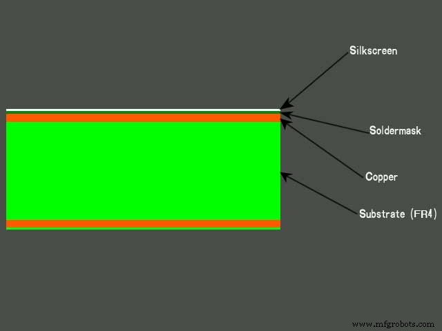
ボード上の文字、数字、記号、画像 (電源のインレットとコンセント、潜在的なマイクロチップの配置、変圧器の位置、プラス + とマイナス - ) などを示すために使用されます。通常、1 色のみが使用され、視認性は一般的に比較的低いです。
その役割は、酸化やほこりや破片などの環境要因がはんだパッドの間に集まるのを防ぐことです。はんだマスクは、はんだブリッジと呼ばれるものを防ぐのにも役立ちます。はんだごての使用中に滑りが発生すると、はんだブリッジが発生し、2 つの導体が接触します。
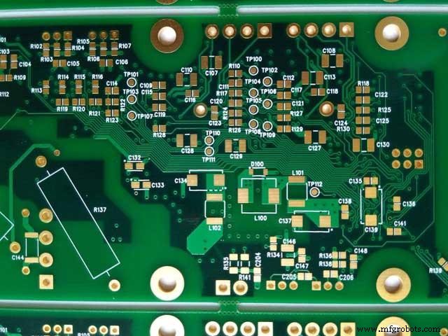
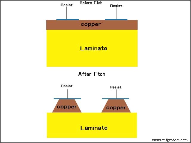
銅は PCB 上の信号経路を示し、目に見える回路パターンは高品質の銅だけが持つ高精度で作られています。 PCB の基板材料とうまく組み合わせると、それを生成できます。
下層の基板であるボード基板は、通常、主にエポキシ樹脂と補強材 (ガラス繊維、時には織布または不織布、さらには紙が使用されている) で構成される誘電体複合材料です。
樹脂には、フィラー状のセラミックを使用することが知られている。最も一般的な基材のタイプは FR -4 (FR は難燃剤の略) です。 FR -4 銅が最高と言える理由は、グラスファイバー基板の中でも際立った優れた導電性を備えているからです。
はい、銅の PCB は、熱抵抗と電気伝導率がはるかに高くなる可能性があります。スーパーコンピューターのブザー用の PCB を使用するという意味ではありません。それは、釣り針や餌を使わずに釣り糸だけで魚を捕まえようとするようなものです。ある失敗。
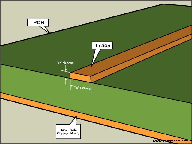
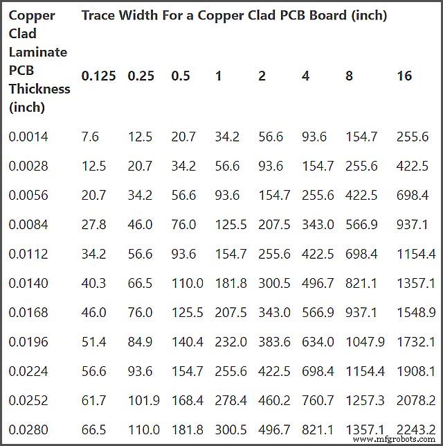
その厚さの標準的な銅の測定単位はオンスです。 (オンス)。ただし、インチで測定できます。ほとんどの場合、PCB に関する銅の厚さは考慮されませんが、1 オンスの銅が平らにプレスされ、1 平方フィートの領域に均一に広がった後の PCB 全体の厚さです。
ほぼすべてのプリント PCB は、1 オンスの厚さの銅で構築されています。 PCB の製造に関しては、メーカーは 1 オンスを想定しています。顧客が特定の仕様を提供しない限り、彼らは設計を引用して構築しています。
ある顧客は、設計には 1 オンスよりも多くの電流を流す必要があると判断しました。その場合、銅の幅またはトレースの幅を増やす方がよいでしょう。場合によっては、完成した銅は 1 オンスです。
通常、2オンス。 1 オンスの銅の厚さは間違いなく最もよく知られた標準的な銅の重量です。銅の厚さは過剰でコストがかかりますが、特に大電流に耐える必要があるグランド プレーンの場合、0.5 銅では不十分な場合があります。
より狭いトレースとスペースが必要な場合は、通常、そうする必要があります。重い銅を必要とする層を複製し、銅を2つに切断したことを確認してください。 8 ミル ラインと 4 オンスの銅線が必要だとすると、レイヤーを複製して 2 オンスを使用するのが最適なオプションです。銅。
重さ5オンスの銅製ウェイトの開始用。以上の場合、より厚い銅の代わりに層を 2 倍にすることもお勧めします。厚い銅の処理の複雑さを考慮すると、厚い銅を使用するよりも層を追加する方が安価です。
ほとんどの顧客が最初に尋ねる質問は、PCB メーカーの BAC-Final-Web-107Minimun ライン幅の機能に基づいています。ただし、ほとんどの場合、銅の重量が答えになることはめったにありません。
|
オンス |
グラム |
ミクロン |
| 1 | 300 | 35 |
| 2 | 600 | 70 |
| 3 | 900 | 105 |
もちろん、ベースレンジは0.5ozから。 3.0オンスまで。同時に、メッキされた銅の範囲は0.7オンスです。 2.0オンスまで。銅の重量が大きいほど、電気的特性が向上し、基板のエッチング プロセスがより複雑になります。
次のような PCB に関する多くのことに影響を与えるため、重量が重要であることを知っておく必要があります。
1.達成可能なトレースとスペース幅の寸法
2. アニュラー リングに推奨される最小幅
3. ベースの銅は、ラインで必要な削減量を決定するため、ベースの銅が等しいほど、ラインの削減が大きくなります。
特に必要な銅の重量が明記されていない場合、PCB の設計段階で多くの注意が払われます。
1.内層で機能しないパッド
2. エッジにトレランスを持たせることでショートを回避できます
3.小穴はマイナス公差を狙う
4. 常に銅の厚さを考慮してください。ほとんどの場合、それはわずか 1 オンスです。銅の。
3.1 重銅の高度な PCB の開発
高度な PCB で重銅を開発する際、多層 PCB は、さまざまなレベルで 2 層から 5 層の銅層を使用して製造されます。同様の銅層を使用して相互接続されているのはどれですか?
追加の銅レベルはボードの機能を強化し、追加のビアはパッドを適切に接続したままにすることで、より多くの電流 PCB を通過させるのに役立ちます。必要なケーブルを所定の位置に維持することで、ボルトを保持する住宅の強度を向上させるのに役立ちます。
新しい低コスト製造法も開発されました。これは、表面から最大 20 マイル離れた重い銅を置き換えることにより、アセンブリに必要な支援を提供します。
重い PCB で使用される埋め込み技術では、基板の表面の上または下に任意の量の銅を含めることができます。
3.2 高電流 PCB と重い銅ベースの基板を組み立てる
大電流の PCB と重い銅ベースの基板を組み立てる場合、開発は困難になる可能性がありますが、余分な時間と労力が必要になるため、不可能ではありません。
このようなボードを開発するには、エンジニアが熱伝達の形で熱の伝達を観察してボードを設計および開発するために特別な注意が必要です。
より良い結果を得るには、十分に高い温度で正しくはんだ付けする必要があります。より高い温度レベルの鉛フリーを使用して PCB を製造することを強くお勧めします。
すべての保持された熱でパッドを取り付けたままにするのに役立つように、適切にラミネートします.
さてPCB。ワンストップサービスと高品質の製品を提供します。必要な書類をお送りいただければ、すぐにお見積りが可能です!私たちは何をぐずぐずしているんですか? 10 年間の PCB 製造は、PCB 製造の初心者または経験者にとって、中国で最も重要な選択肢となっています。この製造に携わる人々は、海外の顧客に不可欠な機能を提供できます。
優先配送業者を選択する優れたオプションを採用することにより。
さてPCB。コスト問題で勢いを増している中国で10年以上のPCB製造を行っています。ワンストップサービスと高品質の製品を提供します。必要な書類をお送りいただければ、すぐにお見積りが可能です!私たちは何をぐずぐずしているんですか?中国で PCB を製造すると、ローカル メーカーの他の地域に比べてコストが低くなるからです。
中国で評判の良いメーカーなので、WellPCBからサービスを受けることができます。彼らは、小規模から大規模の WellPCB まで、顧客にサービスを提供しています。ワンストップサービスと高品質の製品を提供します。必要な書類をお送りいただければ、すぐにお見積りが可能です!私たちは何をぐずぐずしているんですか? 10 年間の PCB 製造があります。
注文するには、ウェブサイトを閲覧し、Gerber ファイルから必要な情報を送信することをお勧めします。
追加料金でカスタマイズされた PCB アセンブリを開発するための優れたオプションをお客様に提供してきた経験があるため、PCB 製造に必要なカスタマイズの種類を指定することをお勧めします。
当社は、お客様が当社に投資したお金の最高の価値を確実に得られるように利用できるリソースを経験しています.
4.カッパークラッド
銅被覆 PCB について語られていないことは何ですか?エンジニアに尋ねて、経済的に安価であることに加えて、否定できないが同等に重要な利点について彼が何度も話しているのを見る必要があります。銅被覆は、PCB を作成する際にほとんどのエンジニアが選択するボードです。
銅被覆 PCB は、作成されているため、回路上にコンポーネントを簡単にはんだ付けできます。コースの設計に最適です。
銅クラッド PCB の材料の競争力により、他のボードと比較してボードのサイズと形状を簡単にカスタマイズできます。材料が利用できるため、他のPCBのコストと比較して電子デバイスの価格が下がります。
銅張 PCB の数多くの用途の中から、いくつかの用途について言及されています。銅被覆 PCB は、武器制御システム、レーダー システムに供給される電力、高出力平面変圧器の 1 次および 2 次巻線、配電盤、バッテリー充電器および監視システムで一般的に使用されます。
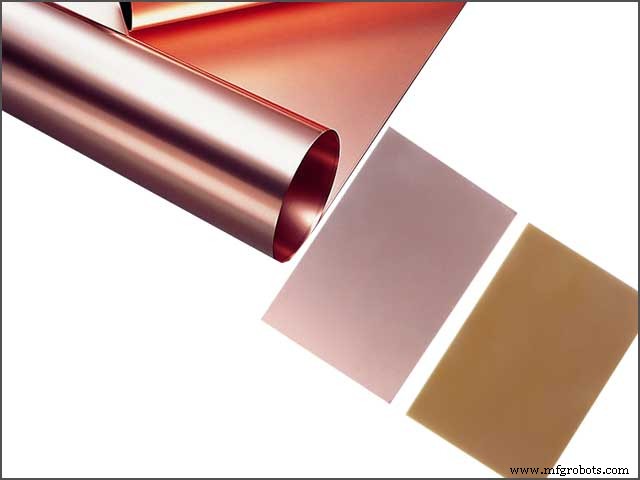
4.1 銅 PCB —コッパー クラッド ラミネート:
CCL(Copper Clad Laminate)と略され、木材パルプ紙やガラス繊維を樹脂や補強材に浸した基材を指します。
CCL は次のように分類できます:
- 1.機械的剛性に基づく CCL – このタイプの CCL は剛性です
- 2.有機樹脂による絶縁をベースとしたCCL
- 3.厚さに基づく CCL は、通常約 0.55 mm です
- 4.絶縁樹脂CCL.
さまざまな種類の CCL があります
それらは、機械的剛性、断熱材、厚さ、および補強材の種類に基づいて、さまざまな分類基準に従って分類されます。
- 1.機械的剛性による: リジッド CCL (G10、FR-4、CEM -1) とフレックス CCL があります。リジッド PCB はリジッド CCL に依存し、フレックス PCB はフレックス CCL に依存します。
- 2.断熱材別: 有機樹脂CCL、金属ベースCCL、セラミックベースCCLなど多数あります
- 3.厚さ別: 標準の厚い CCL と薄い CCL があります。厚い CCL には 0.5 mm を超える厚さが必要であり、薄い CCL には 0.5 mm 未満の厚さが必要です
- 4.強化素材別: ガラス繊維ベース (FR -4)、紙ベース (XPC)、コンパウンド CCL (CEM -1、CEM -3) があります。
- 5.適用された絶縁樹脂による: We have epoxy resin CCL (FR -4, CEM -3) and phenolic CCL (FR -1, XPC).
4.2 Copper PCB —Quick Question:What Makes An Excellent CCL?
Simple, an excellent CCL needs to meet specific requirements to be called EXCELLENT, which includes
♦ Appearance:
do you like dents and scratches in your car? Guessing no, well same for CCL; a cut, gash, wrinkle, or pinholes can lead to low performance in the CCL and turn the PCB. So the smoother and cleaner the job, the better the performance.
♦ Size:
Your CCL is a base material for the PCB; it needs to conform to the size requirement of the PCB.
♦ Electrical Performance:
this is the primary mission of the CCL which means it’s the primary mission of the PCB; specific details have to be paid to the Volume Resistance, Insulation Resistance, Dielectric constant, Arc resistance, and so on.
♦ Physical Performance:
In physical performance, it’s always noteworthy to consider the bending strength, thermal stress, heat resistance, and punching quality.
♦ Chemical Performance:
The requirements needed to be met by the CCL are flammability, dimension stability.
♦ Environment Performance:
The CCL should meet water absorption standards.
Within the CCL is what we call a prepreg, which is reinforced material; it is the reinforcement material used in a CCL. It is made of fiber and is referred to as the bonding sheet. It is mainly made of fiber cloth, epoxy resin, acetone, and many others.
Using quality prepreg results in high-quality CCLs, which enhances the quality of PCB. The quality of the prepreg material used depends on the resin content, resin fluidity, and dicyandiamide crystallization. Consequently, you should select resin based on the quality and the cost.
The cost should be related to the thickness of the fiber cloth. Thinner prepreg is recommended even though it might be a little bit costly.
To meet Restriction of Hazardous Substances Regulations, it is recommended that you look at the reliability and heat resistance of the CCls. The latest CCL has been enhanced by modifying them so that they:
Include Halogen-free CCL – refers to CCL with the content of bromine and chlorine controlled within 900ppm. Care should be taken so that the content does not exceed 1500ppm.
Lead-free CCL – refers to Copper laminate with surface mounting that has been carried out without applying lead-free solder. The epoxy resin may be used, but the RoHS regulations must be adhered to. Note that RoHS prohibits the use of substances such as PBDE and PBBD substances.
4.3 Classification Of Resin
Resins used in CCls could be classified as:
- Epoxy resin
- Phenolic resin
- Polyamide resin
- Bismaleimide triazine
- Phenolic resin
If you are using fiber, the following quality aspects should be considered:
- Humidity resistance
- Intensity
- Insulation capability
- Heat and fire resistance
4.4 Copper PCB —Copper Laminates
This is the used clad that is over the dielectric layer and substrate (resin composite material).
The copper acts as a composite insulator material while being a good conductor, also remember. You can have rigid or flexible base material. Still, the primary purpose of the copper laminate is to act as mechanical support for the pin, i.e., the firm base that holds the electronic component and joins them at the same time.
The most popular types of copper laminates used for PCB are:
♦Polyimide:
This is a base material used for high-temperature PCB applications; it has an excellent glass transition (Tg =220 °C) that gives it an outstanding performance over high temperatures. It allows for soldering and desoldering of components, giving you more legroom for mistakes.
♦Phenolic:
This base material is used in low-cost applications with the FR-2, CEM-1, or CEM-3 brand names. It is most widely used in single-layer PCB of small household gadgets and appliances. It is slightly brittle but hard to bend.
♦Arlon:
So far, it’s one of the most devise base materials with different applications just behind the FR -4; it is the preferred base material for multilayer PCBs; you find them in military, wireless, and communication systems.
♦FR-4:
This is a glass fiber base material that is durable, hard to bend, and cut with fire retardant qualities; it’s Tg =160°C. Because of all these qualities, various applications within single, double, and multilayer PCBs are used for power supply, mixed-signal and digital applications.
Other Copper Laminates used are Tetrafunctional epoxy, Thermount, and cyanate ester.
For electrically interconnecting the components, the laminates can be nickel, stainless steel, aluminum, and copper. However, the most widely used material for lamination purposes is copper. The aluminum found commercial applications recently and is appreciated in low-cost home appliances.
The conductive cladding layer is skinny and is over one or both sides of the resin composite material. The thickness of the cladding material is determined by how much material is deposited regarding weight.
It is a simple process but requires that you take some precautions. First, you need to turn the laminator on before feeding the board and the film in the machine. The side with the excess border should be provided into the laminator.
In most cases, you are required to put the board into the machine for the second time if you want to improve the quality of your clad board. It means that the board should be put back into the laminator immediately after it finishes the first run.
The same procedure should be used if you are working on a double-sided board.
5. Copper PCB —Copper Layer Design
A keen eye is kept by designers when designing copper PCB; a designer must think in reverse. A board starts as solid copper; then, you remove the bits you don’t want.
It is faster to build, less expensive, and consuming when the copper is the same size as the board. Some techniques can make much difference from a frustrating experience to a smooth experience.
Maximizing copper is most common in two ways:
• Manually:
By specifying the specs of your PCBs (shape and size), this method is faster but sloppy as copper can be placed as an object, and these objects are checked for minor errors when assigned to a net. This method is mainly used for quick turns or prototype builds.
• Automatically:
However, this method is more time-consuming than the manual process, but the pour method helps to maximize copper. Copper will be left behind by drawing a border around the board area and pouring the copper in, laying out the board, and going back and placing copper shapes to fill it.
What you need to know is that when the copper pour is used, you define your boundary and everything inside when the pour operation is performed while connected automatically.
This method usually favors a large area, several irregularly shaped objects, or unusual shapes. The pour operation automatically fills the unique body while additionally isolating other traces in the area.
Objects that the copper pour can automatically handle are Traces, nets, decals, and pads. When used right, you don’t need much; the copper pouring will make the right moves and connections; you can double-check using the continuity check tool.
Now we have talked about both the manual and automatic methods, and you probably think the manual process is the best, especially for the short time sprint. Still, in the long run, the intuitive approach can be better even though it is works upfront.
There are three situations when using a copper pour might be the better option for your design.
1. Polygon Management
Manual – when you’re dealing with regular polygons, this method could be time-consuming and messy. A quick fix would be to drop overlapping shapes on top of each other to build your required profile.
It is quick, but it’s a short-term solution as eventually, you will need to do vertex editing to clean the design.
Automatic – The copper pouring method here is a “no-brainer” because we deal with complex shapes; this process is automatic. By defining the border and running copper, you eliminate the tedious job of re-editing later.
2. Plane Management
Manual – A plane is a large area of copper where all connections are one net. If you intend to build a board with separate planes while changing parts often, you often recommend route traces point to point.
Automatic – An excellent way to avoid several traces that all go to the same point is to use a copper pour method design on a plane for the ground. This will automatically connect all the connections on one network.
3. Thermal Management
Manual – if you have a Hot board with much space, the best way to cool it down is to add a copper square to help conduct the heat away. Which may not always be the case?
Automatic – when you define the area around the critical parts of the board, prioritizing them, you can minimize the thermal stress. This method is used when importance is placed on maximizing the copper surface area.
6. PCB Copper Plating And Cleaning
6.1 Copper PCB —Plating
Plating is very important to a PCB board. If all the traces on the external layers are not protected, the copper PCB will oxidize and deteriorate, making the board unstable. How do you know your copper has corroded? It will turn green. The two main reasons for plating are also called copper coating and surface finish:
1. To protect exposed copper circuitry
2. To provide a surface good enough for soldering when assembling components to the PCB.
You have various PCB copper plating options to choose from, and each carries its advantages and disadvantages. You can find them here.
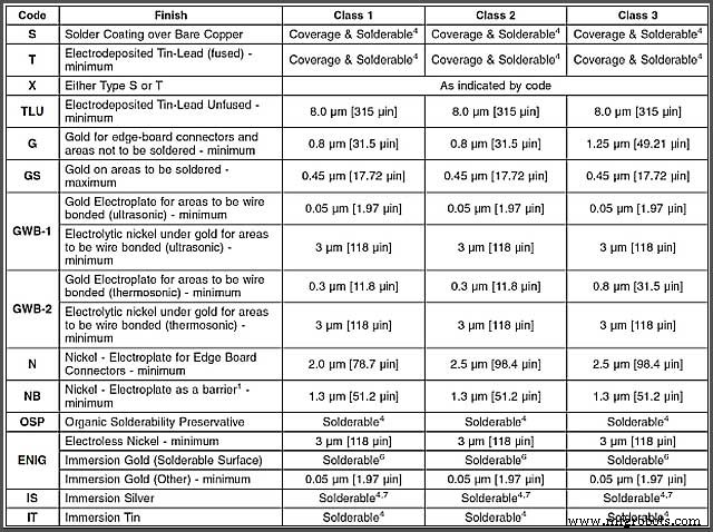
There are IPC standards for surface plating which is shown below:
6.2 Copper PCB —Clad Board Cleaning
Getting the best results is essential for you to clean your board using fine wool. You may also choose to use an abrasive pad before rinsing it with water. It helps to remove the dirt and any other contamination.
Alternatively, you may start by cleaning the dry board by exposing it to heat for about 5 minutes. This way, it ensures that the board is clean and ready for the film.
Conclusion
But I can answer you with one sentence “Copper PCB is the most reliable, effective PCB used across the most electronic device,” you don’t need to take my word for it. Just take a look at your phones.
And we at WellPCB are here to meet your needs at any time.