


スリーステートエレクトロクロミックデバイスのディップコーティングプロセスエンジニアリングと性能最適化
要約
二酸化チタン(TiO 2 )ナノ粒子は、さまざまなナノ粒子サイズ、持ち上げ速度、前駆体濃度、および浸漬数を使用したディップコーティング技術によって、フッ素ドープ酸化スズ(FTO)に修飾されました。続いて、修飾されたFTO電極と平坦なFTO電極の間に適切な量のゲル電解質を挟むことにより、可逆的な3状態光学変換(透明、ミラー、および黒)を備えた電着ベースのエレクトロクロミックデバイスを製造しました。ディップコーティングプロセスエンジニアリングとTiO 2 の形態的特徴との相関関係 薄膜、すなわち、厚さおよび粗さ、ならびにエレクトロクロミックデバイスの性能、すなわち、光学的コントラスト、スイッチング時間、およびサイクル安定性を調査した。変更されたデバイスは、57%の高い光学コントラスト、6秒と20秒の短い着色/漂白スイッチング時間、およびディップコーティングプロセスエンジニアリングを調整することにより、わずか27%の減少率の1500サイクル後の優れたサイクル安定性を示します。この研究の結果は、満足のいく性能を備えたエレクトロクロミックデバイスの合理的設計のための貴重なガイダンスを提供します。
背景
エレクトロクロミック材料の魅力的な特徴は、電圧を印加したときに可逆的かつ持続的に光学特性を変化させる能力です。 Deb [1]の先駆的な研究以来、さまざまなエレクトロクロミック材料が開発されており、遷移金属酸化物[2]、プルシアンブルー[3]、導電性ポリマー[4]、ビオロゲン[5]などのいくつかのサブセットに分類できます。 、遷移金属イオン配位化合物[6]、ハイブリッドエレクトロクロミック材料[7]、および可逆電着ベースのエレクトロクロミック材料[8、9]。光学コントラスト、スイッチング時間、着色効率、サイクリング安定性、光学メモリー効果などのエレクトロクロミック性能が広く研究されており、スマートウィンドウ、アンチグレアバックミラー、エレクトロクロミックディスプレイ、電子紙、および軍事カモフラージュ[10、11、12、13、14、15、16、17、18、19]。可逆電着に基づくエレクトロクロミックデバイスは、そのシンプルなサンドイッチタイプの構造と簡単で低コストの製造により、光変調への応用が期待されています。それらの光学特性は、印加電圧および溶解下での透明導電性電極への金属(銅(Cu)、ビスマス(Bi)、鉛(Pb)、ニッケル(Ni)、銀(Ag)など)の堆積によって操作できます。電圧を除去すると、金属が電解質に戻ります[20、21、22、23、24、25、26]。ビスマス-銅(Bi / Cu)電着デバイスは、BiとBi 3+ の間の酸化還元によって可能になる、黒と透明の状態の間の迅速で可逆的な切り替えにより、情報ディスプレイで広く使用されています。 [9、23、24、25]。同様に、Agベースの電着システム[26,27,28,29]も、ミラー状態を実現する能力のためにエレクトロクロミックデバイスを製造するために開発されました。
通常、適切な電極表面修飾は、修飾された電極表面の光の吸収および/または多重散乱のために、電着ベースのエレクトロクロミックデバイスの可逆的で複数の色の状態を引き起こす可能性があります[30、31、32、33]。エレクトロクロミック薄膜の製造には、スパッタリング[34]、真空蒸着[35]、化学蒸着[36]、熱水[37]、電着[38]、ゾルゲル[39、40]などのさまざまな技術が利用されてきました。 。さまざまな技術の中で、ゾルゲルアプローチは、その低コスト、大面積の準備に適している、および扱いやすい特性のために有利であり、その中でスピンコーティングおよびディップコーティング技術が広く使用されている。スピンコーティングと比較して、ディップコーティング技術は、その高い制御性と大規模な調製により適しているため、好まれます[24]。さらに、Deepa etal。 [24]はまた、三酸化タングステン(WO 3 )薄膜は、改善された伝送変調、着色効率、スイッチング速度、着色/漂白サイクルなど、スピンコーティングされたデバイスと比較して優れた性能を示しました。ただし、ディップコーティング技術は、電着ベースのAg / Cuエレクトロクロミックデバイスの製造にはまだ適用されていません。
基本的に、エレクトロクロミック材料のエレクトロクロミック性能(すなわち、光学的コントラスト、スイッチング時間、着色効率、サイクル安定性、および光学的メモリー効果)は、基本的にそれらの構造的、表面形態学的、および組成的特性に依存します[41]。したがって、エレクトロクロミック材料の特性を改善するために、調製パラメータを綿密に検査することが非常に必要です。 Deepa etal。 [42]製造されたWO 3 ディップコーティング技術によるフィルム、およびシュウ酸塩アセチル化ペルオキソタングステン酸ゾルからの薄膜堆積中の相対湿度(RH)変化(55および75%RH)がWO 3 アニーリング時に得られたフィルムが提示された。クリア状態とブルー状態の間のより速いスイッチング速度、リチウムインターカレーションのより大きな電流密度、リチウムのより高い拡散係数、および優れたサイクル安定性が、75%RHで製造されたフィルムによって得られ、湿度変化の影響を示しています。エレクトロクロミック材料の構造とエレクトロクロミック特性。サンと彼の同僚[43]はWO 3 を準備しました スピンコーティング法と組み合わせたゾルゲル法による薄膜。 WO 3 の微細構造と光学特性に及ぼすアニーリング温度の影響 フィルムを調査し、より低いアニーリング温度で可視範囲でより高い透過率変調が得られました。前駆体ゾル中の有機部分のタイプと含有量、フィルム調製法(スピンコーティングまたはディップコーティング)がフィルム特性に及ぼす影響も広く調査されており[43、44]、エレクトロクロミック性能とエレクトロクロミック薄膜の製造パラメータ。荒木ほか[41]スピンコーティングを介して修飾インジウムスズ酸化物(ITO)電極上にAgを堆積させ、可逆的な黒色および鏡面状態を得た。ツボイと彼の同僚[42、44]は、異なる電圧下でのAg粒子の成長を制御することにより、複数の色状態のさらなる追求も行っており、ナノ粒子のサイズと形状の操作が劇的な変化をもたらす可能性があることを示しています色で。以前の研究[33]では、導電性TiO 2 を使用して、可逆的な3状態光学変換(透明、黒色、およびミラー状態)を備えた電着ベースのAg / Cuエレクトロクロミックデバイスを製造しました。 スピンコーティング技術によって製造されたナノ粒子修飾フッ素ドープ酸化スズ(FTO)電極。また、TiO 2 の表面構造を操作することにより、さまざまな状態のデバイスの光学特性を効果的に制御できることも実証しました。 -変更されたFTO電極。ただし、マルチステートエレクトロクロミックデバイスに対する電極表面改質の影響の詳細な検査はほとんど報告されていません。したがって、製造パラメータを通じて電着ベースのエレクトロクロミックデバイスの特性を徹底的に調査することは重要です。
この研究では、TiO 2 ナノ粒子は、ディップコーティング技術によってFTOに修飾され、続いて、修飾されたFTO電極と平坦なFTO電極の間に適切な量のゲル電解質を挟み、可逆的なスリーステート光変換を備えた電着ベースのエレクトロクロミックデバイスを製造しました。ディップコーティング技術の高い可制御性のために、デバイスの光学性能は、電極表面の変更を操作することによって調整することができます。ナノ粒子のサイズは、操作できる重要なパラメータであり、製造されたデバイスの性能を変える可能性があります。したがって、ナノ粒子のサイズを調整して、TiO 2 の微細構造への影響を調査します。 薄膜と製造されたデバイスの性能。ナノ粒子のサイズを除いて、リフティング速度、前駆体濃度、および浸漬数は、浸漬コーティングプロセス中の主なパラメータです。ここでは、持ち上げ速度、前駆体濃度、および浸漬数も変化させて、TiO 2 の微細構造への影響を調査しました。 薄膜、およびエレクトロクロミックデバイスの性能、すなわち、透過率/反射率、光学コントラスト、スイッチング時間、およびサイクル安定性。この研究の結果は、満足のいく性能を備えたエレクトロクロミックデバイスの合理的設計のための貴重なガイダンスを提供します。
メソッド
資料
サイズ25×30mm、厚さ2.2 mm、シート抵抗10Ωsq -1 のFTO透明導電性ガラス 電極として使用し、武漢ラティスソーラーエナジーテクノロジー株式会社から購入しました。均一なTiO 2 FTO電極の修飾には、平均直径が5〜10、40、100 nmのナノ粒子(Aladdin Co. Ltd.)を使用しました。ジメチルスルホキシド(DMSO、≥99.8%、J&K Chemical Co.Ltd。)、テトラ- n を含む電解質化合物 -臭化ブチルアンモニウム(TBABr、99%以上、J&K Chemical Co.Ltd。)、硝酸銀(AgNO 3 、≥99.8%、Guangdong Guanghua Sci-Tech Co.Ltd。)、塩化銅(CuCl 2 、≥99.0%、KeLong Chemical Co.Ltd。)、ポリ(ビニルブチラール)(PVB、Sekisui Chemical Co.Ltd。)、エチルセルロース(≥99.5%、Hanzhou Lanbo Industrial Co.Ltd。)、ラウリン酸(≥99.8 %、KeLong Chemical Co.Ltd。)、テルピネオール(≥98.0%、KeLong Chemical Co.Ltd。)、およびエチルアルコール(≥99.7%、KeLong Chemical Co. Ltd.)は商業的供給源から入手した。すべての溶媒と化学物質は試薬品質であり、さらに精製することなく使用されました。厚さ0.5mmのテフロンシート(Aladdin Co. Ltd.)を20×20mmの穴で25×25mmにカットしました。 FTOガラス電極とテフロンシートの両方を、使用前にエタノールと脱イオン水で数回洗浄しました。
TiO 2 の準備 ナノ粒子分散液とゲル電解質
TiO 2 を準備するには ナノ粒子分散液、TiO 2 ラウリン酸(界面活性剤、0.25 g)とエチルセルロース(接着剤、0.75 g)を含むナノ粒子(原材料、2.5 g)を最初にボールミルジャーに入れ、テルピネオール(接着剤、16 mL)とエチルアルコール(接着剤、16 mL)と混合しました。溶媒、10 mL)粉砕直前。 TiO 2 ナノ粒子スラリーは、50分間の粉砕後、エチルアルコールで希釈して得られました。ゲル電解質を調製するために、TBABr(806 mg、2.5 mmol)、硝酸銀(85 mg、0.5 mmol)、および塩化銅(13 mg、0.1 mmol)を10 mLのDMSOに溶解し、続いてPVB( 1.32 g、10 wt%)。最後に、混合溶液を24〜48時間暗所に置いて、ゲル電解質を得ました。
FTO電極の変更とエレクトロクロミックデバイスの製造
ディップコーティング技術を使用して、FTO透明導電性電極を変更しました。一般的なプロセスは次のとおりです。希釈剤としてのエチルアルコール(10、15、または20 mL)をTiO 2 に追加しました。 ナノ粒子分散液(5 mL)、30分間超音波混合。続いて、背面全体と前面上部にタップを貼り付けたFTO電極をディップコーターに固定し、前述の分散液に6000 µm / sの速度で浸漬し、1000、2000、3000 µm / sの速度で持ち上げました。 、 それぞれ。 TiO 2 ナノ粒子で修飾されたFTO導電性電極は、調製したままのサンプルを500°Cで30分間焼結することによって得られました。比較のために、TiO 2 さまざまなサイズ(5〜10、40、および100 nm)のナノ粒子が使用され、リフト速度(1000、2000、および3000μm/ s)、前駆体濃度(TiO の比率)など、ディップコーティングのさまざまなパラメーターが使用されました。 2 この研究では、ナノ粒子分散液と1:2、1:3、および1:4)のエチルアルコール、および浸漬数(1、3、および5)を使用しました。具体的には、TiO 2 の影響を調査します。 エレクトロクロミックデバイス、TiO 2 の性能に関するナノ粒子サイズ リフティング速度を3000μm/ s、プリカーサー濃度を1:2、ディッピング数を1に固定して、サイズが5〜10、40、100nmのナノ粒子を使用しました。リフティングの影響を調査するため。エレクトロクロミックデバイスの性能の速度、1000、2000、および3000μm/ sの持ち上げ速度は、TiO 2 を固定することによって使用されました。 ナノ粒子サイズは5〜10 nm、前駆体濃度は1:2、浸漬数は1です。エレクトロクロミックデバイスの性能に対する前駆体濃度の影響を調べるために、TiO 2 の比率 ナノ粒子分散液と1:2、1:3、1:4のエチルアルコールをTiO 2 を固定して使用しました。 ナノ粒子サイズは5〜10 nm、リフト速度は3000 µm / s、浸漬数は1です。エレクトロクロミックデバイスの性能に対する浸漬数の影響を調べるために、浸漬数1、3、および5はTiO 2 を固定することによって使用されます ナノ粒子サイズは5〜10 nm、持ち上げ速度は3000 µm / s、前駆体濃度は1:2です。電着ベースのエレクトロクロミックデバイスを組み立てるために、DMSOベースのゲル電解質を20mm×20mmの密閉された正方形のスペースに入れ、0.5 mmの厚さのテフロンシートの内側にカットし、2つのFTO電極の間にテフロンシートを挟んで密封しました(そのうちの1つはTiO 2 で修飾されています ナノ粒子)。
特性評価
電界放出型走査電子顕微鏡(FESEM、S-3400、日立)を使用して、TiO 2 の形態を観察しました。 ナノ粒子修飾FTO電極。 TiO 2 の粗さ ナノ粒子修飾FTO電極は、原子間力顕微鏡(AFM、マルチモードV、Veeco)を使用して特性評価されました。電気化学ワークステーション(CHI660D、CHI)を使用してエレクトロクロミックデバイスに変換電圧を印加し、UV-Vis分光光度計(Cary 5000、Agilent)を使用して透過率と反射率のスペクトルを測定しました。光学的コントラスト、スイッチング時間、サイクリング安定性を含むすべてのエレクトロクロミック特性は、2電極モードを使用して得られました。負極と正極はフラットFTO電極とTiO 2 に接続されています。 それぞれ、ナノ粒子で修飾されたFTO電極。測定中のエレクトロクロミックデバイスの対電極はフラットFTO電極であり、作用電極はTiO 2 でした。 ナノ粒子修飾FTO電極。適切な電圧を印加することにより、ディップコーティングされたエレクトロクロミックデバイスは、透明、ミラー、および黒を含む3つの可逆的な光学状態を示しました。
結果と考察
電鋳ベースの電鋳デバイスに適切な電圧を交互に印加/除去することにより、ミラー状態、ブラック状態、および透明状態の間の可逆的なスリーステート光学変換を実現できます。黒とミラーの状態は、粗いTiO 2 に堆積したAgに対してトリガーされます。 それぞれナノ粒子修飾FTO電極とフラット電極。したがって、変更されたデバイスの黒色状態は、それらの表面形態学的構造によって強く影響を受ける可能性がある。 TiO 2 の表面形態構造の影響を調査する 変更されたデバイスの性能に関する薄膜、TiO 2 を含む3つの前駆体溶液 さまざまなサイズ(5〜10、40、および100 nm)のナノ粒子をボールミルで調製しました。続いて、ディップコーティング技術、焼結処理、および修飾FTO電極と平坦なFTO電極との間に適切な量のゲル電解質を挟むことにより、FTO電極の表面に前駆体溶液をコーティングすることにより、修飾デバイスが得られた。まず、透明、ミラー、黒の状態にある3つの変更されたデバイスの光透過率と反射率のスペクトルを、400〜800nmのスペクトル領域で測定しました。透過率測定では、電源の負極と正極をフラットFTO電極とTiO 2 に接続しました。 ナノ粒子で修飾されたFTO電極は、それぞれ+2.5 Vのミラー状態と、20秒後に-2.5Vの黒色状態になります。反射率測定では、同じ電圧を90秒間印加しました。透明な状態では、TiO 2 で調製された改良型デバイスで61、50、および46%の透過率が観察されます。 それぞれ5〜10、40、100 nmのナノ粒子(図1a〜c)。黒の状態では、変更されたデバイスはTiO 2 で作成されています 5〜10 nmのナノ粒子は、最大透過率が15%で、TiO 2 のサイズを大きくすると10%に減少します。 100 nmまでのナノ粒子(図1a–c)。ミラー状態では、変更されたデバイスはTiO 2 5〜10 nmのナノ粒子は、40および100 nmのナノ粒子と同様の透過率を示します(図1a〜c)。光学コントラストは通常、エレクトロクロミックデバイスの着色プロセスと漂白プロセスの間の透過率、反射率、または吸光度の最大差として定義されます。透明状態と黒色状態の間のデバイスの透過率の差を計算することにより、48、42、および39%の光学コントラストが得られます。 TiO 2 の増加に伴う光学コントラストの低下 ナノ粒子のサイズは、主に透明な状態のデバイスの透過率の低下に起因します。 5〜10 nm TiO 2 で調製された改良型デバイスの反射率ピーク ナノ粒子は、40および100nmのTiO 2 で調製されたものとは異なります。 ナノ粒子。ピーク位置はそれぞれ700、750、750 nmです(図1d–f)。基本的に、屈折率は通常、材料、構造(すなわち、膜の数と配置)、厚さ、および膜の界面形態/構造によって決定されます。したがって、ミラー状態の修正電着ベースのエレクトロクロミックデバイスの波長依存反射スペクトルにおけるこのピークシフトの理由は、変化したTiO 2 の複合効果である可能性があります。 ナノ粒子サイズ、TiO 2 薄膜の厚さ、およびTiO 2 薄膜表面粗さ[45,46,47]。さらに、ミラー状態の変更されたデバイスでは70%を超える反射率が観察され、黒とミラー状態の3つの変更されたデバイスでは20%の低い反射率が観察されます(図1d–f)。上記の値は、到達可能な最も暗い状態に対応していないことに注意してください。前述の結果は、電鋳ベースのデバイスの光透過率、光反射率、および光学コントラストが、TiO 2 のサイズによって変化する可能性があることを示唆しています。 透明電極上に堆積したナノ粒子。
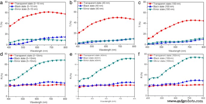
(オンラインカラー)透明(赤)の電鋳ベースの電鋳デバイスの光学特性 )、黒(青 )、およびミラー状態(緑 )。 a で作成された変更されたデバイスの透過率スペクトル 5〜10、 b 40、および c それぞれ100nm。 d で作成された変更されたデバイスの反射スペクトル 5〜10、 e 40、および f それぞれ100nm
ディップコーティングされたTiO 2 の構造的特徴 異なるナノ粒子サイズの薄膜を調査した。焼結ディップコーティングされたTiO 2 のX線回折(XRD)パターン フィルム、準備されたままのディップコーティングされたTiO 2 フィルム、新鮮なTiO 2 さらに処理せずにナノ粒子を処理し、禿げたFTO透明導電性電極を2 θに記録します。 20°から80°の範囲です[33、48]。追加ファイル1:図S1aに示されているように、調製されたままのTiO 2 の回折ピーク フィルム、焼結TiO 2 フィルム、および新鮮な5〜10 nm TiO 2 さらに処理されていないナノ粒子は同じ位置で発生し、アナターゼ構造のTiO 2 と非常によく一致します。 (TiO 2 アナターゼ、JCPDS 21-1217)。これらの値は文献データ[48]とよく一致しており、アナターゼ相の結晶面(101)、(004)、(200)、(105)、(211)、および(204)に対応して分散ピークが広がっています。 。 52°と62°で観察された余分なピークはFTO電極表面に由来し、酸化スズ(SnO 2 )の構造形態とよく一致します。 、JCPDS 46-1088)[33、49]。同様のアナターゼ構造は、40および100nmのTiO 2 でも観察されます。 焼結前後のナノ粒子修飾FTO電極(追加ファイル1:図S1bおよびS1c)。ディップコーティングされたTiO 2 薄膜は、新鮮なTiO 2 と同じ構造形態のままです。 FTO電極を変更するための製造手順全体を通してナノ粒子。これは、コーティングされたTiO 2 の構造的特徴を示しています。 薄膜はディップコーティング法の影響を受けず、以前のレポート[33]でも同様の結果が示されています。
第二に、3つのディップコーティングされたTiO 2 の形態的特徴 薄膜を調べた。ディップコーティングされたTiO 2 の写真、面内および断面SEM画像 図2に、Ag堆積前の薄膜を示しました。TiO 2 で堆積したFTO電極 ナノ粒子は異なる透明度を示し、TiO 2 のサイズを大きくすると徐々にぼやけます。 ナノ粒子(図2a–c)。 TiO 2 で作成された薄膜 5〜10 nmのナノ粒子は、粒子間にシャープで明確な境界があり、細孔と粒子が均一に分布していることを示しています。これは、均質で微細なTiO 2 を示しています。 得られた薄膜(図2d)。 TiO 2 のサイズを大きくした後 ナノ粒子、堆積したTiO 2 の表面 ただし、薄膜は粗く不均一になります(図2e、f)。 TiO 2 のこの不均一な分布 ナノ粒子は主に、エチルアルコールの分散度が徐々に低下し、ディップコーティングおよび焼結プロセス中に凝集することから生じます。徐々にぼやけて粗いTiO 2 ナノ粒子のサイズが大きくなる薄膜は、図1aに示すように、変更されたデバイスの透過率スペクトルが減少していることを示しています。通常、3つのTiO 2 の厚さの増加 薄膜は、TiO 2 の厚さで断面SEM画像を介して測定されます 5〜10、40、および100nmのTiO 2 で調製されたFTO電極用の320、409、および612nmの薄膜 それぞれ観察されたナノ粒子。ディップコーティング工程では、溶媒蒸発工程での粒子重力、揚力、毛細管力のバランスにより、連続薄膜が得られます。さまざまな粒子重力と毛細管力から生じるさまざまなバランス力が、さまざまなナノ粒子サイズで予想され、さまざまな厚さと粗さにつながります。図1a、bに示すように、透明状態の変更されたデバイスの透過率、反射率、および光学コントラストは、TiO 2 を増やすと変化します。 ナノ粒子サイズ。したがって、拡大されたTiO 2 の場合、透明状態での修飾エレクトロクロミックデバイスの光透過率の低下が見られます。 ナノ粒子のサイズは、主にディップコーティングされたTiO 2 の厚さの増加によって説明できます。 薄膜。
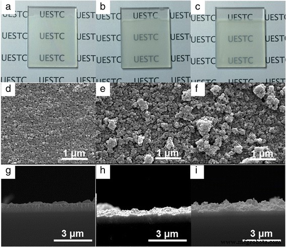
(オンラインカラー)TiO 2 の写真 a のナノ粒子サイズで作成された薄膜 5〜10、 b 40、および c それぞれ100nm。 TiO 2 の面内SEM画像 d のナノ粒子サイズで作成された薄膜 5〜10、 e 40、および f それぞれ100nm。 TiO 2 の断面SEM画像 g のナノ粒子サイズで作成された薄膜 5〜10、 h 40、および i それぞれ100nm
3つのディップコーティングされたTiO 2 の粗さ 図3a–cに示すように、原子間力顕微鏡(AFM)を使用して薄膜をさらに測定しました。ディップコーティングされたTiO 2 の粗さ ナノ粒子サイズの関数としての薄膜が図3dにプロットされており、TiO 2 の粗さは39、117、142nmです。 5〜10、40、および100nmのTiO 2 で作成された薄膜 それぞれ測定されたナノ粒子。より大きなTiO 2 の場合、より多くの凝集とより低い分散度の結果として、粗さの増加が観察されます。 ナノ粒子。基本的に、透過率と関連する反射率は、デバイスに入射する波の振る舞いを説明するために使用されます。必須の指標である屈折率係数は、材料、構造(つまり、膜の数と配置)、厚さ、および膜の界面形態/構造によって決定されます。異なるサイズのTiO 2 を備えた修正電着ベースのエレクトロクロミックデバイスの光学特性を調査する際には、前述のすべての要因を考慮に入れる必要があります。 ナノ粒子。変更されたデバイスの黒色状態をトリガーした後、すべてのFTO表面が暗黒に変わり、Ag層がFTO電極の表面形態を大幅に変更したことを示します(追加ファイル1:図S2a、S2b、およびS2c)。 Ag層が堆積した修飾デバイスのすべてのFTO表面は、禿げたTiO 2 でコーティングされたデバイスよりも滑らかになります。 薄膜(追加ファイル1:図S2d、S2e、およびS2f)。ディップコーティングされたTiO 2 の断面SEM画像 薄膜(追加ファイル1:図S2g、S2h、およびS2i)も、3つの変更されたデバイスすべてに対して厚くてコンパクトなAg堆積層を示します。図1に示すように、透過率と反射率のスペクトルはAgの堆積後に変化し、デバイスは黒色の状態に変化します。これは、透過率と反射率に対する厚さと粗さの強い影響を示しています。追加の堆積Ag層、変更された厚さ、最上層の界面形態など、変更された膜構造の複合効果を考慮する必要があります。
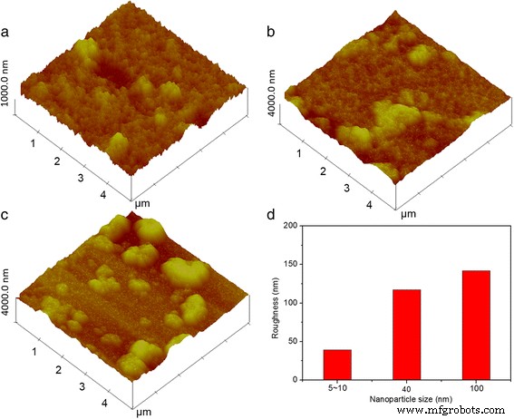
(オンラインカラー)TiO 2 のAFM画像 a のナノ粒子サイズで作成された薄膜 5〜10、 b 40、および c 100nmおよび d TiO 2 の粗さ TiO 2 の関数としての薄膜 ナノ粒子サイズ
第3に、700 nmでの3つの変更されたデバイスの時間依存透過率の変化が、2電極サイクリックボルタモグラム(CV)テスト中に、4つの連続した着色/漂白サイクルと100 mV / sの掃引速度で測定されました。透過率測定では、+ 2.5Vと-2.5Vの電圧を交互にTiO 2 に印加しました。 -20秒間FTO電極を変更しました。図4は、TiO 2 で作成された改良型デバイスの透過率の経時変化を示しています。 さまざまなサイズのナノ粒子。 5〜10、40、および100nmのTiO 2 で作成された変更されたデバイスの初期透過率 ナノ粒子は、漂白すると61、50、46%に達し、着色するとそれぞれ34、25、18%に低下します。基本的に、着色プロセスはデバイスが透明状態からミラー/ブラック状態に変化することを意味し、ブリーチプロセスはデバイスがミラー/ブラック状態から透明状態に逆に変化することを意味します。着色/漂白の切り替え時間は、着色および漂白プロセス中に最大変調の90%に達するのに必要な時間として表されます。 TiO 2 で変更されたデバイスについて、さまざまなスイッチング時間が測定されました。 さまざまなサイズのナノ粒子、5〜10nmのTiO 2 で調製された改良型デバイス ナノ粒子は、着色プロセスと漂白プロセスの間で最短の切り替え時間(着色の場合は6秒、漂白の場合は20秒)を示します。ナノ粒子サイズの増加に伴うスイッチング時間の増加は、FTO電極がより薄くより滑らかなTiO 2 で修飾されていることを示しています。 薄膜は、着色/漂白の切り替え時間を短縮するのに役立ちます。さらに、漂白プロセスは、すべてのデバイスの着色プロセスよりも遅くなります。これは、エレクトロクロミックデバイスに関するほとんどの記事で説明されています。さらに、変更されたデバイスが透明からミラー状態に変化する時間は、デバイスが透明から黒色状態に変化する時間よりも短く、粗いTiO 2 であることを示しています。 FTO電極上に堆積した薄膜は、それらのスイッチング時間に影響を与えます。さらに、多孔質遷移金属酸化物薄膜の処理における最近の開発は、強化された特性を備えたエレクトロクロミックデバイスの構築における新しい機会を切り開いた。たとえば、Zhang et.alは、電着された定期的なボウルのようなマクロポーラスWO 3 自己組織化単分子膜ポリスチレン(PS)球をテンプレートとして使用してITOガラスに電着したアレイフィルムは、PSテンプレートなしで作成した高密度フィルムと比較して、3.6秒というはるかに速い着色時間を示します[50]。ヤンと同僚は、秩序だったマクロポーラスWO 3 の製造を報告しました テンプレート支援ゾルゲル法によって調製された薄膜。着色時間は5.19秒であり、高密度フィルムの6.9秒よりも著しく短い[51]。 They also demonstrated that the electrochromic response time is actually limited by two factors:the ion diffusion coefficient and the length of diffusion path, with the former one depends on the chemical structure, while the latter depends on the microstructure.

(Color online) Transmittance variations at 700 nm obtained during two-electrode CV tests for devices modified with TiO2 nanoparticle sizes of 5~10 (red ), 40 (blue ), and 100 nm (green ), respectively
The coloration efficiency, CE (cm 2 /C ), is one of the best parameters often used to evaluate an electrochromic device. CE is defined as the change in the optical density (ΔOD) per unit of injected/extracted charge (Q ) at a certain wavelength [17], which can be calculated from the following formula
$$ \mathrm{C}\mathrm{E}\left(\lambda \right)=\Delta \mathrm{O}\mathrm{D}\left(\lambda \right)/ Q =\log \left( T\mathrm{b}/ T\mathrm{c}\right)/ Q $$where ΔOD is the change in the optical density, Q (C /cm) is the charge injected per unit electrode area of the thin film, and T b and T c are the transmittance in the bleached and the colored states, respectively. The coloration efficiency of the modified devices prepared with 5~10, 40, and 100 nm TiO2 nanoparticles were listed in Additional file 1:Table S1. CE of 27.0, 20.7, and 16.9 cm 2 /C at 700 nm were obtained for modified devices prepared with 5~10, 40, and 100 nm TiO2 nanoparticles, respectively. The decreased CE value indicates that the modified devices prepared with 5~10 nm exhibits a large optical modulation with a small intercalation charge density. This decreased CE of the electrochromic devices may be due to the increased TiO2 nanoparticle size and TiO2 thin film thickness and roughness, as demonstrated by previous reports [52,53,54].
Generally, device failure occurs after repeatedly switching an electrochromic device between its coloration and bleached states for hundreds or thousands of times. This attributes to the combined effect of various side reactions including transparent electrode failure, electrolyte depravation, and active layer decay. Thus, cycling stability of the modified devices is further investigated by repeatedly applying sequential voltages. As shown in Fig. 5, transmittance variation of the three modified devices at 700 nm was measured by applying voltages of −2.5 V. Every 500 cycles was taken as a measurement node to measure the transmittance deviation of modified devices over time. The measured transmittance of the three devices are all below 1% and maintain fairly stable after the devices transferred into black state and the voltage removed for the first cycle. The transmittance of the modified devices in transparent states gradually decrease and increase for coloration states with the time and the cycle numbers, indicating more cycles lead to poorer stability. The optical contrast of the modified device prepared with 5–10 nm TiO2 nanoparticles decreases from 48 to 35% after 1500 cycles (Fig. 5a). As shown in Fig. 5b, c, the optical contrasts of modified devices prepared with 40 and 100 nm TiO2 nanoparticles decrease to 23 and 16%, respectively, indicating that the cycling stability can be improved by decreasing the size of TiO2 nanoparticles. To investigate the trace of Ag dissolution in the electrolyte for the sample with less stability, the morphological features of the dip-coated TiO2 thin film after manifold cycles were investigated. The SEM of dip-coated 100 nm TiO2 thin film after 1500 cycles was presented in Additional file 1:Figure S3. As shown in Additional file 1:Figure S3, uneven electrolyte agglomeration is observed for the dip-coated TiO2 thin film in our work, which is similar to that of the previous reports [55, 56]. Moreover, extra Ag was detected via energy-dispersive spectrometer (EDS) in the dip-coated TiO2 thin film after the transformation of modified device to the transparent state, with the results listed in the Additional file 1:Table S2. We supposed that the ability to achieve complete reversibility is deteriorated due to the gradual deposition of Ag onto bumps of TiO2 thin films and inability to dissolve Ag back into electrolyte immediately during the continuous cycling between the coloration and bleaching states. Thus, the improved cycling stability might be owed to the decreased surface roughness of TiO2 thin film, which is conducive to the quick dissolution of Ag back into electrolyte during the switching between the coloration and bleaching states, and the surface roughness of TiO2 thin film is strongly influenced by the TiO2 nanoparticle size. Therefore, both the particle size itself and the surface roughness are related to the improved cycling stability.

(Color online) Transmittance variation for dip-coated devices prepared with TiO2 nanoparticles of a 5–10, b 40, and c 100 nm, respectively, in transparent (black ) and black (red ) states at 700 nm after applying a sequence of voltages in the following order:−2.5 V (10 s), 0.5 V (30 s), 2.5 V (10 s), 0.5 V and (20 s), with each of the 500 cycles taken as a measurement node
In summary, improved optical contrast, switching time, and cycling stability were obtained with the decrease of TiO2 nanoparticle size, indicating that the effect of nanoparticle size on the electrochromic device is obvious in this work. By characterizing the SEM and AFM images of different-sized TiO2 thin film, increased thickness and roughness of the dip-coated TiO2 thin film are exhibited with the increase of TiO2 nanoparticle size, which results to the varied properties of electrochromic device, indicating the strong relevance between the TiO2 nanoparticle size and the morphological feature of the dip-coated TiO2 薄膜。 To effectively distinguish the effect of TiO2 nanoparticle size and TiO2 thin film morphological feature on the properties of modified electrochromic device, TiO2 thin films were deposited onto FTO electrodes under different modification conditions, including lifting speed, precursor concentration, and dipping number, by fixing the TiO2 nanoparticle size to 5~10 nm. The thickness and roughness of TiO2 thin films prepared with different lifting speeds, precursor concentrations, and dipping numbers were plotted in Fig. 6. To compare the effects of different lifting speeds, lifting speeds of 3000, 2000, and 1000 μm/s were used to deposit TiO2 nanoparticles onto the FTO electrodes, with nanoparticle size of 5~10 nm, ratios between TiO2 nanoparticle slurry and absolute ethyl alcohol of 1:2, and dipping number of 1. Figure 6a shows that the increase of lifting speed leads to the increased thickness and decreased roughness of the modified electrodes. To compare the effects of different precursor concentrations, ratios between TiO2 nanoparticle slurry and absolute ethyl alcohol of 1:2, 1:3, and 1:4 were used to modify the FTO electrodes, with nanoparticle size of 5~10 nm, lifting speed of 3000 μm/s, and dipping number of 1. The result in Fig. 6b reveals that the decrease of precursor concentration causes the decreased thickness and roughness of the modified electrodes. To compare the effects of different dipping numbers, dipping numbers of 1, 3, and 5 were used to prepare the modified electrode, with nanoparticle size of 5~10 nm, lifting speed of 3000 μm/s, and ratios between TiO2 nanoparticle slurry and absolute ethyl alcohol of 1:2. The increase in both roughness and thickness are observed with the increase of dipping number, as indicated in Fig. 6c.

(Color online) Roughness (red ) and thickness (black ) of TiO2 thin films prepared with a different lifting speeds, b precursor concentrations, and c dipping numbers provided
In addition, the morphological features of dip-coated TiO2 thin films on modified electrodes prepared under different electrode modification conditions before Ag deposition were observed. Figure 7 shows the in-plane SEM images of modified FTO electrodes under different modification conditions, including lifting speed, precursor concentration, and dipping number. Compared with SEM image of TiO2 thin film dip-coated with 3000 μm/s, more agglomeration of TiO2 nanoparticles are observed for TiO2 thin films prepared under lower lifting speed (Fig. 7a, b). The increase in agglomeration of TiO2 nanoparticles leads to the increased roughness for lower lifting speed, as illustrated in Fig. 6a. SEM images with higher magnification are inserted in the upper-right corner for each low-magnification SEM image. Both the TiO2 thin films prepared with 2000 and 1000 μm/s show uniform distribution of pores and grains with sharp and well-defined boundaries between grains (Fig. 7a, b). As shown in Fig. 7c, d, slight agglomeration of TiO2 nanoparticles are also observed for TiO2 thin films with lower precursor concentration and with same roughness as that prepared with 3000 μm/s obtained (Fig. 2a). Furthermore, the higher magnification SEM images for TiO2 thin films prepared under lower precursor concentration also show compact TiO2 thin film surfaces. Moreover, the SEM images of TiO2 thin films prepared with different dipping numbers are also presented in Fig. 7e, f, with a large amount of TiO2 nanoparticle agglomeration observed at higher magnification. A lot of pores are exhibited for TiO2 thin films prepared by repeating dipping number, with more repeating times lead to more pores. Thus, it can be seen that the effects of nanoparticle size, lifting speed, precursor concentration, and dipping number on the roughness of dip-coated TiO2 thin films are different, which gets us thinking about that both the dispersity in ethyl alcohol and dip-coating processes will influence the resulted roughness. Therefore, it is essential to investigate the effects of the process engineering on morphological features of dip-coated TiO2 薄膜。 As aforementioned, there are strong correlations between optical properties of modified device and morphological features of dip-coated TiO2 薄膜。 Therefore, the optical properties for the electrodeposition-based electrochromic device, including transmittance and reflectance spectra, optical contrast, switching time, and cycling stability, should be further investigated.

(Color online) SEM images of modified FTO electrodes under different fabrication conditions, including a lifting speed of 2000 μm/s, b lifting speed of 1000 μm/s, c precursor concentration of 1:3, d precursor concentration of 1:4, e dipping number of 3, and f dipping number of 5
Optical transmittance of devices modified under different electrode modification conditions in three states were measured in the spectra range of 400 to 800 nm, as shown in Fig. 8. For modified devices prepared with different lifting speeds (2000 and 1000 μm/s), the transmittance of the device in the transparent state was decreased with increased lifting speed, as a result of the increased thickness of TiO2 thin film (Fig. 8a, b). As for the black and mirror states, limited variations are observed for modified devices prepared with 2000, 1000, and 3000 μm/s, as illustrated in Figs. 1a and 8a, b. Similarly, the measured transmittance does not correspond to the darkest state that can be reached. The modified devices prepared with 2000 and 1000 μm/s show the optical contrasts of 49 and 50%, respectively, which is slightly higher than that of the modified device prepared with 3000 μm/s (48%). For devices modified under different precursor concentration, increased transmittance of the modified devices in transparent states are obtained by decreasing the precursor concentration (Figs. 1a and 8c, d) for the combined effects of decreased thickness and roughness. Basically, the maximum transmittance of 70% is achieved for modified device prepared with precursor concentration of 1:4 (Fig. 8d). Similarly, both in the black and mirror states, all the modified devices prepared with different precursor concentrations show low transmittance, as illustrated in Figs. 1a and 8c, d. Optical contrasts of 54 and 57% are measured for modified devices prepared with precursor concentrations of 1:3 and 1:4, indicating increased optical contrast of modified device with decreased precursor concentration, which is attributed to the decreased thickness of TiO2 film. Moreover, decreased transmittance for devices modified with more dipping numbers are exhibited in Figs. 8e, f, which can be attributed to the increased thickness and roughness. The lowest transmittance of 27% is achieved by modified device prepared under the dipping number of 5. When the modified devices transform to black states, decreased transmittance (15, 14, and 13% for dipping number of 1, 3, and 5, respectively) are observed (Figs. 1a, f and 8e). As for the mirror states, same variation tendency for the three devices are observed, with the lowest transmittance of 5% achieved for the device by repeating the dip-coating process for five times (Fig. 8f). In addition, reflectance spectra for modified devices prepared with different electrode conditions are also illustrated in Additional file 1:Figure S4. In the transparent states, all the modified devices exhibit a low reflectance of ~20%. In the black states, the reflectance at 700 nm decreases from 33 to 25% upon increasing lifting speed from 1000 to 3000 μm/s (Additional file 1:Figure S4a and S4b). However, the influence of precursor concentration and dipping number on the reflectance of modified devices in black states is limited (Additional file 1:Figure S4c, S4d, S4e, and S4f). As for the mirror states, the same variation tendency for the modified devices is observed, with the highest reflectance over 80% achieved for the device by repeating the dip-coating process for five times (Additional file 1:Figure S4f). The aforementioned results indicate that the optical transmittance and reflectance of modified devices are strongly influenced by the electrode modification conditions. Furthermore, compared with the effects of TiO2 nanoparticle size and dipping number on the optical contrast of the electrodeposition-based devices, the effects caused by altering lifting speed and precursor concentration are not obvious, which is consistent with their different influence on thickness and roughness of TiO2 thin films.

(Color online) Optical properties of the electrodeposition-based electrochromic device in transparent (red ), black (blue ), and mirror states (green )。 Transmittance spectra of modified devices prepared with different fabrication conditions, including a lifting speed of 2000 μm/s, b lifting speed of 1000 μm/s, c precursor concentration of 1:3, d precursor concentration of 1:4, e dipping number of 3, and f dipping number of 5
As aforementioned, the switching time of the modified devices is strongly influenced by TiO2 nanoparticle size (Fig. 4). The transmittance of modified devices prepared under different electrode modification conditions in different optical states at 700 nm over time were measured to evaluate the corresponding switching time. As shown in Fig. 9a, longer switching times between coloration and bleaching states are observed for the modified devices prepared under lower lifting speeds. Furthermore, switching time for bleaching transition is slower than that for reverse transition, as illustrated in Fig. 4. For devices modified under different precursor concentrations, the switching speed is slowed down by reducing the ratios between TiO2 nanoparticle slurry and absolute ethyl alcohol, with coloration and bleaching time of 8 s for coloration and 30 s for bleaching measured (Fig. 9b). Similarly, longer switching time is observed for the devices with modified FTO electrodes prepared by repeating dipping number, with more dipping numbers leading to longer switching time (Fig. 9c). All the above results indicate that switching time of TiO2 nanoparticle-modified devices is strongly influenced by the modification conditions. Furthermore, considering the thickness and roughness of these dip-coated TiO2 thin films, the switching time of the modified devices can be accelerated by reducing TiO2 nanoparticle size and dipping number and increasing the lifting speed and precursor concentration. The coloration efficiency of the modified devices prepared with different fabrication parameters were also listed in Additional file 1:Table S1. Highest CE of 34 cm 2 /C is obtained for modified devices prepared with precursor concentration of 1:4, indicating the largest optical modulation with a small intercalation charge density.

(Color online) Transmittance variation of TiO2 nanoparticles modified devices prepared under different modification conditions at 700 nm during two-electrode CV tests, including a different lifting speeds, b different precursor concentrations, and c different dipping numbers
The cycling stability of modified devices prepared under different electrode modification conditions were also evaluated by repeatedly applying sequential voltages. The transmittance of the modified devices, each after 500 cycles of state switching, is measured and plotted as a function of cycle numbers in Fig. 10. Similarly, all the modified devices exhibit transmittance below 1% and maintain fairly stable after the devices transfer into black state and the voltage removed for the first cycle, indicating excellent optical contrast. Decreased transmittance for devices in transparent states and increased transmittance for devices in coloration states are observed by increasing the cycle number. The decrement rate of optical transmittance contrast after 1500 cycles is measured to be 27, 36, and 40% for modified devices prepared with lifting speed of 3000 μm/s (Fig. 5a), 2000 μm/s (Fig. 10a), and 1000 μm/s (Fig. 10b), respectively, indicating ~33% improvement with the increase of lifting speed. The improved cycling stability owes to the decreased roughness of deposited TiO2 thin film with the increase of lifting speed, as illustrated in Fig. 4a. The decrement rates of optical contrasts of 33 and 37% are obtained after 1500 cycles for modified device prepared with precursor concentrations of 1:3 and 1:4, respectively (Fig. 10c, d), which are higher than those prepared with precursor concentration of 1:2 (Fig. 5a). The deteriorated cycling stability is mainly attributed to the dramatically increased transmittance for the device in a black state, which might be caused by the decreased thickness of TiO2 thin film on FTO electrode. Improved cycling stability is also achieved by reducing the dipping number (Fig. 10e, f).

(Color online) Transmittance variation for dip-coated devices in transparent (black ) and black (red ) states prepared with different modification conditions at 700 nm during two-electrode CV tests, including a 、 b different lifting speeds, c 、 d different precursor concentrations, and e 、 f different dipping numbers after applying sequential voltages in the following order:2.5 V (10 s), 0.5 V (30 s), 2.5 V (10 s), and 0.5 V (20 s), with each of the 500 cycles taken as a measurement node
Conclusions
In summary, multi-state electrodeposition-based electrochromic devices with reversible three-state optical transformation were successfully prepared via a facile and well-controlled dip-coating technique. A systematic study of the correlation between dip-coating process engineering and the morphological features of the TiO2 nanoparticle-modified FTO electrodes as well as the optical behavior of the fabricated devices reveals that the performance of the three-state electrochromic device can be adjusted by simply manipulating the TiO2 nanoparticle size, lifting speed, precursor concentration, and dipping number. The optical properties of the assembled electrodeposition-based electrochromic devices, i.e., optical contrast, switching time, and cycling stability, strong depend on the thickness and roughness of the deposited TiO2 thin films, which are heavily influenced by the dip-coating process engineering. The high controllability of dip-coating technique and the obtained correlation between dip-coating process engineering and the morphological feature of the TiO2 nanoparticle-modified FTO electrodes as well as the optical performance of the fabricated devices provide valuable guidance for rational design and performance optimization of the electrochromic device with required optical properties. For the modified devices, the optical contrast of 57%, the coloration/bleaching switching time of 6 and 20 s, and the satisfactory cycling stability for the device after 1500 cycles are achieved by adjusting electrode surface modification. TiO 2 nanoparticle-modified device with reversible three-state optical transformation may have various applications, such as information displays and light-modulating devices.
略語
- AFM:
-
Atomic force microscope
- Ag:
-
Silver
- AgNO3 :
-
Silver nitrate
- Bi:
-
Bismuth
- CE:
-
Coloration efficiency
- Cu:
-
Copper
- CuCl2 :
-
Copper chloride
- CV:
-
Cyclic voltammograms
- DMSO:
-
Dimethyl sulfoxide
- EDS:
-
Energy-dispersive spectrometer
- FESEM:
-
Field-emission scanning electron microscope
- FTO:
-
Fluorine-doped tin oxide
- ITO:
-
Indium tin oxide
- Ni:
-
Nickel
- Pb:
-
Plumbum
- PVB:
-
Poly (vinyl butyral)
- RH:
-
Relative humidity
- TBABr:
-
tetra-n -Butylammoniumbromide
- TiO2 :
-
Titanium dioxide
- WO3 :
-
Tungsten trioxide
- XRD:
-
X線回折
ナノマテリアル
- 5Gデバイスの設計と開発:5Gのパフォーマンス範囲
- 良好な通信リンクパフォーマンスの要件:IQ変調および復調
- アルミノシリケートミネラルおよび優れた水分解性能のための代替ドーピング
- 高効率偏光ビームスプリッターと光渦発生器のための高次誘電体メタ表面
- 着色された低温顔料用のCrドープTiO2の構造的および可視近赤外光学特性
- 光熱治療および光音響イメージングのためのポリピロール被覆鉄-白金ナノ粒子の合成およびinvitro性能
- デュアルゲートトンネリングトランジスタに基づくコンデンサレスDRAMのためのスペーサーエンジニアリングの最適化
- 反射金層上のAu / SiO2三角形アレイの光学特性とセンシング性能
- エッジデバイスとは何ですか?なぜそれがIoTに不可欠なのですか?
- 生産を成功させるためのエンジニアリング設計プロセスの重要なヒント
- プロセス最適化のためにフィールドデータを収集する