


グラフェン/ TMDのヘテロ構造の調製とスペクトル特性に関する研究
要約
ファンデルワールス(vdWs)ヘテロ構造は、2次元材料で構成されており、その魅力的な電気的および光電子的特性により、大きな注目を集めています。この論文では、高品質の大型グラフェン膜を最初に化学蒸着(CVD)法で作製しました。次に、グラフェン膜をSiO 2 に転写しました。 / Si基板;次に、グラフェン/ WS 2 およびグラフェン/ MoS 2 ヘテロ構造は、大気圧化学蒸着法によって作成されました。これは、WS 2 を直接成長させることで実現できます。 およびMoS 2 グラフェン/ SiOの材料 2 / Si基板。最後に、グラフェン/ TMDヘテロ構造のテスト特性評価を、AFM、SEM、EDX、ラマン、およびPL分光法によって実行して、形態と発光の法則を取得および把握しました。テスト結果は、グラフェン/ TMDとvdWのヘテロ構造が、非常に優れたフィルム品質とスペクトル特性を備えていることを示しています。グラフェン/ TMDヘテロ接合の界面には電界が組み込まれているため、光生成された電子正孔対を効果的に分離できます。単層WS 2 およびMoS 2 材料は強力な広帯域吸収能力、WS 2 からの光生成電子を持っています 基になる p に転送できます -グラフェン/ WS 2 の場合はグラフェンを入力します ヘテロ構造の材料は光にさらされ、残りの正孔は、通常の半導体光伝導体とは対照的に、ライトゲート効果を誘発する可能性があります。グラフェン/ TMDヘテロ構造のスペクトル特性に関する研究は、新しいオプトエレクトロニクスデバイスの応用への道を開くことができます。
はじめに
従来のシリコンベースの金属酸化物半導体(CMOS)トランジスタのサイズは、チップの統合が進むにつれて小さくなり、デバイスの準備プロセスははるかに複雑になるため、研究者は極薄のヘテロ構造ベースに焦点を合わせ始めました。オプトエレクトロニクス[1、2]。 2次元(2D)ヘテロ構造は、層間の弱いファンデルワールス(vdWs)力と、層の強い共有結合によって組み合わせることができます。弱いファンデルワールス結合を切断することで層を分離し、他の基板に簡単に転写することができます[3]。新しい原子レベルの2DvdWsヘテロ構造の形成は、さまざまな2D材料を積み重ねることによって実現でき、2Dヘテロ構造の相乗効果が非常に重要になります。一方、ヘテロ構造の隣接する結晶の間には電荷の再配列と構造変化があり、これは各元素材料の相対的な配向を調整することで調整できます。異なるヘテロ構造は、単一の材料の特性を維持するだけでなく、相乗効果の下で新しい物理的特性を生み出すこともできます[4、5、6]。 vdWsヘテロ構造は、新しい物理現象と法則を探索するための材料保証であり、優れた光電特性を備えたナノ電子デバイスにより多くの可能性を提供できます。
2D結晶材料は光との強い相互作用があるため、感光性材料として大きな注目を集めています[7]。グラフェンは、優れた電気的、光学的、機械的特性を備えた原子レベルの2D材料であり、オプトエレクトロニクス分野で幅広い用途があります[8、9、10]。ただし、ゼロバンドギャップの欠陥は、グラフェンのアプリケーションと開発を制限します。 2D遷移金属ジカルコゲナイド(TMD)材料の構造はグラフェンの構造と類似しており、そのバンドギャップ幅は層の数と厚さによって変化します[11、12]。補完的な利点を持つTMDとグラフェン材料を重ね合わせることで、光電検出分野でのグラフェンとTMD材料の応用を促進することができます[13、14、15]。グラフェンの高い移動度により、デバイスの迅速な応答が保証され、TMD材料の電子状態密度におけるVan Hofの特異性により、光と材料間の強い相互作用が保証され、光の吸収と電子正孔対の生成が効果的に向上します。 [16、17]。 2Dヘテロ構造は、電荷トンネリングまたは電荷蓄積の輸送特性、柔軟なエネルギーバンドエンジニアリング、および独自の層間励起子特性により、新しい電子およびオプトエレクトロニクスデバイスで広く使用されていました。したがって、グラフェンとTMD材料間の層間相乗作用により、ヘテロ構造のバンド構造、磁気特性、および励起子特性を効果的に制御できます。グラフェン/ TMDヘテロ構造は、強い量子閉じ込め効果により、高い感光性と光応答性能を備えています[18、19]。現在、大面積、大サイズ、高品質のグラフェン/ TMDヘテロ構造の制御可能な調製方法に関する研究はほとんどありません。また、ヘテロ構造の準備プロセスは複雑であり、再現性と制御性の観点からは依然として大きな課題です[20、21]。さらに、グラフェン/ TMDヘテロ構造のスペクトル特性を理解および把握することは困難であり、将来のオプトエレクトロニクスデバイスでのグラフェン/ TMDヘテロ構造の適用を大幅に妨げます[22]。
この論文では、グラフェン/ WS 2 およびグラフェン/ MoS 2 ヘテロ構造は、誘電率、バンドギャップ幅、吸収係数が異なる3種類の半導体材料で構成されていました。 2D材料は、SiO 2 の単結晶グラフェン膜上に直接成長しました。 グラフェン/ TMDヘテロ構造を形成するための/ Si基板。これにより、ヘテロ構造のクリーンな界面と原子レベルの遷移を保証できます。グラフェンの構造、MoS 2 およびWS 2 AFM、SEM、EDX、ラマンおよびフォトルミネッセンス分光法によって分析して、高速電子移動度トランジスタ(HEMT)および光電検出器の準備に使用できるグラフェン/ TMDヘテロ構造のスペクトル特性を習得できます[23、 24,25]。
メソッド
グラフェンの準備と移動
大面積で高品質のグラフェン膜は、管状炉、ガス混合システム、真空装置で構成されるCVDシステムによって作成されました。まず、10cm×10cmのサイズの銅箔を1mol / L塩酸溶液に入れ、3分間の超音波洗浄を行いました。次に、水とエタノールで順番に洗浄した。続いて、アルゴンガスを吹き付けて乾燥させた。最後に、石英管の真ん中に挿入し、システムを設置して気圧を補正しました[26](図1)。
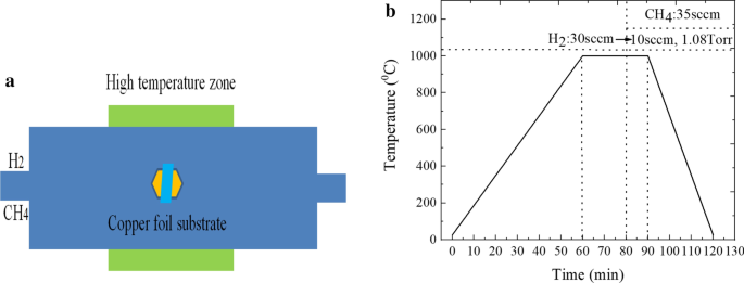
a グラフェン成長と b のCVDシステム図 グラフェン成長中の温度曲線
ご存知のように、多結晶銅箔はグラフェンの品質に影響を与えるため、グラフェンの成長実験の前に銅箔基板をアニールする必要があります。ステージ1でのアニーリングプロセスの具体的な条件は次のとおりです。アニーリング温度、時間、および水素の流量(H 2 )ガスはそれぞれ1000°C、20分、30sccmでした。このとき、銅箔の表面は大面積の単結晶ドメインを形成し、H 2 ガスは酸化銅を還元することができ、それは高純度の銅基板を得ることができます。ステージ2に入る間、成長温度は一定のままです。H 2 の流量 ガスは10sccmに調整され、その間に35 sccmのメタン(CH 4 )ガスも導入され、成長時間と成長圧力はそれぞれ10分と1.08 Torrに維持され、CVD実験ではグラフェンの成長速度は約16μm/ sでした。これにより、比較的均一な単分子層の調製が保証されます。グラフェン膜[27、28]。最後に、管状炉を一定の速度で室温まで急冷しました。これにより、基板の表面の損傷を防ぐことができます。
以下に、単層グラフェン材料のSiO 2 への移動固有のプロセスについて説明します。 / Si基板[29]。まず、質量分率4%のPMMA溶液を、1cm×1cmのサイズの単層グラフェン材料の表面に均一にスピンコーティングしました。回転速度と時間は、それぞれ3000 R / minと1minでした。次に、銅箔基板を(NH 4 ) 2 (SO 4 ) 2 質量分率が3%の溶液で、処理時間は3〜4時間でした。次に、ガラススライドによるPMMA /グラフェンを脱イオン水で2〜3回繰り返しすすぎ、PMMA /グラフェンをSiO 2 によって50°Cの恒温テーブルに移しました。 / Si基板、単層グラフェン材料とSiO 2 の間の水蒸気を除去できます / Si基板、および単層グラフェン材料は、SiO 2 によりよく付着することができます / Si基板。このステップでは、SiO 2 サイズが1×1cm 2 の/ Si基板 アセトン、エタノール、水で15分間超音波洗浄し、SiO 2 の表面を洗浄しました。 / Si基板は非常にクリーンで均一であり、グラフェン/ TMDのヘテロ構造の成長を促進します。最後に、PMMA /グラフェン/ SiO 2 / Siをアセトン溶液に3〜4時間入れて、PMMAを溶解し、アルコールと脱イオン水で繰り返し洗浄して、単層グラフェン膜をSiO 2 に転写できるようにしました。 / Si基板。
グラフェン/ TMDのヘテロ構造の準備
CVDデュアル温度ゾーン管状炉では、グラフェン/ SiO 2 / Si基板はMoS 2 の成長に使用されました およびWS 2 材料。 MoO 3 、WO 3 成長モリブデン源、タングステン源、硫黄源としてそれぞれ硫黄粉末を使用した。高純度Arガスは、グラフェン/ MoS 2 の調製にも使用されました。 およびグラフェン/ WS 2 それぞれヘテロ構造。まず、100mgの硫黄粉末を入れた石英ボートを管状炉の上流に置きました。次に、2 mg MoO 3 粉末(またはWO 3 粉末)を別の石英ボートに充填し、グラフェン/ SiO 2 / Si基板をMoO 3 で上下逆さまにしました 粉末(またはWO 3 粉)。そして、グラフェン/ SiO 2 を搭載したクォーツボート / Si基板とMoO 3 粉末(またはWO 3 粉末)を管状炉の高温領域に挿入しました。図2aに示すように、加熱ベルトを石英管に巻き付けて硫黄粉末を加熱しました。これにより、硫黄粉末が適切に制御され、均一に蒸発するようになります。次に、キャリアガスとして流量50sccmの高純度Arガスを使用し、硫黄粉末の蒸発温度を150℃、MoS 2 の成長温度と成長時間を制御しました。 およびWS 2 それぞれ750°C、920°C、10分でした。その間、第1段階の温度は100°Cで10分間維持され、管状炉の水蒸気を除去することができます。具体的な温度変化図を図2bに示します。その後、硫黄粉末が硫黄蒸気に昇華し始め、硫黄蒸気は管状炉の高温領域に到達し、Arガスによって駆動することができます。 MoO 3 と完全に反応することができます およびWO 3 粉末、および生成物はグラフェン/ SiO 2 に堆積されました / Si基板。したがって、グラフェン/ TMDヘテロ構造の成長速度は、TMD材料の成長速度と一致していました[30]。 MoS 2 の成長後 およびWS 2 材料、管状炉は自然に室温まで冷却され、基板の色は淡黄色になります。
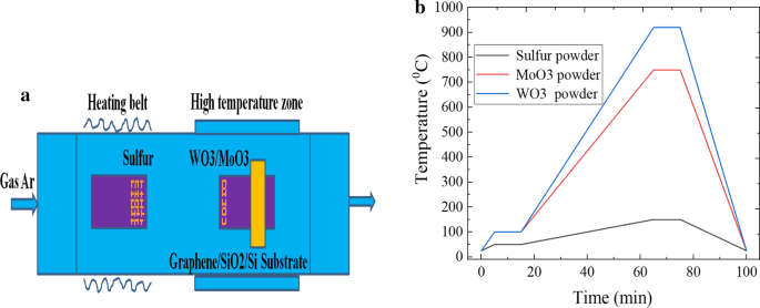
a グラフェン/ TMDのヘテロ構造と b の準備概略図 成長温度と時間の関係曲線
グラフェン/ TMDのヘテロ構造のテスト特性
この論文では、グラフェン/ TMDヘテロ構造の試験および特性評価方法には、主に光学顕微鏡(OM)、ラマンおよび光ルミネセンス(PL)分光法、電界放出型走査電子顕微鏡(FESEM)、エネルギー分散型X線分光法( EDX)および原子力顕微鏡(AFM)。まず、グラフェン/ TMDのヘテロ構造の表面形態を、光学顕微鏡、SEM、およびAFMで観察できます。ヘテロ構造の層数は、ヘテロ構造サンプルのコントラストの違いから判断できます。次に、グラフェン/ TMDヘテロ構造のスペクトル特性をテストし、特性を評価しました。グラフェン表面上のTMD材料の成長形態、成長パターン、および成長メカニズムを分析し、特性評価の結果に基づいて推測しました[31]。次に、ラマン分光法には、2D材料の特性評価に関して、迅速性、高効率、低破壊性という利点があります。サンプル表面での電子フォノンの相互作用を直接観察することができ、2D材料で非常に幅広い用途があります。 2D材料の層数と結晶品質は、ラマンスペクトルの特徴的なピーク位置、グラフェン/ TMDヘテロ構造の特徴的なピーク位置の波数差、およびその他の特性を分析することによって効果的に判断できます。最後に、PLスペクトルは、2D材料の特性評価と分析のための重要な方法でもありました。バルク材料が単層材料に薄くなると、TMD材料のバンドギャップ幅は間接バンドギャップ半導体から直接バンドギャップ半導体に変化します。一方、蛍光効果は大幅に向上し、PLスペクトルには明らかな特徴的なピークがあります。ただし、グラフェン/ TMDヘテロ構造の結晶品質が高くない場合、サンプルの層または単分子層が少ない場合でも、PLスペクトルの特徴的なピーク強度は小さくなります。したがって、サンプルの層厚と結晶品質は、PLスペクトルによっても判断できます。さらに、グラフェン/ TMDヘテロ構造フィルムの分布、元素タイプ、および濃度パーセンテージは、FESEMおよびEDXによって取得できます。一方、AFMテストは、ヘテロ構造フィルムサンプルの表面の清浄度、粗さ、および材料の厚さを把握するためにも使用されました。
PLスペクトルとラマンスペクトルの両方が、HORIBA Jobin Yvon(フランスの会社)によって製造されたLabRAM HREvolution高分解能ラマン分光計によって収集されました[32、33]。ラマンおよびPLスペクトルの範囲は300cm -1 でした –3000 cm -1 それぞれ550〜800nmです。また、ラマンスペクトルとPLスペクトルは、それぞれ10%のパワーと5%のパワーでした。以下は、特定のテスト条件であり、スペクトル分解能≤0.65cm -1 ;空間分解能:水平≤1μm、垂直≤2μm; 532 nmレーザー、50倍の対物レンズ(ビームスポット径は1.25 µm、100%レーザー出力は7500 µw / cm 2 に相当 );スキャン時間は15秒で、累積数は2です。
結果と考察
グラフェン/ WSの光学顕微鏡写真と特性評価 2 ヘテロ構造
ヘテロ構造の形態は、ラマン分光計の高解像度顕微鏡によって区別することができます。図3aは、グラフェン/ WS 2 の光学顕微鏡画像を示しています。 SiO 2 の異なる位置でのヘテロ構造 / Si基板。グラフェン膜の色がSiO 2 に転写されたので / Si基板はそれほど違いはなく、グラフェン膜は比較的均一で完全です。グラフェン/ SiO 2 の表面 / Si基板は、少量の粒子を除いてきれいでした。これは、より高品質のグラフェン膜の存在を示しています。一方、WS 2 の核形成密度 WS 2 の成長実験でガス濃度が十分なときに最大になりました 。そしてWS 2 グラフェン/ SiO 2 で成長 / Si基板は、粒子表面が均一で一辺の長さが約120μmの三角形構造の粒子でした。 WS 2 の形 規則的で完全であり、厚さは均一であり、機械的剥離サンプルのサイズよりもはるかに大きい[34]。図3bでは、WS 2 の蛍光強度が サンプルは非常に均一に分布しており、三角形の単分子層WS 2 フィルムはより高い品質とより低い欠陥を持っています。図3c、dから、WS 2 の形態がわかります。 フィルムサンプルは三角形で、WS 2 の厚さ フィルムは0.83nmであり、単層WS 2 の準備を示しています。 映画。さらに、SEMはWS 2 の形態を分析するためにも使用されました。 サンプルフィルムであり、形態は図3eに示すように、均一な厚さの規則的な三角形でした。図3fでは、ドック元素、硫黄元素、および炭素元素がEDXスペクトルで示されています。これは、グラフェン/ WS 2 ヘテロ構造の材料は正常に転送され、準備されます。
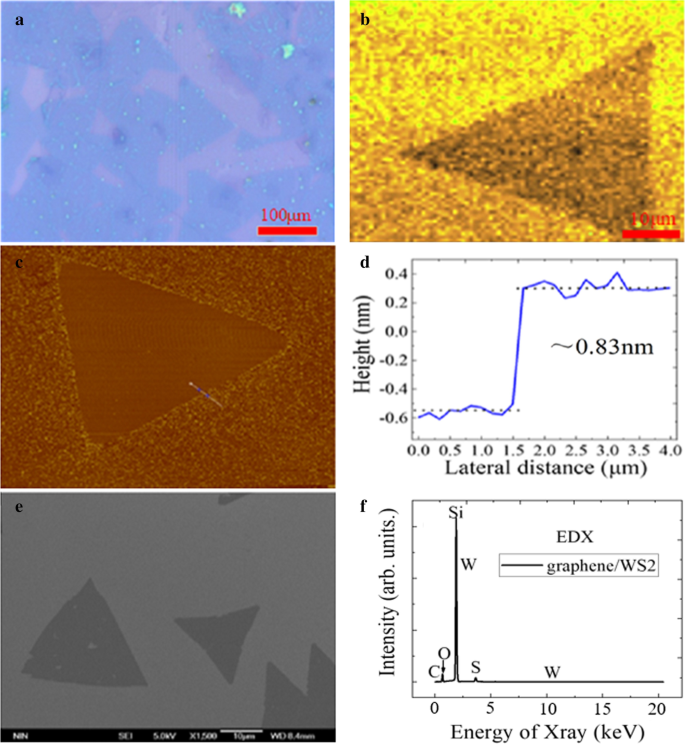
a 光学顕微鏡写真、 b マッピング画像、 c AFM画像、 d 高さプロファイル画像、 e FE-SEM画像と f グラフェン/ WS 2 のEDXスペクトル SiO 2 上のヘテロ構造 / Si基板
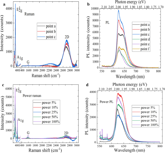
材料の分子振動と回転情報は、材料構造を特定するための指紋振動スペクトルであるラマン分光法によって取得できます。 WS 2 の層数と結晶品質 サンプルは、ラマンスペクトルの特徴的なピーク位置と波数差によって効果的に判断できます。図4aは、WS 2 のラマンスペクトルを示しています。 さまざまな位置でのサンプル、E 1 2g およびA 1g 特徴的なピークは350.4cm -1 にありました および416.1cm -1 、 それぞれ。バルクWS 2 の場合 単層材料への変更、E 1 2g およびA 1g 特徴的なピークは、それぞれ青方偏移と赤方偏移で表示されます。したがって、層数は2つの特徴的なピーク間の波数の差で判断でき、波数の差は65.7 cm -1 でした。 、したがって、三角形のWS 2 粒子は単層材料でした。図4bでは、最も強い発光ピークは626 nmにあり、対応するバンドギャップは1.98 eVでした。これは、単分子層WS 2 のバンドギャップ幅と一致しています。 。ご存知のように、2D材料のPL強度は、結晶品質と層数に関係しています。 2D材料は欠陥と層数が少なく、光度が高いため、結晶品質が優れていることを示しています[35]。可変出力の特性評価は、レーザー照射によるサンプルの損傷を防ぐために、nWレベルで実行できます。図4cを観察すると、E 1 のピーク位置がわかります。 2g 平面振動モードは、励起パワーの増加に伴って基本的に変化せず、A 1g 平面間の振動モードは短波数方向に移動します。これは、A 1g 振動モードは電子濃度と大きな関係があり、電子濃度の増加はバンドギャップの再形成につながります。図4dに示すように、WS 2 のPLスペクトル強度 レーザー出力が増加すると増加し、バンドギャップの再形成とヘテロ構造の層間相互作用に起因する蛍光消光現象が存在します。同時に、材料の局所温度は、レーザー出力の増加に伴ってほとんど変化しなかったことがわかります。これは、WS 2 が原因です。 は原子層レベルのナノ材料です。
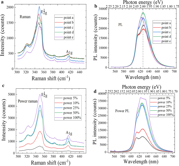
WS 2 のスペクトル特性 。 a さまざまな位置でのラマンスペクトル、 b さまざまな位置でのPLスペクトル、 c パワーラマンスペクトルと d パワーPLスペクトル
グラフェン材料の層数の特性評価と品質情報は、ラマン分光法によって取得できます。図5aでは、さまざまな位置でのグラフェンのラマン回折スペクトルには、Dピーク、Gピーク、2Dピークの3つの主要な特徴的なピークがあり、それぞれ1330 cm -1 にあります。 、1583 cm -1 および2674cm -1 。 Dピークはグラフェンの格子構造の乱れに関係しており、グラフェン材料の格子欠陥が多いほどDピークの位置が青方偏移し、結晶の欠陥や不純物含有量を反映している可能性があります。 2Dピークは、2フォノンの2次共鳴ラマンピークであり、グラフェン材料の炭素原子配列を示すことができます。また、GピークはE 2g によって引き起こされます 最初のブリルアンゾーン中心のモードでは、ピーク高さはグラフェンの層数にほぼ直線的に増加し、Gピーク強度はある程度グラフェンのドーピングに関連しています。 2DピークとGピークの相対比を使用して、グラフェンの層数を大まかに決定できます。欠陥密度が増加すると、DピークとGピークの比は減少します。弱いDピークは、MoS 2 の成長時にグラフェンのラマンスペクトルに現れます。 (またはWS 2 )材料が完成しました。これは、グラフェンドメインが依然として高品質を維持していることを示しています。露出したグラフェン領域の2Dピーク強度が弱まり、これは高温成長プロセスの影響を受けます。グラフェン2Dピークの半値全幅(FWHM)は、層数の増加とともに徐々に増加し、2Dピークのピーク位置は青方偏移します。これは、グラフェン材料のエネルギーバンド関係に関連している可能性があります。電子エネルギーバンド構造は層数の増加とともに分裂し、さまざまなフォノン共鳴散乱過程が発生します。励起子のピークは、より多くのエネルギーを吸収することによって励起され、2Dピーク位置の青方偏移につながります。ポイントCおよびEでのGピークのピーク強度は、2Dピークのピーク強度よりも大幅に高くなっています。 私 2D / 私 G 厚さが増すにつれて比率は減少し、この実験で転写されたグラフェンはあまり均一ではなく、許容範囲内にあります。図5bは、単層グラフェンのパワーラマンスペクトルを示しています。グラフェンのGおよび2Dピーク強度は、レーザー出力と温度の上昇とともに徐々に増加し、基本的にピーク位置とFWHMの変化はありません。 Gピークと2Dピークは、それぞれ1581 cm -1 にありました。 および2672cm -1 、および2つの特徴的なピークの強度は大きく異なります。グラフェンとその下にあるSiO 2 の間の相互作用の変化による 、 I の特徴的なピーク比 2D / 私 G 減少します。一方、ラマンスペクトルのD欠陥ピークはありませんでした。これは、選択したグラフェン領域の品質が高く、炭素原子が高度に秩序化されていることを示しています。
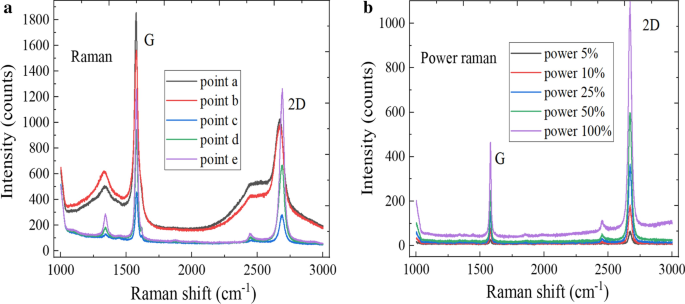
グラフェンのスペクトル特性。 a さまざまな位置と b でのラマンスペクトル パワーラマンスペクトル
ラマン分光法を使用して、グラフェン/ WS 2 の特性評価と分析を行いました。 ヘテロ構造の材料であり、300 cm -1 の2つのスペクトルがありました ≤ω ≤500cm -1 および1400cm -1 ≤ω ≤3000cm -1 、ローレンツ関数によって適合されました。 E 1 がありました 2g およびA 1g WS 2 のモード特性ピーク 300 cm -1 の範囲 ≤ω ≤500cm -1 。 E 1 2g フォノンモードは硫黄原子とタングステン原子の面内変位であり、A 1g フォノンモードは硫黄原子の面外変位であり、上記のフォノンモードの位置と間隔は層の数によって異なります。グラフェンのGおよび2Dピークは、1400 cm -1 のスペクトル領域に表示されます。 ≤ω ≤3000cm -1 、グラフェンの層数と結晶品質の情報は、強度比と特徴的なピークのピーク位置から取得できます。
2つの異なるDavydov分割ピークの周波数差は、vdWsヘテロ構造の相互作用の大きさを反映している可能性があります。したがって、多層2D材料の層内振動フォノンモード周波数は、層間結合と層数にも依存します。図6aは、グラフェン/ WS 2 のラマンスペクトルテストの特性を示しています。 532nmレーザーの下のさまざまなポイントでのヘテロ構造。 E 1 の強度が 2g 特徴的なピークはA 1g よりも高かった 特徴的なピーク強度、およびE 1 2g およびA 1g 特徴的なピークは349.3cm -1 にありました および417.1cm -1 、 それぞれ。グラフェン/ WS 2 のラマンスペクトル2DおよびGピーク ヘテロ構造は、それぞれ1591.5 cm -1 でした。 および2680.9cm -1 、および2DおよびGピークのピーク位置は、純粋なグラフェンと比較して上昇します。これは、WS 2 の効果的な層間結合に関連している可能性があります。 ナノシートとCVD成長中の高温加熱によって生成されるひずみ効果。グラフェン/ WS 2 のラマンスペクトル ヘテロ構造材料は、個別に分離されたWS 2 の合計にすぎません。 グラフェンスペクトル。vdWsヘテロ接合界面の形成を確認できます。 PLスペクトル強度は、結晶品質と層数に関連しています。ラマン分光法は、振動モードに対するヘテロ構造形成の影響に焦点を当てており、TMDヘテロ構造材料の電子バンド構造は主にPLスペクトルによって取得できます。図6bは、グラフェン/ WS 2 のPLスペクトルを示しています。 異なるポイントでのヘテロ構造。最も強い発光ピークは624nmにあり、対応するバンドギャップは1.99 eVでした。これは、単分子層WS 2 のバンドギャップ幅と一致しています。 。グラフェン/ WS 2 異なる位置にあるヘテロ構造材料は、PLスペクトルの強度と形状が異なり、結晶品質はあまり良くありません。したがって、ヘテロ構造の調製プロセスをさらに改善する必要があります。グラフェン/ WS 2 のPLスペクトル強度 ヘテロ構造はWS 2 よりも弱いです 。これは、グラフェン/ WS 2 の層間結合が原因です。 ヘテロ構造は、ヘテロ構造領域の励起子蛍光を変化させます。これにより、電子正孔対の分離と蛍光の減少が起こります。一方、グラフェン/ WS 2 の場合、ピーク位置がシフトします。 ヘテロ構造が形成され、電荷の移動によりフェルミ面がシフトし、自由励起子が荷電励起子に変化する可能性があります。図6cは、グラフェン/ WS 2 のパワーラマンスペクトルを示しています。 ヘテロ構造。面内フォノンモードE 1 2g 特徴的なピークと面外フォノンモードA 1g 特徴的なピークは、それぞれ356 cm -1 でした。 および418cm -1 、ここで、上記の特徴的なピークは、レーザー出力の増加とともに増加します。特徴的なピークのピーク位置と形状は単結晶内で均一であり、WS 2 の電子特性 グラフェン/ SiO 2 / Si基板は均一でした。 WS 2 の厚さ シートは、A 1g 間の周波数差に応じて決定できます。 およびE 1 2g 特徴的なピークであり、平均距離は62±0.2 cm -1 、これは単分子層WS 2 の厚さと一致しています 。固有のグラフェンのピーク位置と比較して、グラフェン/ WS 2 のGピークと2Dピーク位置 1578.7 cm -1 のヘテロ構造 および2685.8cm -1 1582.2 cm -1 に変更します および2689.5cm -1 、 それぞれ。また、Gピークの強度は、レーザー出力の増加に伴い2Dピークの強度よりも強くなり、 I が減少します。 2D / 私 G グラフェンとSiO 2 間の相互作用の変化によって引き起こされる比率 / Si基板[36、37]。図6dを観察すると、グラフェン/ WS 2 のPL強度がわかります。 レーザー出力の増加に伴い、ヘテロ構造が増加します、 PLスペクトルの半値幅も増加し、PLスペクトルの形状が変化します。その理由は、ヘテロ構造周辺の試験温度が上昇し、グラフェン/ WS 2 の界面にも強い層間結合があるためです。 ヘテロ接合。
グラフェン/ WS 2 のスペクトル特性 ヘテロ構造。 a さまざまな位置でのラマンスペクトル。 b さまざまな位置でのPLスペクトル。 c パワーラマンスペクトル;および d パワーPLスペクトル
グラフェン/ WS 2 のラマンスペクトル 図7aに示すように、ヘテロ構造は露出したグラフェン領域の構造とは大幅に異なっていました。まず、波数が増加するとスペクトルのバックグラウンドが上昇し、バックグラウンドはWS 2 のPLスペクトルに由来します。 、グラフェン/ WS 2 の存在を確認します ヘテロ構造。次に、WS 2 材料は、グラフェンの2D特性ピーク強度を抑制することができます。最後に、グラフェン/ WS 2 のGピークと2Dピークの両方 ヘテロ構造は、裸のグラフェン材料のスペクトルと比較して上方にシフトします。グラフェンとWS 2 の間の層間結合による , the 2D peak would also shift up, and the mechanical strain also has the impact on the Raman shift of graphene. The enhancement factor (EF) is the ratio of the maximum peak intensity of graphene/WS2 hetero-structure divided by the maximum peak intensity of graphene. The maximum peak intensity of G peak increases from 460 to 830, and the maximum peak intensity of 2D peak increases from 340 to 1460, and the corresponding EF were 1.8 and 4.3, respectively. The D peak signal is significantly enhanced when the graphene/TMDs hetero-structures is formed. Therefore, the I D / 私 G ratio of monolayer graphene is weaker than that of graphene/WS2 hetero-structure. This is because the extrusion of WS2 on graphene has the effect on the structure of graphene, which would result in the appearance of a small number of defects. In Fig. 7b, the PL intensity of graphene/WS2 hetero-structure is higher than that of bare graphene, which may be related to the effective interlayer coupling and the strain effect. Meanwhile, the maximum intensity of PL spectra is increased from 270 to 1410, and the corresponding EF is 5.23. The intensity enhancement of characteristic peak can be attributed to the coupling of graphene/WS2 hetero-structure.

a ラマンスペクトルと b PL spectra characteristics comparison of graphene before and after WS2 growth
Raman spectroscopy can be used to evaluate the crystal quality and film thickness of 2D materials. The Raman spectra comparison of WS2 and graphene/WS2 hetero-structure is shown in Fig. 8a. Compared to the Raman spectra of WS2 , the A1g mode characteristic peak position of graphene/WS2 hetero-structure was blue-shifted, and the intensity of E 1 2g mode and A1g mode characteristic peaks was higher than those of WS2 , and the graphene/WS2 hetero-structure film has the excellent crystallinity. The reason is that the coupling between layers can be enhanced when the two materials are stacked to form the hetero-structure, which would generate the interlayer interaction forces. The maximum E 1 2g and Alg characteristic peak intensity increases from 3400 and 1100 to 6500 and 2950, respectively. And the enhancement factors (EF) are 1.9 and 2.7, respectively. In addition, monolayer WS2 and multilayer WS2 are the direct band gap semiconductor and indirect semiconductor materials, respectively. Therefore, the PL spectroscopy can be used to identify the layer number of WS2 サンプル。 In Fig. 8b, the above two materials show that the strongest PL emission was around 626 nm, and that the band gap was approximately at 1.98 eV, which is consistent with band gap of the mechanically peeled monolayer WS2 。 The PL intensity of graphene/WS2 hetero-structure was stronger than that of monolayer WS2 。 The reasons are the following:First, the work function between graphene and WS2 does not match. Second, the internal field was formed. Third, the photoelectrons from WS2 can transfer to graphene. Forth, the WS2 material retains holes. The maximum intensity of strongest peak increases from 7450 to 19,320, and the EF of PL spectra are 2.6. The increase in peak intensity is due to the coupling between graphene and WS2 materials.

a ラマンスペクトルと b PL spectra characteristics comparison between WS2 and graphene/WS2 hetero-structure
Optical Micrograph and Characterization of Graphene/MoS2 Hetero-structure
The optical microscope pictures of graphene/MoS2 hetero-structure on SiO2 /Si substrate are shown in Fig. 9a. We found that the color of the graphene transferred to SiO2 /Si substrate was not much different from the original one. The surface was relatively clean except for a few particles in some areas. These results indicate that the graphene film is uniformly and completely formed. MoS 2 thin film covers graphene/SiO2 /Si substrate, which can be connected into the continuous graphene thin film across the grain boundaries. The prepared graphene/MoS2 hetero-structure was continuous and intact, and the sample surface was relatively clean, which has the good surface uniformity. The local fluorescence intensity distribution is not uniform when there are many defects. Figure 9b shows the in-plane fluorescence intensity distribution of triangular monolayer MoS2 映画。 The crystal lattice of sample has the fewer defects. In Fig. 9c, d, the surface condition of the material is observed by AFM, and the height difference between the edge of the material and the graphene/SiO2 /Si substrate is measured to judge the material thickness, the thickness of monolayer MoS2 material is about 0.81 nm. It can be found by the SEM test result that the morphology of MoS2 film sample is the triangular flake, as shown in Fig. 9e. It can be found by observing Fig. 9f that the molybdenum, sulfur and carbon elements are uniformly distributed in the EDX spectrum, which indicates that the graphene/MoS2 hetero-structure has been successfully prepared.

a Optical micrograph, b mapping image, c AFM image, d height profile image, e FE-SEM image and f EDX spectrum of graphene/MoS2 hetero-structure on SiO2 / Si基板
The interlayer interaction weakens with decrease in the film thickness. A 1g mode characteristic peak is red-shifted, whereas the characteristic peak of E 1 2g mode is blue-shifted. As a result, the frequency distance between A1g およびE 1 2g vibration modes becomes smaller, which can be used to identify the thickness of 2D materials. Figure 10a shows the Raman spectra of MoS2 at different positions. The characteristic peaks of E 1 2g mode and A1g mode were at 381.2 cm −1 and 400.5 cm −1 、 それぞれ。 And the peak spacing was 19.3 cm −1 , which indicates the presence of monolayer MoS2 。 Due to the Van der Waals force between the layers, the frequencies of two vibration modes moving in the same or opposite directions between adjacent atoms in the layers are slightly different. The PL spectra are used to obtain the light emission characteristics of MoS2 film, as shown in Fig. 10b. As we all know, the luminous intensity of monolayer MoS2 was much greater than that of multilayer, and the electronic band structure changed from indirect band gap to direct band gap when the layer number of MoS2 material changed from multilayer to single layer. Therefore, there was only the strong emission peak of monolayer MoS2 。 In addition, the strongest PL peak was at 678.5 nm, and the corresponding direct band gap was 1.83 eV, which is close to the band gap value of mechanically peeling MoS2 映画。 It can be found by observing Fig. 10c that the characteristic peak intensity of Raman spectra is increased with increase in the laser power and that the peak positions of E 1 2g およびA 1g mode characteristic peak were blue-shifted. This is because the Raman peak line would have a certain frequency shift with increase in the temperature and laser power. Figure 10d shows the power PL spectra of MoS2 , the luminous intensity increasing accordingly with increase in the laser power, and the strongest PL peak position was blue-shifted.

Spectral characteristics characterization of MoS2 。 a Raman spectra at different positions, b PL spectra at different positions, c power Raman spectra and d power PL spectra
A high-frequency layer vibrating phonon mode of monolayer 2D material would split into the N corresponding high-frequency modes in an N-layer 2D material, which would lead to the Davydov splitting. Figure 11a shows the Raman spectra of graphene/MoS2 hetero-structure, and there were the G, 2D peaks of graphene and the E 1 2g およびA 1g MoS 2 のピーク , which indicates the formation of layered graphene/MoS2 hetero-structure material. E 1 2g およびA 1g Raman characteristic peaks of MoS2 were located at 375.5 cm −1 and 394.4 cm −1 、 それぞれ。 And the peak spacing was 18.9 cm −1 。 Compared with intrinsic graphene, the G peak and 2D peak positions of graphene/MoS2 hetero-structure shift to large wavenumbers, and G peak and 2D peak move from 1581 and 2672 cm −1 to 1587 and 2674 cm −1 、 それぞれ。 In addition, the intensity of G peak is stronger than that of 2D peak. The rise of the 2D and G peaks position is related to the effective interlayer coupling and the strain effect. Compared with the Raman spectra of MoS2 material, the spectra of graphene/MoS2 hetero-structure material are significantly shifted due to the enhancement of interlayer atomic interaction, and the peak intensity can also be significantly enhanced. It can be found from Fig. 11b that the graphene/MoS2 hetero-structure has two absorption peaks at 621 nm and 683 nm and that the corresponding band gaps were 1.99 eV and 1.82 eV according to the conversion relationship between wavelength and electron volt. The luminous intensity of graphene/MoS2 hetero-structure was lower than that of intrinsic MoS2 。 The reasons of these phenomena are that the graphene material has the weakening effect on the fluorescence of MoS2 material and that the electronic energy band and electronic distribution can be changed due to the interlayer coupling, which can greatly change the PL and Raman spectra.

Spectral characteristics of graphene/MoS2 hetero-structure. a Raman spectra at different positions, b PL spectra at different positions, c power Raman spectra and d power PL spectra
Figure 11c shows the power Raman spectra of graphene/MoS2 hetero-structure, the Raman peaks intensity of G, 2D, E 1 2g , and A1g increasing with increase in the laser power. The peak position difference between E 1 2g およびA 1g is gradually enhanced with increase in the layer number of MoS2 材料。 The characteristic peak positions of E 1 2g およびA 1g were 377.2 cm −1 and 396.7 cm −1 、 それぞれ。 And the peak position difference was 19.5 cm −1 , which can be judged that MoS2 material is the monolayer. Meanwhile, the G and 2D peaks of graphene were red-shifted and blue-shifted, respectively. This is because graphene material is doped with MoS2 。 It can be found by observing Fig. 11d that there were two PL peaks of graphene/MoS2 hetero-structure. These PL peak corresponding to the compound transition of A and B excitons, wherein the light emission corresponding to the direct band gap exciton recombination was 1.84 eV, whereas the peak corresponding to the indirect band gap exciton recombination was at 2.0 eV. The luminous intensity of strongest peak is increased with increase in the laser power, and the peak position of the strongest PL spectra is red-shifted. This is due to the p -type conductivity of the graphene and the change of band structure when graphene and MoS2 materials were stacked. In addition, the arrangement of energy bands at the interface allows the electrons from electron-rich MoS2 to transfer to p -type graphene material.
結論
Graphene/TMDs-based hetero-structures, where WS2 およびMoS 2 were used as TMDs material, were successfully synthesized directly on graphene films by using APCVD. The morphology, spectral characteristics and luminescence law of hetero-structures can be obtained by AFM, SEM, EDX, Raman and PL spectroscopy, and the hetero-structures show the excellent photosensitivity. Compared with intrinsic graphene material, the G and 2D peak positions of graphene/TMDs hetero-structures are the blue-shifted, the intensity of G peak is stronger than that of 2D peak with increase in the laser power and decrease in the I 2D / 私 G 比。 Due to the presence of internal electric field, the photo-generated electron–hole pairs can be effectively separated at the interface of graphene/TMDs hetero-structures, which could greatly improve the light response. This research could effectively guide the preparation process improvement in large-area, high-quality hetero-structures, and it could also pave the way for the application of graphene/TMDs hetero-structures in the optoelectronic devices field.
データと資料の可用性
The experiment data supporting the conclusion of this manuscript have been given in this manuscript.
略語
- 2D TMDs:
-
Two-dimensional transition-metal dichalcogenides
- vdWs:
-
ファンデルワールス
- HEMT:
-
High-speed electron mobility transistors
- PMMA:
-
ポリメチルメタクリレート
- MoS 2 :
-
二硫化モリブデン
- APCVD:
-
Atmospheric pressure chemical vapor deposition
- WO3 :
-
Molybdenum trioxide
- OM:
-
光学顕微鏡
- PL:
-
フォトルミネッセンス
- MoO3 :
-
Molybdenum trioxide
ナノマテリアル
- ハードウェア、材料、ソフトウェア:3Dプリントの成功の3つの柱
- 3D印刷材料市場の進化:2019年の傾向と機会
- SLSの進化:新技術、材料、アプリケーション
- 社内の研究開発
- BPは大学と連携して、工学材料と腐食を研究しています
- スピーカーとイヤホンのグラフェン
- ICAをロードしたmPEG-ICAナノ粒子の調製とLPS誘発性H9c2細胞損傷の治療におけるそれらの応用
- スタックカップカーボンナノファイバーの原子および電子構造を明らかにする
- チタン酸塩ナノチューブで装飾された酸化グラフェンナノコンポジット:調製、難燃性、および光分解
- Li-Nb-O化合物の調製と光触媒性能に及ぼすLi / Nb比の影響
- 航空宇宙部品および精密航空機部品市場