


抵抗変化型メモリ(RRAM):材料、スイッチングメカニズム、パフォーマンス、マルチレベルセル(mlc)ストレージ、モデリング、およびアプリケーションの概要
要約
この原稿では、抵抗変化型メモリ(RRAM)技術の分野における最近の進歩は、その高速性、低コスト、拡張されたストレージ密度、さまざまな分野での潜在的なアプリケーション、および優れた機能により、最も傑出した新興メモリ技術の1つと見なされています。スケーラビリティが包括的に見直されます。最初に、新しいメモリ技術の分野の概要を説明します。 RRAMの材料特性、抵抗スイッチングメカニズム、および電気的特性について説明します。また、耐久性、保持、均一性、動作温度とランダム電信ノイズ(RTN)の影響などのさまざまな問題が詳しく説明されています。ストレージ密度の向上と低コストを実現するために魅力的なRRAMのマルチレベルセル(MLC)ストレージ機能について説明します。信頼性の高いMLC操作を実現するためのさまざまな操作スキームとその物理的メカニズムが提供されています。さらに、さまざまな一般的なRRAMモデルのスイッチング方法と電流電圧の関係について詳しく説明します。セキュリティ、ニューロモルフィックコンピューティング、不揮発性ロジックシステムなどのさまざまな分野へのRRAMの将来のアプリケーションについて簡単に説明します。現在の総説は、RRAMの課題と将来の展望に関する議論で締めくくられています。
はじめに
RAMと呼ばれるランダムアクセスメモリは、揮発性または不揮発性のいずれかです。揮発性メモリは、ダイナミックランダムアクセスメモリ(DRAM)およびスタティックランダムアクセスメモリ(SRAM)の場合と同様に、電源を取り外すと以前に保存されたデータを失います。不揮発性メモリの場合、以前に保存された内容は、電源を取り外した後も保持され続けます。フラッシュメモリは、不揮発性メモリの典型的な例です。メモリテクノロジーは、長所と短所を組み合わせて、より高いパフォーマンスを実現します。コンピュータシステムで採用されているDRAMは容量と密度が高いですが、揮発性であるため、数ミリ秒ごとに更新する必要があります。このリフレッシュにより、デバイスのエネルギー消費量が増加しますが、これは望ましくありません。一方、SRAMは高速ですが、DRAMと同じように揮発性もあります。さらに、SRAMセルはサイズが大きいため、大規模な実装が妨げられます。フラッシュメモリは、基本的に各メモリセルのフローティングゲートに加えて金属酸化膜半導体電界効果トランジスタ(MOSFET)で構成されており、低コストで高密度であるため、現在、特に組み込みアプリケーションで広く使用されています。 。メモリーセルの構成に応じて、フラッシュメモリはNORフラッシュとNANDフラッシュに分類されます[1]。 NORフラッシュでは、セルはビットラインに並列に接続されているため、個別に読み取られてプログラムされます。これは、CMOSNORゲートアーキテクチャのトランジスタの並列接続に似ています。 NANDフラッシュの場合、セルがビットラインに直列に接続されているため、アーキテクチャはCMOSNANDゲートのアーキテクチャに似ています。並列接続に比べて直列接続で消費されるスペースが少ないため、NANDフラッシュのコストが削減されることに注意する必要があります。ただし、どちらのタイプのフラッシュメモリにも、動作速度の低下(書き込み/消去時間:1 ms / 0.1 ms)、耐久性の制限(10 6 )などのいくつかの欠点があります。 書き込み/消去サイクル)、および高い書き込み電圧(> 10 V)[2]。
上記のメモリ技術、つまりDRAM、SRAM、およびフラッシュは、電荷ストレージベースのメモリです。 DRAMはコンデンサに電荷の形で情報を保存し、SRAMは交差結合インバータのノードに電荷を保存することに基づいていますが、フラッシュメモリ技術はトランジスタのフローティングゲートを使用して電荷を保存します。これらの既存の電荷ストレージベースのメモリテクノロジーはすべて、現在、10nmノード以上にスケールダウンするという課題に直面しています。これは、ナノスケールで蓄積された電荷が失われ、その結果、パフォーマンス、信頼性、およびノイズマージンが低下することに起因します。さらに、DRAMの大容量リフレッシュダイナミックパワーとSRAMとDRAMの両方のリークパワーの要件は、将来のメモリ階層の設計に深刻な課題をもたらします。
そのため、通常は新興メモリ技術と呼ばれる新しいクラスのメモリが現在開発中であり、既存のメモリ階層に革命を起こすことを目的として、主に業界で活発に研究されています[3]。これらの新しいメモリテクノロジーは、SRAMのスイッチング速度、DRAMに匹敵するストレージ密度、およびフラッシュメモリの非揮発性を統合することを目的としているため、将来のメモリ階層にとって非常に魅力的な代替手段になります。
メモリデバイスを理想的なデバイスとして分類するには、次の特性が必要です。低い動作電圧(<1 V)、長いサイクル耐久性(> 10 17 サイクル)、強化されたデータ保持時間(> 10年)、低エネルギー消費(fJ /ビット)、および優れたスケーラビリティ(<10 nm)[4]。ただし、これらの理想的な特性を満たす単一のメモリはこれまでありません。これらの理想的なメモリ特性の一部を満たすために、さまざまな新しいメモリテクノロジが積極的に調査されています。情報を保存するために電荷ではなく抵抗の変化に依存するこれらのメモリ技術は次のとおりです:(i)相変化メモリ(PCM)、(ii)スピン伝達トルク磁気抵抗ランダムアクセスメモリ(STT-MRAM)、および( iii)抵抗変化型メモリ(RRAM)。相変化メモリでは、スイッチング媒体はカルコゲニド材料(通常はGe 2 )で構成されます。 -Sb 2 -Te 5 、GST)[5–7]。 PCMは、効率的なデータストレージ機能を実現するために、結晶相とアモルファス相の抵抗の違いに依存しています。結晶相はデバイスの低抵抗状態(LRS)またはオン状態を示し、アモルファス相は高抵抗状態(HRS)またはオフ状態を示します。 SET操作は一般に論理値「1」を格納することを指すLRSに対応し、RESET操作はデバイスに論理値「0」を格納するHRSに対応します。 SET動作の場合、PCMは電圧パルスの印加時に結晶化温度を超えて加熱されますが、RESET動作の場合、より大きな電流がセルを通過し、その後突然遮断されて溶融し、材料を急冷して、アモルファス状態を実現します。
スピン伝達トルク磁気抵抗ランダムアクセスメモリでは、ストレージ機能は、2つの強磁性層とそれらの間に挟まれたトンネリング誘電体で構成される磁気トンネリングジャンクション(MJT)[8–10]によるものです。参照層の磁気方向は固定されていますが、外部電磁場の印加により、自由強磁性層の磁気方向が変わる可能性があります。参照層と自由層の磁化方向が同じである場合、MTJはLRSにあると見なされます。 MTJの場合、HRSに入ると、2つの強磁性層の磁化の方向は逆平行になります。 RRAMは、2つの金属(M)電極の間に挟まれた絶縁層(I)で構成されています[11、12]。 RRAMは、2つの電極間の絶縁体におけるLRSとHRSにそれぞれ対応する導電性フィラメントの形成と破壊に依存しています[13–15]。
既存のメモリテクノロジと新しいメモリテクノロジの詳細な比較を表1に示します。表から明らかなように、STT-MRAMとPCMには、SRAMに比べて面積が小さいという利点があります。 STT-MRAMは、高速の書き込み/読み取り速度、長い耐久性、および低いプログラミング電圧を提供しますが、PCMには、書き込みの待ち時間が長いという欠点があります。 RRAMは、フラッシュに比べてプログラミング電圧が低く、書き込み/読み取り速度が速いため、フラッシュメモリの潜在的な代替品と見なされています。新たに登場したすべてのメモリテクノロジ候補の中で、RRAMには、製造の容易さ、単純な金属-絶縁体-金属(MIM)構造、優れたスケーラビリティ、ナノ秒の速度、長いデータ保持、現在のCMOSテクノロジとの互換性など、大きな利点があります。将来のデジタルメモリのソリューション[16]。 RRAMの最も重要な利点を図1に示します。
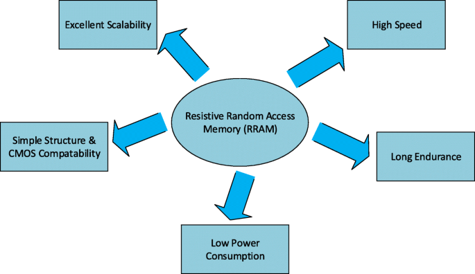
RRAMの利点
この作業では、最近の進歩とRRAMテクノロジの詳細な概要を示します。スイッチング材料のレビューとスイッチングモードの分類およびスイッチングメカニズムの詳細については、「抵抗変化型メモリ(RRAM)」のセクションで説明します。 「抵抗変化型メモリ(RRAM)のパフォーマンスメトリクス」セクションでは、RRAMのさまざまなパフォーマンスメトリクスに焦点を当てています。 RRAMのマルチレベルセル(MLC)特性と、さまざまなMLC操作スキームおよびそれらの物理メカニズムは、「マルチレベル抵抗変化型メモリ(RRAM)」セクションで分析されます。 RRAMデバイスのモデリングの詳細については、「RRAMデバイスのモデリング」セクションを参照してください。 「RRAMのアプリケーション」セクションでは、RRAMのさまざまなアプリケーションについて説明します。最後に、RRAMの課題と将来の見通しを「課題と将来の見通し」セクションに示します。このレビュー原稿の作成で参照された論文のカテゴリーごとの分布を図2に示します。
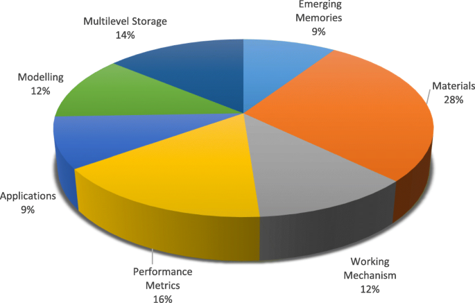
RRAMのレビューの準備のために相談された論文のカテゴリーごとの配布
抵抗変化型メモリ(RRAM)
抵抗スイッチング材料
一部の絶縁体では、印加された電界の印加下で抵抗の変化が発生することが観察されています。抵抗の変化のこの特性は、将来の不揮発性メモリを開発するために最近調査されました[17]。抵抗スイッチング現象はさまざまな酸化物で観察されていますが、主にCMOS BEOL処理との互換性があるため、二元金属酸化物が将来の不揮発性メモリアプリケーションの好ましいスイッチング材料として広く研究されています。酸化ハフニウム(HfO x )などの不揮発性抵抗スイッチングを示すさまざまな金属酸化物ベースの材料 )[18–23]、酸化チタン(TiO x )[24–31]、酸化タンタル(TaO x )[32–36]、酸化ニッケル(NiO)[37–40]、酸化亜鉛(ZnO)[41–46]、チタン酸亜鉛(Zn 2 TiO 4 )[47]、酸化マンガン(MnO x )[48、49]、酸化マグネシウム(MgO)[50]、酸化アルミニウム(AlO x )[51–53]、および二酸化ジルコニウム(ZrO 2 )[54–58]が最も注目を集めており、過去数年間に広く研究されてきました。これらの金属酸化物は、通常、パルスレーザー堆積(PLD)、原子層堆積(ALD)、および反応性スパッタリングによって堆積されます。ただし、ALDは、薄膜の厚さと均一性を正確に制御できるため、広く推奨されている方法です[59]。
従来の電子デバイスでは、電極材料がキャリアの輸送経路として機能するため、電極材料の選択が重要です。 RRAMの場合、電極材料の選択はデバイスのスイッチング動作に大きく影響します。たとえば、銅/ポリ(3-ヘキシルチオフェン):[6,6]-フェニル-C61-酪酸メチルエステル/インジウムスズ酸化物(Cu / P3HT:PCBM / ITO)構造では、安定した抵抗スイッチング動作が観察されました。;しかし、Cu電極をPt電極に交換すると消失しました[60]。 RRAMの電極としては多種多様な材料が利用されています。電極材料は、単体電極、シリコンベースの電極、合金電極、酸化物電極、亜硝酸塩ベースの電極など、その組成に基づいて5つのカテゴリに分類できます。最も豊富で一般的に使用される電極は、Al [51]、Ti [49]、Cu [30]、グラフェン[61]、カーボンナノチューブ[62]、Ag [41]、W [36]、およびPt [44]。シリコンベースの電極の場合、使用される電極のタイプはp型Siとn型Si [63]のみです。合金電極は通常、抵抗スイッチング動作を安定させ、主にCu-Ti [64]、Cu-Te [65]、およびPt-Al [66]を含みます。最も一般的な窒化物ベースの電極は、TiNとTaNです[67、68]。酸化物ベースの電極は、AlドープZnO [69]、GaドープZnO [70]、ITO [71]など比較的豊富です。
RRAMデバイスの製造に最近使用された金属酸化物材料のリストと、上部電極と下部電極に使用される材料のさまざまな組み合わせを表2に示します。さまざまなパラメータの詳細な比較も示しています。使用されている多種多様な材料から、さまざまな種類の酸化物で不揮発性抵抗スイッチングが広く観察されていることが予測できます。 RRAMを製造するための材料の選択は、半導体技術で現在使用されている酸化物を利用することで金属酸化物金属(MOM)構造を簡単に製造できるため、RRAMに優位性をもたらします。 RRAMの下部電極材料は通常プラチナであり、エッチングが少し難しいです。単一デバイス構造の場合、RRAMは同じ下部電極を共有できますが、クロスバーアーキテクチャの場合、デバイスごとに個別の下部電極が使用されます。それらは、物理蒸着とリフトオフを連続して行うことで得られます。上部電極と抵抗スイッチング層は、原子層堆積(ALD)または物理蒸着(PVD)のいずれかを使用して堆積されます。
<図>抵抗切り替えモード
抵抗変化型メモリ(RRAM)は、一般にMIM構造と呼ばれる金属-絶縁体-金属構造を持つ抵抗スイッチングメモリセルで構成されます。この構造は、2つの金属(M)電極の間に挟まれた絶縁層(I)で構成されています。 RRAMセルの概略図と断面図をそれぞれ図3aとbに示します。
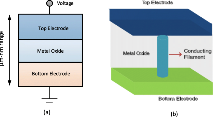
a RRAMの金属-絶縁体-金属構造の概略図。 b RRAMの断面図
RRAMセルに外部電圧パルスを印加すると、デバイスを高抵抗状態(HRS)、または一般に論理値「0」と呼ばれるオフ状態から低抵抗状態(LRS)、または一般にオン状態に遷移させることができます。論理値「1」と呼ばれ、その逆も同様です。抵抗スイッチング(RS)現象は、RRAMセルの抵抗値のこの変化の背後にある理由であると考えられています。準備されたままのRRAMは最初は高抵抗状態(HRS)にあり、デバイスをHRSからLRSに切り替えるために、高電圧パルスの印加によりスイッチング層に導電性パスを形成し、RRAMセルを切り替えます。 LRSに[72]。金属絶縁体金属(MIM)構造のソフトブレークダウンによって発生するこのプロセスは、通常「電鋳」と呼ばれ、このプロセスが発生する電圧は形成電圧( V )と呼ばれます。 f )。形成電圧はセル面積[73]と酸化物の厚さ[74]に依存することがわかっていることに注意する必要があります。ここで、RRAMセルをLRSからHRSに切り替えるために、RESET電圧( V )と呼ばれる電圧パルスを使用します。 リセット )が適用され、この切り替え遷移が可能になります。このプロセスは「RESET」プロセスと呼ばれます[75–78]。 RRAMのHRSは、電圧パルスの印加時にLRSに変更できます。 HRSからLRSへの遷移が発生する電圧は、SET電圧( V )と呼ばれます。 set )、このプロセスは「SET」プロセスと呼ばれます[79]。 RRAMセルからデータを効率的に読み取るために、セルの現在の状態を乱さない小さな読み取り電圧を印加して、セルが論理0(HRS)状態か論理1(LRS)状態かを判断します。 LRSとHRSはどちらも、印加電圧を取り除いた後もそれぞれの値を保持するため、RRAMは不揮発性メモリです。印加電圧の極性に応じて、RRAMは(i)ユニポーラスイッチングと(ii)バイポーラスイッチングの2種類のスイッチングモードに分類できます[80]。ユニポーラスイッチングでは、さまざまな抵抗状態間のデバイスのスイッチング(セットおよびリセットプロセス)は、印加電圧の極性に依存しません。つまり、図に示すように、同じ極性で大きさが異なる電圧を印加するとスイッチングが発生する可能性があります。 4a。一方、バイポーラスイッチングでは、さまざまな抵抗状態間のデバイスのスイッチング(セットおよびリセットプロセス)は、印加電圧の極性に依存します。つまり、HRSからLRSへの遷移は、1つの極性(正または負)および反対の極性は、図4bに示すように、RRAMセルをHRSに戻します。ユニポーラスイッチングでは、ジュール熱は、リセット操作中に導電性フィラメントを破壊する原因となる物理的メカニズムとして解釈されます。一方、バイポーラスイッチングでは、ジュール熱が依然として移動の加速に寄与しますが、荷電種の移動が導電性フィラメント溶解の主な推進力です。確実にするために、コンプライアンス電流( I )であるRRAMの形成/硬化プロセス中に誘電体スイッチング層が恒久的に破壊されることはありません。 cc )はRRAMデバイスに適用されます。コンプライアンス電流( I cc )は通常、セル選択デバイス(トランジスタ、ダイオード、抵抗)によって、またはオフチップテスト中に半導体パラメータアナライザによって保証されます。
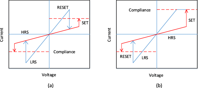
RRAMのI-V曲線。 a ユニポーラスイッチングと b バイポーラスイッチング[4]
抵抗スイッチングメカニズム
RRAMセルの切り替えは、誘電体内の導電性フィラメント(CF)の成長に基づいています。 CFは、メモリセルの上部電極と下部電極を接続するナノメートルオーダーの非常に小さい直径を持つチャネルです。フィラメントを接続すると低抵抗状態(LRS)が得られ、電極間にギャップを空けてフィラメントを切断すると高抵抗(HRS)が得られます[91]。導電性フィラメントの組成に基づいて、RRAMは次の2つのタイプに分類できます。(i)導電性ブリッジランダムアクセスメモリ(CBRAM)とも呼ばれる金属イオンベースのRRAMと(ii)フィラメントベースのRRAMと呼ばれる酸素空孔'OxRRAM'として。ここで、CBRAMは電気化学的金属化メモリ(ECM)と呼ばれることもありますが、「OxRRAM」は原子価変化メモリ(VCM)と呼ばれることもあることに注意してください。
「CBRAM」とも呼ばれる金属イオンベースのRRAMでは、抵抗変化の原因となる物理的メカニズムは、金属イオンの移動とそれに続く還元/酸化(レドックス)反応に基づいています[92、93]。 CBRAM構造は、Ag、Cu、Niなどの酸化可能な上部電極(アノード)、比較的不活性な下部電極(カソード)、たとえばW、Pt、および2つの電極間に挟まれた金属酸化物層。このようなメモリセルでのフィラメント形成は、活性金属電極(最も一般的にはAgまたはCu)の溶解、陽イオン(Cu + )の輸送によって発生します。 またはAg + )、およびその後の不活性下部電極での堆積または還元[94]。したがって、このタイプのRRAMの抵抗変化型動作は、金属フィラメントの形成と溶解によって支配されます。
金属イオンベースのCBRAMのスイッチングメカニズムをよりよく理解するために、Ag / a-ZnO / PtRRAMセルの例を考えてみましょう[41]。導電性ブリッジランダムアクセスメモリセルのスイッチングプロセスを示す一般的な概略図を図5に示します。CBRAMメモリセルの元の状態を図5aに示します。 Ag上部電極(TE)はフィラメント形成の活性成分であり、下部Pt電極は不活性です。 Ag上部電極に正の電圧バイアスを印加すると、酸化(Ag→Ag + + e − )上部電極で発生するため、Ag + 陽イオンが生成され、Ag電極から誘電体層(a-ZnO)に堆積します。 Pt下部電極(BE)の負のバイアスは、Ag + を引き付けます 陽イオン、およびそのようなものとして、還元反応(Ag + + e − →Ag)は下部電極で発生します。したがって、Ag + 陽イオンはAg原子に還元され、導電性ブリッジが形成されるまで蓄積し(図5b–d)、RRAMデバイスはLRSを示すと言われています。このプロセスは「SET」と呼ばれます。印加電圧の極性を逆にすると、導電性の高いフィラメントがほぼ完全に溶解し、デバイスは高抵抗状態(HRS)になっていると言われます。このプロセスは「リセット」と呼ばれ、図5eに示されています。
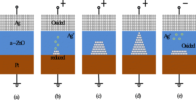
導電性ブリッジRRAMのスイッチングメカニズムの概略図。 a RRAMデバイスの元の状態。 b 、 c Agの酸化とAgの移動 + 陰極への陽イオンとその還元。 d Ag原子とPt電極の蓄積は、高導電性フィラメントの成長につながります。 e フィラメントの溶解は、反対の極性の電圧を印加すると起こります[41]
酸素空孔ベースのRRAM(OxRRAM)では、抵抗変化に関与する物理的メカニズムは、一般に酸素空孔( V )の生成に関連しています。 \(_ {o} ^ {2 +} \))およびその後の酸素イオンの再配置(O 2- )、したがって、RRAMセルの上部電極と下部電極の間に導電性フィラメントの形成を可能にします[59]。最初に、製造されたままのRRAMセルの場合、成形プロセス、つまり誘電体のソフトブレークダウンが不可欠です。ソフト絶縁破壊が発生すると、アノード界面に向けて高電界を印加すると、酸素原子が格子からノックアウトされ、酸素イオンになります(O 2- )一方、酸素空孔( V \(_ {o} ^ {2 +} \))は酸化物層に残ります。酸素イオン(O 2- )貴金属が界面酸化物層を形成するためのアノードの材料として使用される場合、アノード材料と反応するか、中性の非格子酸素として放出されます。したがって、電極/酸化物界面は「酸素貯蔵庫」のように動作します[85]。次に、酸素空孔の蓄積( V バルク酸化物の\(_ {o} ^ {2 +} \))は、導電性フィラメント(CF)が形成され、かなりの電流がデバイスに流れると、RRAMセルを低抵抗状態(LRS)に切り替えます。デバイスを高抵抗状態(HRS)に戻すために、リセットプロセスが発生し、その間に酸素イオン(O 2- )アノード界面からバルク酸化物に戻り、酸素空孔( V )と結合します。 \(_ {o} ^ {2 +} \))または、金属CF沈殿物を酸化してフィラメントを部分的に破壊し、それによってRRAMセルをHRSに戻します。ユニポーラスイッチングメカニズムを示すRRAMセルの場合、酸素イオンの拡散(O 2- )はジュール熱電流によって熱的に活性化されるため、濃度勾配により、酸素イオンが界面またはCF周辺の領域から拡散します。また、CF周辺の局所温度を上げるためにユニポーラスイッチングRRAMでは比較的高いリセット電流が必要であることに注意する必要があります。一方、バイポーラスイッチングRRAMでは、酸素イオン(O 2- )界面層が重要な拡散障壁を示す可能性があり、純粋な熱拡散では不十分であるため、逆電界によって支援される必要があります。どちらの場合もCFの部分的な破裂が発生し、RRAMセルが高抵抗状態(HRS)に切り替わることに注意する必要があります。これは主に、酸素空孔( V )の形成によるものです。 \(_ {o} ^ {2 +} \))と貧弱な領域により、電子のトンネリングギャップが生じます。デバイスをLRSに戻すために(SETプロセス)、ギャップ領域でのソフトブレークダウンの結果としてCFが電極を再接続します。同様のセット/リセットプロセスは、何サイクルも繰り返すことができます。
上記の議論に基づいて、電気化学的金属化メモリ(ECM)としても知られるCBRAMは、Ag、Cu、またはNiなどの電気化学的活性金属電極に依存して金属カチオンベースのCFを形成します[95]。原子価変化メモリ(VCM)としても知られる酸素空孔フィラメントベースのRRAM「OxRRAM」のCFは、貯蔵材料自体の内部での陰イオンの移動による、金属原子ではなく酸素空孔欠陥で構成されます[96]。 「OxRRAM」と「CBRAM」の両方のスイッチングメカニズムについて詳しく説明しますが、両方のRRAMタイプのスイッチングメカニズムについてはまだ議論があります[97]。たとえば、CFがセットプロセスで成長し始める場所、リセットプロセスで中断する場所、およびこれらの酸素空孔/金属原子がどのように集まってCFを形成するかなどです。 Ta / TaO x の20回の連続スイッチングサイクルの電流-電圧(I-V)特性 / Pt [98]ベースのRRAM構造が調査され、連続するスイッチングサイクルでLRSとHRSの両方の明確な変動が観察されました。その結果、全体的なメモリウィンドウが減少し、全体的なRRAMパフォーマンスが低下します。このサイクルごとの抵抗の変動は、主にCFのランダムな形成と、それぞれセットおよびリセット操作中の破裂に起因します。
さまざまな操作パラメーターに基づくOxRRAMとCBRAMの比較を表3に示します[81、84、86–88、99、100]。この比較により、これらのRRAMメモリタイプの耐久性特性の点で顕著な違いが明らかになります。この相違点は、CBRAMの導電性フィラメントが主に金属原子で構成されており、酸素空孔に比べてドリフトや拡散が比較的容易であるため、OxRRAMに比べてCBRAMの保持時間と耐久特性が低下するためです。両方のRRAMタイプのスイッチングメカニズムは異なりますが、2つの間に多くの共通の特徴があります。唯一の重要な違いは、OxRRAMの耐久性がCBRAMよりも大幅に高いことです。
<図>抵抗変化型メモリ(RRAM)のパフォーマンスメトリック
耐久性
抵抗変化型メモリには、高抵抗状態(HRS)と低抵抗状態(LRS)の間の頻繁な遷移が含まれます。抵抗状態間の各スイッチングイベントは、永続的な損傷を引き起こし、RRAMのパフォーマンスを低下させる可能性があります。したがって、耐久性は、RRAMデバイスをHRSとLRSの間で確実に区別できる比率を確保しながら、それらの間で切り替えることができる回数として定義されます[101]。したがって、耐久性テストでは、HRSとLRSを区別できなくなる前に効果的に切り替えることができるセット/リセットサイクルの最大数を決定します。 RRAMの耐久性特性は、抵抗変化型スイッチングセルで一連のI-V掃引を実行し、続いて R を抽出することによって得られます。 HRS および R LRS 読み取り電圧(通常0.1 V)の印加について[41]。この方法は、各サイクルでデバイスの正しいスイッチングを取得できるため、信頼性があります。ただし、特に低電流が含まれる場合、I-V掃引を取得するために必要な時間が非常に長くなる可能性があるため、この方法は非常に低速です。
H の耐久サイクル f O x 図6aに示すように、RRAMセルはセルサイズに強く依存します。ここでは、セルサイズが大きいRRAMデバイスでの耐久性が向上していることが報告されています。さらに、層の厚さを垂直に薄くすると、図6bに示すように2.5VでのSET電圧の耐久性能が低下します[102]。スイッチング層のダウンスケーリングに伴う耐久性能のこの低下は、アクティブ領域のイオン数の減少の結果です。 H f O x ベースのRRAMは、10 6 の優れた耐久性能を示します 0.18 μ未満の30nmセルサイズの1kbアレイでのサイクル mテクノロジーと同じものを図6cに示します[103]。 A のレイヤーを追加する l O x 下部電極(BE)の上では、HRSの読み取り妨害耐性が向上するため、アレイの安定性をさらに向上させることができます。 T の場合 a O x ベースのRRAMでは、パルス幅とRESET電圧の振幅の増加に伴う耐久性能の低下がTa / Ta 2 で観察されました。 O 5 / TiNRRAM構造[105]。 Ta / Ta 2 のTiNとRu下部電極の比較 O 5 / TiN RRAMは、耐久性の低下の主な原因が、酸素イオンとTiN電極との反応によるものであることを示しています。さらに、10 9 の耐久性が向上しました スイッチングサイクルは、Ta 2 を減らすことにより、同様のRRAM構造で検証なしで取得されました。 O 5 3 nmまでの層[106]で、幅が5ns未満の三角パルスを使用します。大規模アレイのパフォーマンスについては、2 Mb Ta 2 の比較 O 5 10 5 前後のメモリ 耐久性試験のサイクルを図6dに示します[104]。セル電流分布は、初期サイクルと最終サイクルでわずかな変動を示しています。また、LRSのセル電流は50 μを下回ります A、アレイの低消費電力を示します。耐久性が10 12 を超える抵抗スイッチングデバイス cycles have been reported in different types of RRAM cells involving tantalum oxide (TaO x )-based switching mediums [32, 36, 59]. Thus, tantalum oxide-based RRAM devices seem to be exhibiting the highest endurance.

a Endurance cycles of H f O x -based RRAM at different SET voltage and cell size b with different thickness (T5=2 nm, T20=10 nm) at 2.5 V set voltage. c Resistance distribution of 1-kb array obtained from Weibull plots under different endurance cycles. d 100 k cycles endurance of 2-Mb-Ta2 O 5 -based array; Reprinted from refs [102–104]
Retention
The data retention of a RRAM device involves investigating stability over a period of time for both LRS and HRS after undergoing set and reset transitions. In other words, the time period for which a memory cell will remain in a particular state after the set/reset operation determines the capability of a memory cell to retain its content [11]. The application of the constant voltage stress (CVS) over time using a low read voltage (0.1 V) and the measurement of the current versus time (I-t) curve for both LRS as well as the HRS enables the measurement of state retention. Due to the dispersing nature of atomic rearrangements induced in RRAM because of set voltage, the long retention time in LRS is difficult to obtain whereas, in HRS, retention is not a concern as it is usually the natural state of the device and RRAM will continue to remain in this state if no bias (or low bias) is applied. The retention in the LRS depends on the compliance limit during the SET transition, e.g. in RRAMs based on conductive filament switching mechanism, the larger compliance current produces a stronger conducting filament which is more stable over time [28, 41], as compared to a smaller compliance current. A projected endurance of 10 years at 85 ∘ C has been demonstrated in Ti/HfO2 /TiN [18]. A commonly used method to obtain device endurance is by applying read pulse at high temperature after certain time intervals (e.g. every 1 s) and extrapolate the resistance to a 10-year period. Although this method is easy to implement, it has certain limitations primarily due to the read voltage stress applied to the cell. An alternative method is to change the temperature and record the time until the device fails. Activation energy is extracted by plotting the Arrhenius plot and extrapolate down to the operating temperature. However, the limitation of this method is that waiting is necessary until the failure occurs in the RRAM cell, and thus, this method is more time-consuming and expensive.
The device characteristics of H f O x -based RRAM [81, 103] developed at the Industrial Technology Research Institute, Taiwan, are demonstrated to further understand the working of RRAM device. The transmission electron microscopy (TEM) image of the TiN/Ti/ H f O x /TiN RRAM device with 30-nm cell size is shown in Fig. 7a. The device exhibits bipolar switching characteristics and the I-V curve obtained at 200 μ A set compliance current is shown in Fig. 7b. The device presents endurance of 10 6 switching cycles with the resistance on/off ratio greater than 100 at set/reset programming conditions of + 1.5 V/– 1.4 V pulse with 500 μ s pulse width and the same is depicted in Fig. 7c.

a Transmission electron microscopy (TEM) image of TiN/Ti/HfO x /TiN RRAM device. b Typical current-voltage (I-V) characteristics of the device with 30-nm cell size. c 10 6 endurance switching cycles obtained from 500 μ s pulse. d A retention lifetime of 10 years is expected by testing at 150 ∘ C; reprinted from refs. [81, 103]
Uniformity
In RRAM cell, poor uniformity of various device characteristics is one of the significant factors limiting the manufacturing on a wider scale. The switching voltages, as well as both the HRS and the LRS resistances, are among the parameters exhibiting a high degree of variation. The variations of the resistance switching include temporal fluctuations (cycle-to-cycle) and spatial fluctuations (device-to-device). The stochastic nature of the formation and rupture of conductive filament is believed to be the main reason for these variations. Cycle-to-cycle and device-to-device variability is a major hindrance for information storage in RRAM devices [59]. The observation of cycle-to-cycle variability is influenced by the change in the number of oxygen vacancy defects that arise in the CF due to its stochastic nature of formation and rupture during the switching event [107]. Due to this random nature of the CF, the prediction and the precise control of the shape of the CF becomes extremely challenging. This variability becomes worse as the compliance limit (i.e. compliance current ‘I cc ’) is reduced. On the other hand, for the higher value of ‘I cc ’, the ratio of standard deviation (σ ) and average resistance (μ ) is low, resulting in a smaller LRS resistance spread. This is attributed to the higher defects in the CF, thus forming a well-defined path for current conduction.
RRAM also exhibits device-to-device (cell-to-cell) non-uniformity which also degrades the memory performance by reducing the memory margin between two states. The origin of this variability is attributed to the non-uniformities in the fabrication process such as the thickness of the switching film, etching damages and surface roughness of the electrodes. A lot of research has been conducted to improve the uniformity of RRAM and several methods have been explored for the same. One of the methods utilizes the concept of inserting nano-crystal seeds which confine the paths of the conductive filament by enhancing the effect of local electric field [82, 90, 108]. In Ti/TiO 2−x /Au-based RRAM [28], the induction of platinum (Pt) nano-crystals within the thin TiO 2−x results in an enhanced uniformity of the RRAM cell. The Pt nano-crystals limit the switching effect into regions with high oxygen vacancy generation probability which results in improved uniformity. In another approach, engineering the electrode/oxide interface by embedding appropriate buffer layers is very useful in achieving uniform RRAM operation. In HfO x -based RRAM [109], a thin Al buffer layer is inserted between the TiN electrode and HfO x oxide layer. This results in significant improvement of set voltage distribution as well as the resistance distribution, thus enhancing the uniformity of the device. The improvement in the SET voltage and the resistance distribution of the RRAM device after inserting a thin Al buffer layer between TiN electrode and HfO x bulk oxide and the same is depicted in Fig. 8 [59]. Al atoms are assumed to diffuse into HfO2 thin films, and they tend to localize oxygen vacancies due to the reduced oxygen vacancy formation energy, thus stabilizing the generation of conductive filaments, which helps to improve the resistance switching uniformity.

Uniformity improvement of Al buffered HfO x RRAM compared to HfO x -based RRAM array. a Statistical distribution of SET voltage (V set ) obtained from 100 DC sweep cycles. b HRS and LRS statistical distribution for 100 pulse sweep cycles; reprinted from ref. [59]
In addition to the materials engineering approach, a novel programming method has also been suggested to reduce fluctuations. A multistep forming technique was implemented in W/HfO2 /Zr/TiN [22]-based RRAM to minimize the overshoot current due to the parasitic effects. A multi-step forming technique results in the gradual formation of the filament; thus, a low set/reset current is achieved improving the switching characteristics of the device. Various other methods such as constant voltage forming and hot forming (usually referred to as forming at a higher temperature) have also been investigated to effectively reduce the resistance variations [110]. Another method of achieving high uniformity is by applying a pulse train rather than a single pulse to a RRAM cell [23]. This approach not only results in improved uniformity but also enhances the multilevel capability of a RRAM cell.
Effect of Operating Temperature and Random Telegraph Noise
To achieve a reliable performance of the RRAM device, the effect of operating temperature and random telegraph noise (RTN) is investigated. It is observed that the resistance of both the LRS and HRS states undergoes variations because of the change of operating temperature. The temperature study of TiN/HfO2 /Ti/TiN [111] was carried out. A positive sweep voltage of <3 V magnitude and compliance current of 1 μ A was applied for the electroforming. Once forming takes place, a reset voltage (V リセット ) <–1 V switches the device back to the HRS (OFF state). To switch the device back to the LRS (ON state), set voltage (V set ) <1 V is applied.
The reset operation in RRAM device tends to show voltage-controlled negative differential resistance (NDR). The reset operation occurs abruptly at low temperatures, while for temperatures above room temperature, the reset process takes place more gradually. The resistance of the RRAM device in the pristine state, as well as the ON state and OFF state as a function of temperature is depicted in Fig. 9a. The semiconducting behavior is observed for the pristine state as well as the OFF state, i.e. resistance decreases with increase of temperature. For the ON state, a metallic characteristic is observed, i.e. resistance increases with increase of temperature. Due to the variation of resistance with change in temperature, R OFF /R ON also decreases from a value of 20 to approximately 5 over the temperature range of 213–413K. In Ti/HfO x /Pt devices, decrease in R OFF /R ON was observed with temperature-dependent cycling. This decrease in resistance ratio was attributed to the built-up of oxygen-vacancy-related traps inside the HfO2 metal oxide layer [112, 113]. Additionally, temperature-dependent measurements without set/reset operation were carried out to evaluate the impact of I-V cycling on the R OFF /R ON 比。 The sweep voltage across the RRAM device was stopped before reaching V set および V リセット 値。 For OFF state resistance (green rectangles), a weaker temperature dependence was observed in contrast to the ON state resistance (green circles) which exhibited similar characteristics, compared to the cycling case. From these observations, we infer that I-V cycling induces stronger temperature dependence, which decreases the R オフ / R オン 比。 The effect of temperature variation on the switching voltages V set および V リセット is depicted in Fig. 9b. The slight variation in V set with changing temperature indicates that there is no significant temperature difference. For the case of V リセット , the general trend is that a decrease in voltage value of about 0.2 V with temperature increase in the range of 233–333K is observed. Also, a slow increase of V リセット is observed for 353–413K temperature range.

The effect of varying temperature on a virgin resistance (left axis) and the OFF-state as well as the ON-state resistances (right axis) at 213–413K temperature range and b switching voltages V set および V リセット; reprinted from ref. [111]
Random telegraph noise (RTN) is another factor that affects the performance of RRAM. RTN has for long been used as an indicator of device performance and reliability. RTN decreases the memory margin between the HRS and LRS because of the extensive fluctuations in the read current during the read operation. Due to the effect of RTN, the read margin, scaling potential and the multilevel cell capability of a RRAM cell are greatly affected [114]; thus, it needs to be investigated to achieve reliable performance. To investigate the effect of bottom electrode on RTN, an analysis of Ta2 O 5 / TiO 2 RRAM [115] was carried out. The examples of complex RTN signals in LRS and HRS are depicted in Fig. 10. RTN causes read instability in the RRAM device, thus reducing the read margin, multibit storage implementation and hindering device scaling. The RTN is attributed to the trapping and de-trapping of electrons in the proximity of the CF in LRS whereas it occurs in the tunneling gap in the HRS state. Although the physics of RTN is still not clear and is being highly debated, the electron trapping and de-trapping which temporarily inhibits the charge transport is widely accepted as the mechanism responsible for fluctuation due to RTN. It is observed that with the decrease in operation current, the amplitude of RTN increases, thus highly affecting the HRS level. Therefore, it is necessary to ensure the additional resistance margin to achieve reliable performance. RTN in RRAM has been researched extensively, although the physical mechanism of RTN is still not explicitly defined. RTN can be utilized as a tool to map the movements of active vacancies in RRAM due to its time-dependent variation. This might be quite useful to understand the failure mechanisms of other reliability issues.

Complex RTN signals in LRS and HRS of Ta2 O 5 / TiO 2 -based RRAM depicting normalized noise amplitude and average current; reprinted from ref. [114]
Multilevel Resistive Random Access Memory (RRAM)
Multilevel Per Cell (mlc) Storage
Owing to their small physical size and low power consumption, RRAM devices are potential for future memory and logic applications. Increased storage density is among the most critical aspects of memory technology to enable the design of multibit capacity [89] memory cells. The multiple resistive states can be achieved in RRAM cells which provide benefits of low-cost and high-density non-volatile data storage solutions. Currently, a lot of research is being conducted in the area of RRAM to scale down the dimensions and increase the structural density of memory arrays. Previously, the storage density of RRAM has been increased by the reduction of device size; however, the complexity involved in the experimental procedures limits its successful implementation. Another suggested method is employing three-dimensional (3D) crossbar architectures. Two types of architectures of ‘vertical’ and ‘crossbar RRAM’ have been proposed [116, 117]; however, both these architecture types require advanced fabrication procedures which is not desirable. A much simpler alternative to increase storage density in RRAM devices is by making use of multilevel cell (MLC) storage technology which enables storing more than one bit per cell without reducing the physical device dimensions. This MLC is one of the most promising properties of RRAM which can significantly increase the memory storage density [83, 118–125]. Thus, instead of a single high and low resistance state (HRS and LRS), we can achieve multiple HRS and LRS, without changing the device dimensions. However, to achieve reliable MLC operation, the precise control over the resistance of the different resistance levels of RRAM should be ensured; otherwise, the device will suffer from resistance variability and reliability issues mainly due to the random nature of the conductive filament formation during the switching process [126].
Methods to Obtain Multilevel Per Cell (mlc) Modes in RRAM
The MLC behavior in RRAM makes it very useful for high-density applications. To obtain MLC behavior in RRAM, the following three methods are employed:(i) changing compliance current, (ii) controlling reset voltage and (iii) varying pulse width of program/erase operation.
MLC by Changing Compliance Current
The RRAM device is usually operated with 1-RRAM (1R) cell configuration [41] or in 1-Transistor 1-RRAM (1T-1R) cell configuration [18]. The MLC characteristics in 1R configuration can be obtained by changing the current compliance (I cc ) during ‘set’ operation whereas the MLC characteristics in 1-Transistor 1-RRAM (1T-1R) cell structure are controlled by varying the voltage at the gate of the transistor, which enables the control of compliance current (I cc ) during the set operation of a RRAM cell. The typical MLC I-V curves of Ti/Ta2 O 5 /Pt [127] based RRAM cell are shown in Fig. 11. As the compliance current (I cc ) is increased from 150 μ A to 1 mA, six different LRS are obtained at I cc =150 μ A, I cc =200 μ A, I cc =300 μ A, I cc =500 μ A and I cc =700 μ A, I cc =1 mA due to the increase in the respective current of LRS (I LRS ) while the HRS is maintained constant and the HRS current (I HRS ) remains same for all the LRS levels. For Ti/Ta2 O 5 /Pt RRAM, with the increase in I cc , the maximum reset current (I reset ) also increases while the set voltage is almost maintained constant. Also, it was observed that the resistance of the LRS (R LRS ) decreases while the (I reset ) increases owing to the stronger filament formation with the increase in I cc 。

Multilevel characteristics of Ti/Ta2 O 5 /Pt RRAM obtained by controlling the compliance current. ‘Reproduced from [127], with the permission of AIP Publishing’
The formation of the CF and its corresponding widening with an increase in I cc is the attributed mechanism of multilevel per cell (MLC) in compliance current (I cc ) mode as depicted schematically in Fig. 12. With an increase in the size of CF because of an increase of I cc , the resistance of the CF decreases and hence results in multiple LRS levels for different values of I cc 。 It is also observed that I reset increases with increasing I cc as higher power is required to rupture the CF having larger diameter.

Schematic illustration of multiple resistance states in RRAM cell obtained by varying compliance current ‘I cc ’ [98]
MLC by Controlling Reset Voltage
The MLC characteristics in a RRAM cell can also be obtained by controlling the reset voltage (V リセット ) while (I cc ) is maintained constant. In this case, the typical MLC I-V curves of TiN/HfO x /AlO x /Pt-based RRAM cell [128] by applying different (V リセット ) of − 2.1 V, − 2.7 V and − 3.3 V are shown in Fig. 13.

Multilevel characteristics of TiN/HfO x /AlO x /Pt RRAM obtained by controlling the reset voltage. ‘Reproduced from [128], with the permission of AIP Publishing’
It is observed that with an increase in (V リセット ), the HRS current (I HRS ) decreases; thus, multiple HRS levels with the same LRS resistance are obtained. In addition, the set voltage (V set ) also increases as V リセット is increased while as the I リセット remains almost constant.
The decrease in I HRS with the increase in reset voltage is primarily due to the increase in the gap between the metal electrode and tip of the CF as depicted in Fig. 14. The more the magnitude of the V リセット , the larger the gap and thus the higher the value of resistance. Therefore, an increase in the gap between the CF tip and bottom electrode (BE) with increasing reset voltage results in multiple resistance levels of HRS. It is observed that the devices in which the I リセット shows a gradual change in current instead of the abrupt change during the ‘reset’ operation, the change in HRS resistance in such devices can be due to decrease in the size of the conductive filament (CF) as V リセット is increased. This approach is more viable practically for cross-point architectures as it requires relatively lower complex circuitry.

Schematic illustration of multiple resistance states in RRAM cell obtained by varying reset voltage ‘V reset ’ [98]
MLC by Varying Program/erase Pulse Width
MLC characteristics can also be obtained by varying the program/erase pulse width while the amplitude of the pulse is maintained constant [23]. In HfO x -based RRAM [128], three HRS levels were demonstrated by varying the width of the reset pulse from 50 ns to 5 μ s。 This method of obtaining MLC characteristics in RRAM is relatively easier; however, this scheme is energy inefficient. This drawback limits the application of this method to obtain reliable characteristics in the RRAM cell. The higher energy consumption of the RRAM device was confirmed on the comparison of the transient responses between the reset pulse amplitude and pulse width control. This is particularly due to the higher unwanted energy dissipation as the thermal energy in the resistive switching material.
A summary of RRAM devices exhibiting multiple resistance states is shown in Table 4. As is evident from the table, various RRAM devices with multiple resistance states have been reported. Till date, however, only 8 resistance states have been demonstrated in a single RRAM cell either by varying I cc or V リセット 。 Therefore, there is a huge scope for increasing the number of resistance states in the RRAM cell, thus enhancing its storage density.
<図>Modeling of RRAM Devices
Modeling plays a very critical role in development of devices utilizing semiconductor technologies. To fully understand device operation and to optimize the performance, an accurate model is of great importance. A number of RRAM models with varying features and accuracy have been proposed [129]. This section discusses the characteristics and attributes of the various commonly used RRAM models popular.
Stanford/ASU Model
One of the most popular physics-based RRAM models is the Stanford/ASU RRAM model [130–132], proposed by Guan et al. and Chen et al. This model was applied to validate the I-V switching characteristics of HfO2 RRAM [128] and includes the effect of Joule heating and temperature change on the switching of RRAM devices.
This model is dependent on the CF growth inside a dielectric switching layer. The filament gap, i.e. the gap between the tip of the CF and top electrode, is the internal state variable for this model. The growth of CF inside a dielectric is attributed to the oxygen ion movement and regeneration and recombination of oxygen vacancies [133]. Thus, the rate of change of filament gap (g) is given as [130]:
$$ {\frac{dg}{dt}} =V_{\tiny{0}}.\exp\bigg({{\frac{-E_{a},m}{k_{b}.T}} }\bigg). {\text{Sinh}} \bigg({\frac{qa_{h}\gamma V}{L.k_{b}.T}}\bigg) $$ (1)ここで E a is the activation energy, V is the magnitude of the voltage applied across the device, L is the switching material thickness, a h is the hopping distance, γ is the local field enhancement factor, V 0 is the velocity containing attempt to escape frequency, K b is the Boltzmann constant, q is the elementary unit charge and T is the temperature of the conductive filament.
The spatial variation in the gap size is accounted for in this model, in addition to the variations which arise due to the stochastic property of the ion process. A noise signal is added to the gap distance to account for these variations as [130]:
$$ g_{|t+\Delta t} =F \Big[ g_{|t}, {\frac{dg}{dt}} \Big] + \delta_{g}\times\tilde{X}(n)\Delta t, n ={\frac{t}{T_{GN}}} $$ (2)ここで、Δ t is the simulation time step, the function F represents time evolution of gap size fromt to Δ t。 \(\tilde {X}\)(n) is a zero mean Gaussian noise sequence. T GN is the time interval after which \(\tilde {X}\)(n ) changes to next random value.
The variation in the gap size δ g depends on kinetic energy of ions and filament temperature as [130]:
$$ \delta_{g} (T) ={\frac{\delta^{\tiny{0}}_{g}}{\bigg\{ 1+\exp \Big({\frac{T_{\text{crit}}- T}{T_{\text{smith}}}} \Big) \bigg\}}} $$ (3)where \(\delta ^{0}_{g}\) and T smith are fitting coefficients to match the resistance distribution curves to experiments and T クリティカル is a threshold temperature above which the gap size changes significantly.
This model shows strong dependence on temperature; thus, there is a need to account for the change of ‘T’ 。 With change in cell characteristics, the dynamic inner domain temperature T changes significantly, while the outer domain assumed to be at uniform and stable temperature (T bath ), is related as [130]:
$$ c_{p} {\frac{dT}{dt}} =V(t).I(t) - k(T-T_{\text{bath}}) $$ (4)where C p is the effective heat capacitance of inner domain, V (t) I (t) represents the Joule heating and k is the effective thermal conductivity.
Using a generalized conduction mechanism, the current conduction is defined as [130]:
$$ I(g,v) =I_{\tiny{0}}.\exp\bigg({{\frac{-g}{g_{\tiny{0}}}} }\bigg){\text{Sinh}} \bigg({\frac{V}{V_{\tiny{0}}}}\bigg) $$ (5)ここで私 0 、 g 0 および V 0 are the fitting parameters to match experimental results.
One of the significant features of this model is its implementation in neuromorphic applications and RRAM synaptic device design [134], giving the model a great degree of flexibility and further scope for implementation in various neuromorphic systems.
Physical Electro-thermal Model
Physical electro-thermal model was developed by Kim et al. [135] and implemented with tantalum pentoxide (Ta2 O 5 ) -based bilayer RRAM [136–138]. This physical model solves the differential equations based on finite element solving method. This model also makes use of electrothermal physics phenomenon approach for modeling [139], thus giving it advantage in terms of flexibility to incorporate finite element method (FEM) solver to simulate the system very accurately. However, the drawback of this approach is its difficulty in implementation for SPICE and Verilog circuit solvers.
This model describes CF as a doped region having oxygen vacancies as dopants with CF extending from the top to the bottom electrode of the device. To describe the drift-diffusion of vacancy migration, this model assumes the same equation can be used to describe both the processes of oxygen ions and vacancies. The ion model by Mott and Gurney [140] is employed here to describe the process given as [135]:
$$ {\frac{dn_{D}}{dt}} =\Delta \times \bigg(D_{s}.\Delta_{n\tiny{D}}- \mu v n_{D} \bigg) + G $$ (6)ここで D s describes the diffusion process, v gives the drift velocity of vacancies and G is the CF growth rate which actually describes the SET process. The parameters are defined as [135]:
$$ D_{s} ={\frac{1}{2}} \times a^{2} \times f_{e} \times \exp \bigg({\frac{- E_{a}}{k_{B}T}} \bigg) $$ (7) $$ v =a_{h} \times f \times \exp \bigg({\frac{- E_{a}}{k_{B}T}} \bigg) \times {\text{Sinh}} \bigg({\frac{q a_{h}E}{k_{B}T}} \bigg) $$ (8) $$ G =A \times \exp \bigg({\frac{- (E_{a}-ql_{m}E)}{k_{B}T}} \bigg) $$ (9)where l m is the mesh size.
These equations govern the physical transformation of the device during SET and RESET transition, thus essentially controlling the CF growth and rupture.
Huang’s Physical Model
Huang’s physical model developed by Huang et al. [141, 142] is a very comprehensive physical model for RRAM device as it takes into account both the CF width and the gap of filament to electrode as the factors affecting the state variable dynamics. In addition, temperature distribution is also accounted for in this model.
SET/RESET process is considered as a result of generation/recombination process of oxygen ions (O 2- ) and oxygen vacancies (V 0 )。 During the SET process, CF starts to evolve from the tip of the top electrode (T.E) and elongates in radius with increase in voltage, resulting in final width ‘W’ of the C.F. This model assumes symmetrical cylindrical shape of the C.F. During RESET process, CF ruptures starting from TE till it dissolves completely with increase in voltage. The filament gap distance ‘x’ is defined as the gap between active electrode layer (T.E) and the tip of the C.F.
Thus, for the SET process, parameter ‘W’ acts as state variable, while for RESET, parameter ‘x’ acts as state variable. Therefore, \(\frac {dx}{dt}\) and \(\frac {dw}{dt}\) define the dynamics of the device during the SET/RESET transition.
During the first reset process, CF reduction rate, i.e. release of O 2- , is by the electrode is expressed as [142]:
$$ {\frac{dx}{dt}} =a \times f\times \exp \bigg({\frac{- E_{i}-\gamma Z_{e}V}{k_{B}T}} \bigg) $$ (10)For O 2- hopping within the oxide layer, the CF reduction rate with ‘a’ being the distance between two V0 is given as [142]:
$$ {\frac{dx}{dt}} =a \times f\times \exp \bigg({\frac{- E_{h}}{k_{B}T}} \bigg) {\text{Sinh}} \bigg({\frac{ a_{h}Z_{e}E}{k_{B}T}} \bigg) $$ (11)For the case of RESET process when dominated by recombination between O 2- and V0 is expressed as [142]:
$$ {\frac{dx}{dt}} =a \times f\times \exp \bigg({\frac{- \Delta E_{r}}{k_{B}T}} \bigg) $$ (12)In the initial step of the SET process dominated by recombination of oxygen vacancies with thin CF initially grown is given by [142]:
$$ {\frac{dx}{dt}} =-a \times f_{e}\times \exp \bigg({\frac{- E_{a}-\alpha_{a} Z_{e}E}{k_{B}T}} \bigg) $$ (13)Here, Z およびα g are the fitting parameters.
For the second step, CF grows along its radial direction and is defined as [142]:
$$ {\frac{dw}{dt}} =\bigg(\Delta w + {\frac{\Delta w^{2}}{2w}} \bigg) \times f_{e}\times \exp \bigg({\frac{- E_{a}-\gamma Z_{e}v}{k_{B}T}} \bigg) $$ (14)The current flowing through the device is modeled as a correlation of hopping current with voltage and gap distance expressed by [134] as:
$$ i =i_{0}. \exp \bigg({\frac{-x}{x_{T}}} \bigg) {\text{Sinh}} \bigg({\frac{v}{v_{T}}} \bigg) $$ (15)This model is validated in HfO x /TiO x system [141, 142], and a pretty accurate match between the experimental and simulation results is obtained. Although this model accounts for the significant processes which affect the RRAM operation, however, it has some limitations. The most critical one is being incompatible with the SPICE and Verilog-A.
Filament Dissolution Model
This model was developed exclusively for unipolar RRAM devices by Russo et al. [143–145], however was later modified for bipolar RRAM devices [139, 146] also. Filament dissolution model is based on rupture of CF under the effect of significant temperature change caused due to Joule heating.
One of the significant advantages of this model is that it utilizes the simple partial differential equations to account for the device current and temperature changes due to Joule heating as well as the dissolution velocity. The conduction of current within the device is described by Poisson’s equation [144] as:
$$ \triangledown \times \bigg({\frac{1}{\varphi}\triangledown_{v}} \bigg) =0 $$ (16)Here, φ is the oxide resistivity and v defines the electric potential due to the application of external bias voltage to one of the electrodes while the other electrode is connected to ground.
The CF is divided into a number of mesh grids and at each point of the mesh grid the temperature is calculated to describe the rupture of CF. The Fourier steady-state heat equation describes this effect as [144]:
$$ -\triangledown \times \bigg(k \triangledown T \bigg) =\varphi J^{2} $$ (17)ここで k represents the oxide layer thermal conductivity, J is the current density and T is the device temperature.
The temperature ‘T’ of the device increases to the critical temperature, after which the device is reset and the CF dissolution takes place. The dissolution factor is modeled as [144]:
$$ V_{\text{DIS}} =V_{\text{DIS}-F}. \exp \bigg({\frac{- E_{a}}{k_{B}T}} \bigg) $$ (18)ここで E a is the activation energy, k b はボルツマン定数、 V DIS−F is a fitting parameter and V DIS is velocity of CF boundary towards symmetry axis.
The resistivity of CF is temperature-dependent and is described as [144]:
$$ \varphi_{\text{CF}} (T) =\varphi_{\mathrm{CF-RT}} \Big[ 1 + C (T-T_{0}) \Big] $$ (19)ここで C is the experimentally calculated temperature coefficient of resistivity and φ C F − R T is the standard CF resistivity at room temperature.
COMSOL Multiphysics Software [147] is used for solving the coupled equations for this RRAM model due to its multiphysics capabities and ability to handle such simulations.
Bocquet Bipolar Model
Bocquet bipolar model [148] describes the bipolar oxide-based resistive switching memories utilizing a physics-based modeling approach. Bocquet bipolar model describes the electroforming process of RRAM device, inaddition to utilizing some of the characteristics from Bocquet unipolar model [149] and modifies them significantly according to the bipolar switching characteristics. In this model, the radius of the CF is the internal state variable which effectively governs the switching rate.
To model the electroforming stage, Bocquet bipolar model utilizes electroforming rate (τ Form ) which details the mechanism of conversion to switchable sub-oxide from pristine oxide. The electroforming stage is modeled as [148]:
$$ \tau_{\text{form}} =\tau_{\text{form}0} \times \exp \bigg({\frac{E_{a\text{Form}}-q \times \alpha_{s} \times V_{\text{cell}}}{k_{B}\times T}} \bigg) $$ (20) $$ {\frac{dr_{\text{CFmax}}}{dx}} ={\frac{r_{\text{work}}-r_{\text{CFmax}}}{\tau_{\text{form}}}} $$ (21)ここで E a Form is the activation energy for electroforming, τ form0 is the nominal forming rate, α s is the charge transfer coefficient, V cell is the voltage applied between the top and bottom electrodes, r CF is the radius of CF which varies from 0 to r CFmax 、 q is the elementary charge of electron, T is the temperature of the device and k B is the Boltzmann constant.
The electrochemical redox reaction derived from Butler-Volmer equation [150] is used to describe the SET/RESET operation as [148]:
$$ \tau_{\text{Red}} =\tau_{\text{Redox}} \times \exp \bigg({\frac{E_{a}-q \times \alpha_{s} \times V_{\text{cell}}}{k_{B} \times T}} \bigg) $$ (22) $$ \tau_{Ox} =\tau_{\text{Redox}} \times \exp \bigg({\frac{E_{a}+q \times (1 - \alpha_{s}) \times V_{\text{cell}}}{k_{B} \times T}} \bigg) $$ (23)ここで、τ Red およびτ Ox are the reduction and oxidation rates, respectively. τ Redox is the effective reaction rate considering both reduction and oxidation reactions.
The switching rate is obtained by coupling the above two equations as [148]:
$$ {\frac{dr_{CF}}{dt}} ={\frac{r_{\text{CFmax}}-r_{\text{CF}}}{\tau_{\text{red}}}} - {\frac{r_{\text{CF}}}{\tau_{\text{Ox}}}} $$ (24)Bocquet bipolar model is a quite comprehensive model as it includes the temperature effects as well. The local filament temperature is coupled using heat equation and is given in Eq.(25), the temperature considering a cylindrical-shaped filament is given in Eq. (26). The maximum temperature reached into CF at x =0, the middle of the filament is given in Eq. (27) and the equivalent electrical conductivity in the work area (σ eq ) is given in Eq. (28).
$$ \sigma_{x} \times F(x)^{2} =- k_{th}.{\frac{d^{2}T(x)}{dx^{2}}} $$ (25) $$ T(x) =T_{\text{amb}}+{\frac{V^{2}_{\text{cell}}}{2. L^{2}_{x}.k_{th}}} \bigg({\frac{L^{2}_{x}}{4}- x^{2}} \bigg) \sigma_{eq} $$ (26) $$ T =T_{\text{amb}}+{\frac{V^{2}_{\text{cell}}}{8. k_{th}}} \sigma_{eq} $$ (27) $$ \sigma_{eq} =\sigma_{CF}.{\frac{r^{2}_{\text{CF}}}{r^{2}_{\text{work}}}} - \sigma_{Ox}. {\frac{r^{2}_{\text{CFmax}}-r^{2}_{\text{CF}}}{r^{2}_{\text{work}}}} $$ (28)where (σ x ) is the local electrical conductivity, F ( x ) is the local electric field, σ CF is the electrical conductivity of the conductive filament, k th is the thermal conductivity and T amb is the ambient temperature.
It must be mentioned here that temperature increases with increase in radius of the CF, resulting in self-accelerated reaction due to a positive feedback loop. The self-limited reaction also referred to as SOFT reset [151], on the other hand, occurs due to the decrease in temperature and radius of the CF during RESET operation.
The total current flowing in OxRRAM is the sum of currents flowing in the conductive area (I CF ), the conduction through switchable sub-oxide (I sub−oxide ) and conduction through unswitched pristine oxide (I pristine )。 The total current is as [148]:
$$ I_{\text{cell}} =I_{\mathrm{sub-oxide}} + I_{\text{CF}} + I_{\text{Pristine}} $$ (29) $$ I_{\text{CF}} =F.\pi. \sigma_{CF}.r^{2}_{CF} $$ (30) $$ I_{\mathrm{sub-oxide}} =F.\pi. \sigma_{Ox}. \big(r^{2}_{\text{CFmax}}- r^{2}_{CF}\big) $$ (31) $$ I_{\text{Pristine}} =S_{cell}.A.F^{2}. \exp {\frac{-B}{F}} $$ (32) $$ A ={\frac{m_{e}.q^{3} }{8\pi.h.m^{ox}_{e}.\phi_{b} }} $$ (33)The parameter B e is the metal-oxide barrier height (ϕ b )-dependent and is given as [148]:
$$ if \phi_{b}\geq qL_{x}F:B_{e} ={\frac{8 \pi \sqrt{2m^{ox}_{e} }}{3\times h\times q}} \Big[ \phi^{{\frac{3}{2}}}_{b}- (\phi_{b}-qL_{x}E)^{{\frac{3}{2}}} \Big] $$ $$ \text{otherwise}, B_{e} ={\frac{8 \pi \sqrt{2m^{ox}_{e} }}{3\times h\times q}} \times \phi^{{\frac{3}{2}}}_{b} $$ (34)where m e and \(m^{ox}_{e}\) are the effective electron masses into the cathode and oxide respectively, F =\(\frac {V_{\text {cell}} }{L_{x}}\) is the electric field across the active layer, h is the Planck constant and S cell is the section of the RRAM cell.
Discrete solutions are required to implement the model in an electrical simulator. This model accounts well in that aspect, making it suitable for simulation involving electrical circuits. This model implements equations in Eldo circuit simulator [152]. The discrete solutions are given as [148]:
$$ r_{\text{CFmax}_{i+1}} =\big(r_{\text{CFmax}_{i}}- r_{\text{work}} \big) \times e^{ {\frac{-\Delta t}{{\tau}_{\text{form}}}} } + r_{\text{work}} $$ (35) $$ r_{CF_{i+1}} =\bigg(r_{CF_{i}}- r_{\text{CFmax}_{i}} \times {\frac{\tau_{eq}}{\tau_{\text{Red}}}} \bigg) \times e^{ {\frac{-\Delta t}{{\tau}_{eq}}} } + r_{\text{CFmax}_{i}} \times {\frac{\tau_{eq}}{\tau_{\text{Red}}}} $$ (36) $$ \text{where} { \tau_{eq}} =\frac{\tau_{\text{Red}}\times \tau_{\text{Ox}} }{\tau_{\text{Red}}+\tau_{\text{Ox}}} $$ (37)This model has been verified against electrical characterization from an HfO2 -based system [153]. An important feature of this model is that it can account effectively for device to device variability [154, 155]. One of the major limitations of this model is the lack of current or voltage threshold.
This section presents in detail various characteristics and features of the RRAM models. A comparative analysis of the RRAM models discussed in this work is presented in Table 5.
<図>Applications of RRAM
RRAM is seen as one of the standout candidates among the emerging memory technologies that has the potential for reforming the memory hierarchy primarily due to its high speed, the capability of non-volatile data storage, enhanced storage density and logic computing function. The various novel applications of RRAM are discussed in this section.
>Non-volatile Logic
The instruction codes and the data are transferred by making use of buses between various units in a computer system having von Neumann architecture because of the separate computing and memory unit. This data transferring process results increased energy consumption and time delay, which is commonly referred to as ‘von Neumann bottleneck’. For reducing the impact of von Neumann bottleneck [156], the computing process which utilizes RRAM crossbar array is suggested which alters the memory and computing operations in the same core. In addition, to obtain high integration density and low cost [157], two-terminal compact device structure of RRAM and its 4F 2 array architecture are highly beneficial. For example, to obtain simple Boolean logic functions such as ‘logic NOT’, ‘logic AND’, and ‘logic OR’, we require multiple transistors and each single transistor takes 8−10F 2 範囲。 These logic functions can be realized by making use of two or three RRAM cells, resulting in total approximate area of around 10F 2 only [158].
Till date, several methods have been suggested for realizing Boolean logic functions [159, 160]. Boolean computing is significantly more established compared to existing non-Boolean computing paradigms such as neuromorphic computing and quantum computing. Therefore, energy and cost-efficiency of CPU or MCU can be enhanced without the need to develop new algorithms or software, although there is still a lack of technical solution on how to implement complex computing tasks in a crossbar array. Thus, most of research to date focusses on only basic logic level demonstration as it becomes quite complex to implement a whole computing unit using RRAM array.
Neuromorphic Computing
To overcome ‘von Neumann bottleneck’, one of the effective ways is brain-inspired neuromorphic computing which has shown promising potential in a wide range of complex and cognitive tasks like visual/audio recognition, self-driving, and real-time big-data analytics. Compared to CMOS-based neuromorphic network, neuromorphic computing based on RRAM-array offers advantages in terms of on-chip weight storage, online training, and scaling up to much larger array size [161–163]. In addition, the processing speed of RRAM improves by three orders of magnitude, whereas the power consumption rate is reduced by four orders of magnitude [164].
For realizing hardware-implemented neuromorphic computing paradigms, two methods are suggested:one among the strategies mimics the structure and working mechanism of biological neural networks while the other method works on accelerating the existing artificial neural network (ANN) algorithms. In a neural network, a synapse is used to transfer spikes between different neurons in addition to storing information about the transferring weights. The information regarding weights can be acquired through certain learning rules such as spike-time-dependent plasticity (STDP) and spike-rate-dependent plasticity (SRDP) [165–167]. Although some of the works reported in the literature have tried to emulate such learning rules on RRAM devices, it is however quite complicated to extend such types of bioinspired learning rules to a complex task as the theoretical algorithm is still lacking.
A practically viable approach is to map an ANN to a RRAM-based neuromorphic network directly. Some advanced tasks such as pattern and speech recognition have been demonstrated based on this method [166–169]. Although very promising, RRAM-based synapse is still far from being applied as various issues such as material optimization, variation suppressing, control circuit design, architecture, and algorithms design for analog computing need to be addressed effectively.
Security Application
The security aspect has become more prominent with rapid developments in the field of information technology; thus, there is a need for hardware-based security-integrated circuits. In contrast to security circuits based on CMOS logic which exploits the random nature of the semiconductor manufacturing process, security circuits based on RRAM are more robust to attacks of various types due to its completely random switching mechanisms [170, 171]. It must be noted that for security applications, larger variation of RRAM device parameters such as random telegraph noise (RTN), resistance variations and probabilistic switching is desirable, which is quite different from memory applications that require a smaller degree of variation among numerous parameters.
A novel security feature commonly referred to as physical unclonable function (PUF) [172], based on RRAM is proposed for device authentication (strong PUF) and key generation (weak PUF) applications. Significantly larger number of input-output pairs [also called challenge-response pair (CRP) are required for strong PUF, while only a small amount of CRPs of extremely higher reliability are required for weak PUF [173]. Although, PUFs based on RRAM have demonstrated remarkable performance; however, still more practical demonstrations and further evaluations are required to work out the maturity of this new primitive within the field of hardware security.
Non-volatile SRAM
Volatile memory technologies like SRAM and DRAM may consume over half of the static power within the current mobile SoC chips. Thus, to attain fast parallel memory operations, reduced area and low-energy consumption, RRAM-based non-volatile SRAM (nvSRAM) was proposed [174] in which two RRAM cells are stacked on eight transistors, forming an 8T2R structure. Also, non-volatile ternary content-addressable memory (TCAM) having 4T2R cell structure [175] and non-volatile flip flops having reduced stress time and write power based on RRAM have been demonstrated recently [176].
Challenges and Future Outlook
During the past several years, research in the field of emerging memory technologies has grown significantly and several prototype RRAM products have been developed demonstrating the potential for high-speed and low-power embedded memory applications. RRAM is one of the most promising memory technologies because of the advantages of simple structure, compatibility with the existing CMOS technology, good switching speed and ability to scale to the smallest dimensions. As a matter of fact, currently the Flash memory technology is facing difficulties to reduce to lower dimensions and as such RRAM is emerging as a potential replacement especially for fast operation and medium size storage density memory applications.
One of the most critical aspects that needs to be thoroughly investigated is that of the reliability of RRAM. A mechanism must be developed to ensure the detection of the operation failure of the device. Also designing circuits, e.g. a test element group (TEG) design for robust signal sensing, is one of the critical challenges for the emergence of RRAM devices. To achieve high-density memory operation in RRAM, the 1D1R operation is essential. This can be realized by operating the RRAM device in the unipolar mode. However, in the unipolar operation, higher current is needed for the reset process as compared to that of the bipolar operation. This is due to the fact that thermal effect plays a significant role in the unipolar reset process. Thus, to realize a high-density 1D1R RRAM array, the thermal effects both inside and outside a memory element needs to be considered. Also note that till date, in a single RRAM device, no technology has simultaneously reported fast switching, low power, and stable operation. Although, the endurance of RRAM has been reported as high as 10 12 [59], it is still not enough to be able to replace DRAM. The RRAM possesses the switching speed fast enough for DRAM replacement and the materials used in the fabrication for RRAM are very similar to that of DRAM, it becomes a critical challenge to improve the endurance characteristics of RRAM. To improve the endurance characteristics, it is necessary to control the oxygen movement between the electrode and the oxide layer at the interface. It is suggested to insert the second metal layer at the interface which can be easily oxidized and acts as an oxygen reservoir to prevent oxygen from penetrating into the electrode during the resistance switching. The most critical challenge hindering RRAM development till date is the proper understanding of the device switching mechanism which is since long being debated by researchers across the globe. The inconsistent switching mechanism of various reported RRAM devices is believed to be because of variation in the fabrication process, and thus, more rigorous analysis is needed in the future for obtaining a better understanding of the switching mechanism of RRAM devices. The aforesaid issues need to be handled effectively before implementing RRAM in future memory applications. Although, RRAM is highly attractive for use in neuromorphic computations, the biggest challenge to industrialize RRAM lies in its ability to tackle the variability issues, not only at nominal operating conditions but also at high temperatures before they can be used in a wide variety of applications.
Conclusion
This review article provides a brief introduction into the advancement of the memory architecture, the current trends and the limitations while providing a valuable insight into the field of emerging memory technologies. A detailed discussion, highlighting the importance of RRAM, its structure, working mechanism, and classification, has been presented. The key performance parameters and their effect on the RRAM operation has also been detailed within the current manuscript. An elaborate study on the MLC capability of RRAM, along with the methodology have been presented. The manuscript also discusses the important features of the widely accepted RRAM models. The implementation of RRAM for various important applications such as non-volatile logic, neuromorphic computing, security, and non-volatile SRAM have been highlighted. Although, significant success has been achieved in RRAM technology; however, more work is needed as RRAM still suffers from various challenges in terms in terms of high operation current, lower resistance ratios, and reliability issues. More efforts in research should aim to develop methods to achieve faster programming/erasing, lower power consumption, enhancing the storage density by implementing multilevel storage capability and improvement in the fabrication process for enhanced uniformity. In addition, renewed focus should be towards use of RRAM in embedded memory and non-volatile logic applications as breakthroughs in these fields are much more exciting and significant. With continued work and improvements, it is imperative that RRAM devices will be a standout technology for future non-volatile memory applications.
データと資料の可用性
該当なし。
略語
- RRAM:
-
抵抗変化型メモリ
- MLC:
-
Multilevel cell
- RTN:
-
ランダムな電信ノイズ
- DRAM:
-
ダイナミックランダムアクセスメモリ
- SRAM:
-
Static random access memory
- PCM:
-
Phase change memory
- STT-MRAM:
-
Spin-transfer torque resistive random access memory
- LRS:
-
低抵抗状態
- HRS:
-
高抵抗状態
- MTJ:
-
Magnetic tunneling junction
- MIM:
-
金属-絶縁体-金属
- MoM:
-
Metal-oxide-metal
- PLD:
-
Pulse laser deposition
- ALD:
-
原子層堆積
- V set :
-
Set voltage
- V reset :
-
Reset voltage
- V f :
-
Forming voltage
- I CC :
-
Compliance current
- CBRRAM:
-
Conductive bridge resistive random access memory
- OxRRAM:
-
Oxygen vacancies resistive random access memory
- ECM:
-
Electrochemical metallization memory
- VCM:
-
Valence change memory
- CF:
-
Conductive filament
- BE:
-
下部電極
- TEM:
-
透過型電子顕微鏡
- I-V:
-
電流-電圧
- 1T-1R:
-
1-Transistor 1-RRAM
- ANN:
-
人工ニューラルネットワーク
- STDP:
-
Spike-time-dependent plasticity
- SRDP:
-
Spike-rate-dependent plasticity
- PUF:
-
Physical unclonable function
- CRP:
-
Challenge-response-pair
- nvSRAM:
-
Non-volatile SRAM
- TCAM:
-
Ternary content addressable memory
- TEG:
-
Test element group
ナノマテリアル
- 13種類の耐火材料とその用途
- IoTウェアラブルのパフォーマンスとセキュリティの向上
- Cervoz:産業用アプリケーションに適したフラッシュストレージの選択
- 原子層堆積によって製造されたPtおよびTiNコーティング基板上のHfO2 / TiO2 / HfO2三層構造RRAMデバイスのバイポーラ抵抗スイッチング特性
- コンプライアンスフリーのZrO2 / ZrO2 − x / ZrO2抵抗変化型メモリと制御可能な界面マルチステートスイッチング動作
- 純粋なCMOSロジックプロセスによる自己抑制抵抗スイッチング負荷を備えたRRAM統合4TSRAM
- 窒化処理を施したHfO2ベースのRRAMの伝導メカニズムと耐久性の向上
- 抵抗変化型メモリのモデリングとシミュレーションに関する集合的研究
- 超高速で安定した電荷蓄積性能を示す階層的にマクロポーラスなグラファイトナノウェブ
- ポリアニリン/窒素をドープした秩序化メソポーラス炭素複合材料の合成とスーパーキャパシタ性能
- 確率的空孔モデルによる接触抵抗変化型メモリの変動性の研究