


InGaAs / InAlAsSAGCMアバランシェフォトダイオードに関する理論的研究
要約
この論文では、InGaAs / InAlAsの個別の吸収、グレーディング、電荷、および増倍アバランシェフォトダイオード(SAGCM APD)に関する詳細な洞察を提供し、APDの理論モデルを構築します。理論的分析と2次元(2D)シミュレーションを通じて、APDに対する電荷層とトンネル効果の影響が完全に理解されています。電荷層の設計(ドーピングレベルと厚さを含む)は、さまざまな増倍厚さの予測モデルによって計算できます。電荷層の厚さが増加するにつれて、電荷層の適切なドーピングレベル範囲が減少することがわかります。より薄い電荷層と比較して、APDの性能は、より厚い電荷層でのドーピング濃度の数パーセントの偏差によって大幅に異なります。さらに、生成率( G btt )バンド間トンネルの)を計算し、雪崩場に対するトンネル効果の影響を分析した。なだれ場と増倍率( M n )乗算では、トンネリング効果によって減少します。理論モデルと分析は、InGaAs / InAlAsAPDに基づいています。ただし、他のAPDマテリアルシステムにも適用できます。
背景
0.53 Ga 0.47 (以下、InGaAsと呼びます)アバランシェフォトダイオード(APD)は、短波赤外線検出の最も重要な光検出器です。これらは、光ファイバー通信、偵察アプリケーション、リモートセンシングなどの従来の分野で重要です。 InPおよびIn 0.52 Al 0.48 As(以下、InAlAsと呼びます)は、InGaAsと同じ格子間隔を持ち、アバランシェ降伏特性が優れています。したがって、これらは従来のアプリケーションにおけるInGaAsAPDの適切な増倍層材料です。近年、量子鍵配送における単一光子検出の急速な発展[1]、時間分解分光法[2]、光VLSI回路検査[3]、および3Dレーザー測距[4]により、APDが鍵として使用されています。これらのアプリケーションのコンポーネントは、ますます注目を集めています[5、6]。 Pellegrini etal。は、1550 nm(200 K)で単一光子検出効率(SPDE)10%の単一光子検出用に開発された平面形状のInGaAs / InPデバイスの設計、製造、および性能について説明しました[7]。 Tosi etal。は、高SPDE(30%、225 K)、低ノイズ、低タイミングジッターを備えた新しいInGaAs / InP単一光子アバランシェフォトダイオード(SPAD)の設計基準を提示しました[8]。シミュレーションでは、実験データに基づくデバイスモデルを構築して[9]のInGaAsP / InP SPADのダークカウント率(DCR)とSPDEを予測し、InGaAsのデコイ状態の量子鍵配送性能を評価できる統合シミュレーションプラットフォームを構築しました。 / InPSPADは[10]に組み込まれています。 Acerbi etal。カスタムSPADシミュレータを使用したInGaAs / InP単一光子APDの設計基準を提示しました[11]。 InGaAs / InAlAs APDの場合、メサ構造SPAD InGaAs / InAlAsは、21%(260 K)のSPDEを達成することが実証されました。ただし、高いDCRが観察され、過剰なトンネル電流が原因でした[12]。次に、[13]はInGaAs / InAlAs APDに厚いInAlAsアバランシェ層を使用して、SPDE(26%、210 K)を改善し、DCR(1×10 8 )を減少させました。 Hz)。 InAlAsベースのAPDのシミュレーションでは、モンテカルロ法に基づくデバイスモデルを確立して、[14]のInGaAs / InAlAs APDの基本的な特性と、パンチスルー電圧とブレークダウンに対する電荷層と増倍層の影響を研究しました。電圧は、[15]の定常状態の2D数値シミュレーションで研究されました。
InAlAsベースのAPDと比較して、InPベースのAPDの研究は、理論とシミュレーションにおいてより包括的で詳細です。ただし、InAlAsベースのAPDは、バンドギャップが大きく、APDとSPADの両方のブレークダウン特性を改善できるため、InPの代わりに使用されることが増えています[16]。 InAlAsの電子(α)と正孔(β)のイオン化係数比は、InPに比べて大きいため、過剰雑音指数が低く、ゲイン帯域幅積が高くなっています。さらに、InAlAsは、オーバーバイアス比によって破壊確率が大幅に増加するため、InAlAsSPADのDCRは低くなります[17]。 InAlAsベースのAPDに関するいくつかの重要な特性と結論は、以前の研究から得られました。たとえば、厚いアバランシェ領域と薄いアバランシェ領域の両方を備えたInAlAs構造で低過剰ノイズを実現できます[18]。吸収(InGaAs)のトンネリングしきい値電界は1.8×10 5 です。 V / cmであり、トンネル電流は高磁場での暗電流の主要な成分になります[14]。垂直照明構造は、より大きな光学的許容誤差を持ちますが、キャリア通過時間と応答性の間のより深刻なトレードオフがあります[19]。さらに、理論モデル、構造(厚さとドーピング)、電場、およびその他のInAlAsベースのAPDパラメータが[20,21,22]で研究されています。ただし、これらの研究は、吸収層の厚さ、増倍の厚さ、電荷層のドーピングレベルなどの一般的なAPD構造パラメータの影響にのみ焦点を当てています。構造パラメータとInAlAsベースのAPDの性能との関係は、まだ完全には理解されておらず、最適化されていません。
本論文では、1.55μm波長検出のためのInGaAs / InAlAsの垂直構造に基づく理論的研究と数値シミュレーション分析を調査した。デバイスに対する構造パラメータの影響とAPDの各層の詳細な関係を研究するための理論モデルを構築しました。異なる増倍厚さの装入層の設計、装入層のドーピングレベルに対する厚さの影響、および増倍におけるアバランシェ場へのトンネル効果を分析およびシミュレーションしました。
メソッド
このセクションでは、デバイスのパラメータとデバイス内の電界分布との数学的関係を構築し、電荷層とトンネル効果を分析するために適用しました。同時に、シミュレーション構造、材料パラメータ、および基本的な物理モデルを含むシミュレーションモデルが構築されました。理論解析モデルとシミュレーションモデルは、SAGCM InGaAs / InAlAsAPDの垂直構造に基づいています。
電荷層の理論モデルと分析
ドーピングレベル、厚さ、材料、構造などのデバイスパラメータを使用して、APDの電界分布を計算するための数学モデルを構築しました。半導体デバイスのポアソン方程式、空乏層モデル、およびPN接合モデルを含む基本的な物理理論は、[23]および[24]の第1章、第2章、および第4章に記載されています。接合倍率の式は[25]にあり、半導体の材料パラメータは[26]からのものです。提示されたモデルは、ポアソン方程式、トンネリング電流密度方程式、空乏層モデル、接合理論モデル、および雪崩利得の局所モデルを採用しています。基本的な構造パラメータ(材料、厚さ、ドーピング、誘電率)を含むAPDの簡略化された数学的座標系を図1に示します。これは、グレーディング層を無視する簡略化されたSACMAPD構造です。接触層、電荷層、増倍層の材質はInAlAs、吸収層はInGaAsです。層の接合部は X で区切られています n 、0、 X m 、 X c 、および X a および X p x による 座標。ドーピングレベルは N で表されます 0 、 N 1 、 N 2 、 N 3 、および N 4 、層の厚さは w で表されます 0 、 w 1 、 w 2 、 w 3 、および w 4 、および誘電率はεで表されます s0 、ε s1 、ε s2 、ε s3 、およびε s4 接点A、乗算、電荷、吸収、および接点Bのそれぞれ。
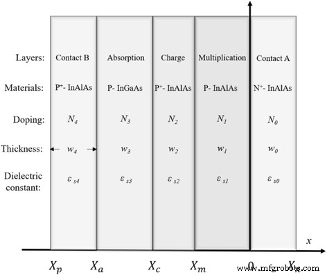
SACM InGaAs / InAlAsAPDの簡略化された数学的座標系。理論モデルを構築するために使用されるAPDの簡略化された構造を示します。基本的な構造パラメータ(材料、厚さ、ドーピング、誘電率)を含むAPDの簡略化された数学的座標系
式1はポアソン方程式であり、電荷密度ρを使用して電位分布を解くことができます。 。この式では、ρ ドーパントイオン N に等しい 空乏層モデルでは、 w は空乏層の厚さに等しく、ε は材料の誘電率です。一般的なPN接合電界分布モデルでは、ρ 空乏層の厚さに依存する変数です w およびドーパントイオン N 。このモデルでは、トンネル効果を考慮して変化します。ただし、トンネル効果を検討する前に、まず一般的な方法を使用して電界分布を作成しました。
$$ \ frac {d \ xi} {d x} =\ frac {\ rho} {\ varepsilon} =\ frac {q \ times N} {\ varepsilon} $$(1)デバイスパラメータを使用してポアソン方程式を解くことにより、最大電界の数式が得られます。この式は、式2および3に示されている空乏層の浸透厚さの変化によって決定されます。この式では、ドーピングレベル( N )、空乏層の厚さ( w )、および誘電率(ε) さまざまなレイヤーが図1にあります。
$$ {\ xi} _ {\ max(w)} ={\ sum} _ {k =1} ^ 4 \ left(-\ frac {q \ times {N} _k \ times {w} _k} {\ varepsilon_ {sk}} \ right)$$(2)$$ {\ xi} _ {\ max(w)} =\ frac {q \ times {N} _0 \ times {w} _0} {\ varepsilon_ {s0 }} $$(3)次に、式4および5を使用して、すべての点で電界分布を導出できます。境界条件は、組み込み電位 V を無視します。 br 式6で;したがって、空乏層の厚さとバイアス電圧の数学的関係を計算できます。
$$ {\ xi} _ {\ left(x、w \ right)} ={\ xi} _ {\ max(w)} + {\ sum} _ {k =1} ^ 4 \ left(\ frac { q \ times {N} _k \ times \ left | x \ right |} {\ varepsilon_ {sk}} \ right)\ left({X} _pモデルから、空乏層の境界が接触領域に達すると、式7〜11を使用して各層の電界を分析できます。実際のAPDでは、吸収層と増倍層が意図せずに真性層にドープされます。 N 3 および N 1 N 未満 2 。したがって、式9は式12とほぼ同じです。これが、電荷層がデバイス内の電界分布を制御できる理由です。
$$ {\ displaystyle \ begin {array} {l} \ xi \ left(x、{V} _ {\ mathrm {bias}} \ right)={\ xi} _ {\ max \ left({V} _ {\ mathrm {bias}} \ right)} + \ frac {q \ times {N} _1 \ times {w} _1} {\ varepsilon_ {s1}} + \ frac {q \ times {N} _2 \ times { w} _2} {\ varepsilon_ {s2}} + \ frac {q \ times {N} _3 \ times \ left | x- {X} _c \ right |} {\ varepsilon_ {s3}} \\ {} \ kern4em \ approx {\ xi} _ {\ max \ left({V} _ {\ mathrm {bias}} \ right)} + \ frac {q \ times {N} _2 \ times {w} _2} {\ varepsilon_ { s2}} \ left({X} _ {\ mathrm {c}} \ ge x \ ge {X} _a \ right)\ end {array}} $$(12)式8では、乗算と吸収の電界差は、 N の積を使用して決定されます。 2 および w 2 。 N 2 は電荷層のドーピングレベルであり、 w 2 は電荷層の厚さです。 InGaAs / InAlAs APDで適切な電界分布を得るには、吸収層(InGaAs)の電界が50〜180 kV / cmの間隔値内にある必要があります。これにより、光誘起キャリアに十分な速度が確保され、トンネリング効果が回避されます。吸収層で[10]。つまり、増倍時のなだれ場は、電荷層による吸収で50〜180 kV / cmに減少するはずです。したがって、式8を使用して、最適に計算されたドーピングレベルと電荷層の厚さを見つけることができます。増倍層が200nmの場合(アバランシェフィールド E 乗算では6.7×10 5 増倍層が200nmのときのV / cm [27]);電荷層のドーピングレベルと厚さの計算値は、図2の[28,29,30,31,32,33]の結果と比較されます。理論値の領域は、実験データとよく一致しています。この結果は、増倍厚さが確実な場合に、式8を使用して電荷層のさまざまな厚さのドーピングレベルを予測できることを証明しています。
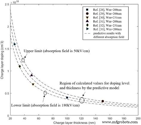
さまざまなレポートからの理論結果と実験データの比較( w m =200 nm)。閉じた記号:参照で200 nm(黒い四角、黒い円、黒い三角形、黒い右向きの三角形)と231 nm(黒いひし形、黒い下向きの三角形)の乗算厚さのドーピングレベルと電荷層の厚さ。式8による電荷層(ドーピングレベルと厚さ)の計算値を示します(吸収場は50〜180 kV / cmです)。吸収場が50kV / cmの場合、電荷層のドーピングレベルの上限を求めることができます。吸収場が180kV / cmの場合、電荷層のドーピングレベルの下限を求めることができます。さまざまなレポートの理論結果と実験データを比較します。理論値の領域は、実験データとよく一致しています。破線は、式によってドーピングレベルと厚さの計算値を計算したものです
300、500、700 nmの増倍層を使用して、電荷層のさまざまな厚さに対する最適なドーピングレベルを計算し、その結果を図3に示します。この結果は、電荷層のドーピングレベルの許容誤差がその厚さとドーピングレベルの範囲に関連して、電荷層の厚さが増加するにつれて減少します。つまり、厚い電荷領域を適用した場合、最適な電界を満たすために、電荷層にわずかな範囲のドーピングレベルしか存在しません。その結果、APDの性能は、より厚い電荷層でのドーピング濃度の数パーセントの偏差によって大幅に変化します。 「結果と考察」のセクションでは、APDの実際の構造をシミュレートして、理論分析を研究および検証しました。これには、電荷層のドーピングレベル範囲に対する電荷層の厚さの影響と、さまざまな電荷層の厚さに対するさまざまな性能が含まれます。 APD。
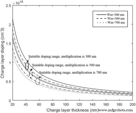
異なる増倍層に最適なドーピングレベルと電荷層の厚さ。実線: w m =300nm。破線: w m =500nm。点線: w m =700nm。吸収層の電界が適切である間、式によって電荷層の計算値(ドーピングレベルと厚さ)を示します。増倍層の厚さは300、500、700nmです。増倍層の厚さが一定の場合、式を使用して最適なドーピングレベルと電荷層の厚さを見つけることができます
トンネリングを考慮した理論モデル
上記の解析モデルは、デバイス内の電界分布に関するものであり、ρという前提に基づいています。 空乏層のドーパントイオンです。吸収層内に十分に高い電界が存在する場合、電子がトンネリングするのに十分な局所的なバンドベンディングが存在する可能性があります[34]。したがって、電子トンネリングが発生する可能性があります。図4のトンネリング概略図から、吸収層に破壊トンネリングがある場合、トンネリング効果によって電荷密度が変化しますρ 、吸収の正電荷が増加し、増倍層と電荷層の負電荷が増加します。したがって、ρ トンネル効果が現れる間、空乏層のドーパントイオン電荷密度に等しくありません。前に説明した式は、トンネリング効果を考慮した後に変更されます。
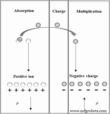
増倍層と吸収層におけるトンネリングプロセスと電荷密度の変化。デバイスのトンネリングプロセスの概略図を示します。吸収層内に十分に高い電界が存在する場合、局所的なバンドの曲がりは、電子がトンネリングするのに十分である可能性があります。吸収層にブレークダウントンネリングがある場合、吸収の正電荷が増加し、増倍層と電荷層の負電荷が増加します。したがって、ρ トンネル効果が現れる間、空乏層のドーパントイオン電荷密度と等しくありません
生成率 G bbt バンド間トンネルの概要は、式13 [35、36]で説明されています。
$$ {G} _ {bbt} ={\ left(\ frac {2 {m} ^ {\ ast}} {E_g} \ right)} ^ {1/2} \ frac {q ^ 2 {E_p} ^ {\ gamma}} {{\ left(2 \ pi \ right)} ^ 3 {\ hbar} ^ 2} \ exp \ left(\ frac {-\ pi} {4 {q \ mathit {\ hbar E}} _p} {\ left(2 {m} ^ {\ ast} \ times {E_g} ^ 3 \ right)} ^ {\ raisebox {1ex} {$ 1 $} \!\ left / \!\ raisebox {-1ex} {$ 2 $} \ right。} \ right)=A \ times {E_p} ^ {\ gamma} \ times \ exp \ left(-\ frac {B} {E_p} \ right)$$(13)式13では、 E g はInGaAsのエネルギーバンドギャップ、 m * (0.04 m に等しい e )は、有効換算質量 E p は吸収層の破壊電界であり、γ はユーザー定義可能なパラメーターであり、通常は1〜2に制限されています。 A および B 特性パラメータです。 G を計算します bbt 異なるγ 、結果を図5に示します。 G bbt γの間、電荷層のドーピングレベルに同じ桁数を適応させます 1〜1.5に制限されています。
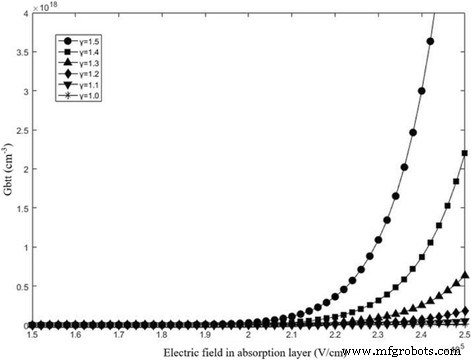
G btt 異なるγを持つ吸収層の異なるフィールドに対して 。 γの値 1.0(黒い星)、1.1(黒い下向きの三角形)、1.2(黒いひし形)、1.3(黒い三角形)、1.4(黒い四角)、1.5(黒い円)です。 G の計算結果を表示します btt 式13による。吸収場が19kV / cmを超える場合、 G bbt 徐々に増加します。 G bbt γの間、電荷層のドーピングレベルに同じ桁数を適応させます 1〜1.5に制限されています
その結果、電荷密度ρ は変数であり、トンネル効果と吸収トンネル内のドーパントイオンによって決定されます。このとき、フォーミュラ1はフォーミュラ14に変更され、増倍層の電界はフォーミュラ15で記述されます。 w トンネル トンネリングプロセスの効果的な空乏層です[35]。したがって、アバランシェフィールドの変化は式16で表すことができ、アバランシェフィールドはトンネル効果との乗算で減少します。
$$ \ frac {d \ xi} {dx} =\ frac {\ rho} {\ varepsilon} =\ frac {q \ times \ left(N + {G} _ {btt} \ right)} {\ varepsilon}、 {E} _p> 1.8 \ times {10} ^ 5V / cm $$(14)$$ \ xi \ left(x、{V} _ {\ mathrm {bias}} \ right)={\ xi} _ { \ max \ left({V} _ {\ mathrm {bias}} \ right)} + \ frac {q \ times \ left({N} _1 \ times \ left | x \ right | + {G} _ {bbt } \ times {w} _ {\ mathrm {tunnel}} \ right)} {\ varepsilon_ {s1}} \ left(0 \ ge x \ ge {X} _m \ right)$$(15)$$ \ delta \ xi \ left(x、{V} _ {\ mathrm {bias}} \ right)=\ delta E =\ frac {q \ times {G} _ {btt} \ times {w} _ {\ mathrm {tunnel }}} {\ varepsilon _ {\ mathrm {s} 3}} $$(16)電子と正孔のイオン化係数は、[18]の式17と18で表されます。 E 乗算のなだれフィールドです。
$$ \ alpha ={a} _n {e} ^ {\ raisebox {1ex} {$-{b} _n $} \!\ left / \!\ raisebox {-1ex} {$ E $} \ right。} $$(17)$$ \ beta ={a} _p {e} ^ {\ raisebox {1ex} {$-{b} _p $} \!\ left / \!\ raisebox {-1ex} {$ E $ } \ right。} $$(18)キャリアアバランシェの影響は、衝突電離モデルによって説明されます。電荷層と比較して増倍層のキャリア密度が非常に低いことを考慮すると、電界は増倍層全体で均一であると想定するのが妥当です。したがって、増倍率( M n )は次の式で表すことができます。 19.ここで、 w m は増倍層の厚さであり、 k α/βで定義される衝突電離係数比です。 。 k 以降 電界によって非常にゆっくりと変化します k w のわずかな変動に対してほぼ一定です m [37]。
$$ {M} _n =\ frac {k-1} {k \ times {e} ^ {-\ alpha \ left(1- \ raisebox {1ex} {$ 1 $} \!\ left / \!\ raisebox { -1ex} {$ k $} \ right。\ right){w} _m} -1} $$(19)定数 w を想定 m バイアス電圧、 M の微分 n 電子イオン化係数に関しては、式20および21にあります。
$$ \ delta {M} _n \ left | {} _ {w =const \&V =const} \ right。={M_n} ^ 2 {e} ^ {-\ alpha \ left(1- \ raisebox {1ex} {$ 1 $} \!\ left / \!\ raisebox {-1ex} {$ k $} \ right。\ right){w} _m} \ times {w} _m \ delta \ alpha $$(20)$$ \ delta \ alpha =\ frac {\ delta \ alpha} {\ delta E} ={\ alpha} _n {b} _n {e} ^ {\ frac {-{b} _n} {E}} \ frac {1 } {E ^ 2} $$(21)式20および21では、δα/δE 正です。全枯渇吸収層の20%が w であると想定されます。 トンネル 吸収層の厚さは400nmです。式16を解くことにより、δE間の関係 異なるγの吸収場 を図6に示します。δEであることがわかります。 乗算のアバランシェフィールドに同じ桁数を適応させます。したがって、トンネル効果は雪崩場と M に影響を及ぼします。 n トンネリング効果により減少します。解析では、負電荷は乗算で乗算されないことを前提としており、モデルはそれを考慮した後、より厳密になります。 APDの実際の構造に対するトンネル効果の影響を検証および分析するために、「結果と考察」セクションでトンネル効果と増倍なだれ場の関係を詳細にシミュレートしました。
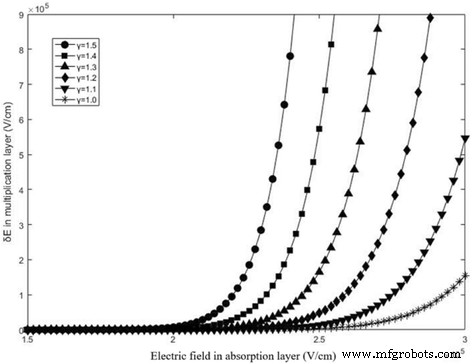
δE 異なるγを持つ吸収層の異なるフィールドに対して 。 γの値 1.0(黒い星)、1.1(黒い下向きの三角形)、1.2(黒いひし形)、1.3(黒い三角形)、1.4(黒い四角)、1.5(黒い円)です。 δEの計算結果を表示します 式16による。吸収場が19kV / cmを超える場合、δE 徐々に増加します。 δE 乗算のアバランシェフィールドに同じ桁数を適応させます。したがって、トンネル効果は、トンネル効果とともに雪崩場に影響を及ぼします
構造とシミュレーションモデル
シミュレーションと分析には、TCADの半導体デバイスシミュレーションを使用しました。このシミュレーションエンジンはシミュレーションで物理モデルを定義し、結果には物理的な意味があります[20]。基本的な物理モデルは次のように提示されました。ポアソン方程式とキャリア連続方程式を含むドリフト拡散モデルを使用して、電界分布と拡散電流I DIFF をシミュレートしました。 。バンド間トンネリング電流I B2B には、バンド間トンネリングモデルが使用されました。 、およびトラップ支援トンネルモデルは、トラップ支援トンネル電流I TAT に使用されました。 。生成-再結合電流I GR Shockley–Read–Hall再結合モデル、およびAuger再結合電流I AUGER によって記述されました。 Auger組換えモデルによって記述されました。暗電流はこれらのメカニズムによって明確に説明されました[38]。雪崩の増加は、Selberherr衝突電離モデルによって記述されました。シミュレーションモデルには、フェルミディラックキャリア統計、キャリア濃度依存、低磁場移動度、速度飽和、レイトレーシング法などの他の基本モデルが使用され、厳密なシミュレーションモデルが構築されました。
シミュレーションのデバイス構造は、[13]の実験構造と同様でした。上から照らされたSAGCMInGaAs / InAlAs APDの概略断面図を図7に示します。上から下への構造は、InGaAs接触層、InAlAsクラッド層、InAlGaAsグレーディング層、InGaAs吸収層、InAlGaAsグレーディングと順番に名付けられています。層、InAlAs電荷層、InAlAs増倍層、InAlAsクラッド層、InP接触層、およびInP基板。各層の厚さとドーピングも図7に示されています。シミュレーション結果への厚さの影響を避けるために、2つのシミュレーション構造を選択します。 1つのシミュレーション構造はAPD-1(乗算層と吸収層はそれぞれ800nmと1800nm)と呼ばれ、もう1つのシミュレーション構造はAPD-2(乗算層と吸収層はそれぞれ200nmと600nm)と呼ばれます。
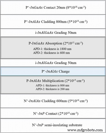
APDのシミュレーション構造とパラメータ。上部に照らされたSAGCMInGaAs / InAlAsAPD-1およびAPD-2の概略断面図を示します。構造、材料、ドーピング、厚さが含まれます
シミュレーションモデルをテストするために、[13]の実験データをシミュレーション結果と比較しました。このシミュレーションでは、リファレンスで同じ構造を使用し、デバイスの電流-電圧特性を示しました。図8は、シミュレーション結果とリファレンスの実験結果を示しています。それらは同様のパンチスルー電圧 V を持っています pt および絶縁破壊電圧 V br 。さらに、シミュレーションと実験結果はよく一致しています。したがって、シミュレーションのモデルは正確です。上記のパラメータを表1に示します。
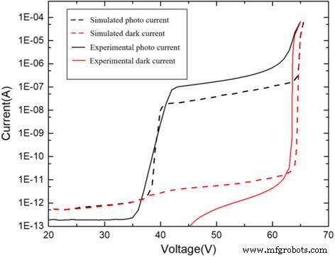
シミュレーション結果と実験結果(光電流および暗電流)の比較。黒の破線:シミュレートされた光電流。赤い破線:シミュレートされた暗電流。黒の実線:実験的な光電流。赤い実線:実験的な暗電流。シミュレーション結果と実験結果の比較を示します。シミュレーションモデルは、リファレンスの実験と同じパラメータを使用します
結果と考察
In this section, the theoretical analysis and conclusions were studied by simulation in details. First, the influence of charge layer thickness on doping level tolerance in charge layer was studied in the “Influence of Charge Layer Thickness” section. Then, relationship between the tunneling effect and multiplication avalanche field was analyzed and verified in the “Tunneling Effect on the Electric Field Distribution” section.
Influence of Charge Layer Thickness
From [14], a suitable field distribution in InGaAs/InAlAs APD should comply with those rules. The guarantee V pt < V br および V br − V pt should have a safety margin for processing variations in temperature fluctuations and operation range. In the absorption layer, the electric field should be larger than 50–100 kV/cm to ensure enough velocity for the photo-induced carriers. Concurrently, the electric field must be less than 180 kV/cm to avoid the tunneling effect in the absorption layer. Electric field distribution greatly influences the device performance. The choice of electric field in the absorption layer has a balancing of the tradeoff between small transit time, dark current, and high responsivity for the practical requirement.
In the simulation, we used the structure of APD-1 (multiplication is 800 nm thick) and adjusted the charge layer thickness from 50 to 210 nm to study the influence of charge layer thickness on doping level range and verify the theoretical conclusions in analytical model. In the simulation, we selected different doping level ranges in the charge layer so that the electric field distribution complies with the rules. The simulation results on the relationship between thickness and doping level range in the charge layer are presented in Fig. 9a. As the charge layer thickness increases, the suitable doping level range in charge layer decreases. A relatively large doping level range exists in the thin charge layer, and under this doping level range, the device will have a suitable electric field distribution. Apparently, the doping level range is determined by charge layer thickness. The simulation result of APD-2 (with a thickness of multiplication of 200 nm) is presented in Fig. 9b, which has a similar result. Moreover, it can be found that the calculated results of Fig. 2 and simulation results of Fig. 9b match well as shown in Fig. 9c. The small difference between the calculated results and simulation results is caused by the different values of avalanche field in the simulation and calculation. The avalanche field in simulation engine is used 6.4 × 10 5 V/cm, while in the calculation, we use the value of 6.7 × 10 5 V/cm from [27].

a Relationship between suitable doping level and thickness of charge layer (APD-1). The thickness of charge layer is 50 nm (black square), 90 nm (black circle), 130 nm (black triangle), 170 nm (black down-pointing triangle), 210 nm (black diamond). a presents the suitable doping level region for different thickness of charge layer. As the charge layer thickness increases, the suitable doping level range in the charge layer decreases. A relatively large doping level range exists in the thin charge layer, and under this doping level range, the device will have a suitable electric field distribution. Apparently, the doping level range is determined by charge layer thickness. b Relationship between suitable doping level and thickness of charge layer (APD-2). The thickness of charge layer is 50 nm (black square), 70 nm (black circle), 90 nm (black triangle), 110 nm (black down-pointing triangle), 130 nm (black diamond), and 150 nm (black pentagon). The figure description of b is similar to a 。 c Comparison of calculated results in Fig. 2 and simulated results in Fig. 9b. Dashed line:calculated results. Closed symbols:simulated results (black square). c presents the comparison of calculated results in Fig. 2 and simulated results in Fig. 9b. The calculated results and simulated results correspond well
The charge layer thicknesses of 210 and 50 nm (APD-1) were selected to show the simulation details and the influence of doping level on the electric field distribution. Figure 10a, c shows the current simulation results of different doping levels in thicknesses of 210 and 50 nm, respectively. Figure 10b, d shows the electric field distribution simulation results using the same structure. The simulation results show that thicknesses of 210 and 50 nm have doping level ranges of 1.0 × 10 17 –1.3 × 10 17 cm -3 and 3.9 × 10 17 –5.7 × 10 17 cm -3 それぞれ。

a Photocurrent and dark current with different doping level (thickness of charge layer is 210 nm). Solid line:doping level in the charge layer is 1.3 × 10 17 cm -3 。 Dashed line:doping level in charge layer is 1.15 × 10 17 cm -3 。 Dashed dot line:doping level in charge layer is 1.0 × 10 17 cm -3 。 a Presents the simulation results of currents with different doping level. The device with a charge layer thickness of 210 nm only has a relatively narrow and suitable doping level. A minimal change in the doping level has greatly influence the punch-through voltage, breakdown voltage, and current-voltage characteristic. b Avalanche field with different doping level (thickness of charge layer is 210 nm). Solid line:doping level in charge layer is 1.3 × 10 17 cm -3 。 Dashed line:doping level in charge layer is 1.15 × 10 17 cm -3 。 Dashed dot line:doping level in charge layer is 1.0 × 10 17 cm -3 。 b Presents the simulation results of fields with different doping level. The device with a charge layer thickness of 210 nm only has a relatively narrow and suitable doping level. A minimal change in the doping level has greatly influenced the electric field distribution. c Photocurrent and dark current with different doping level (thickness of charge layer is 50 nm). Solid line:doping level in charge layer is 5.7 × 10 17 cm -3 。 Dashed line:doping level in charge layer is 4.8 × 10 17 cm -3 。 Dashed dot line:doping level in charge layer is 3.9 × 10 17 cm -3 。 c Presents the simulation results of currents with different doping level. The device with a charge layer thickness of 50 nm has a relatively wide and suitable doping level. A minimal change in the doping level has a small influence on the current-voltage characteristic. d Avalanche field with different doping level (thickness of charge layer is 50 nm). Solid line:doping level in charge layer is 5.7 × 10 17 cm -3 。 Dashed line:doping level in charge layer is 4.8 × 10 17 cm -3 。 Dashed dot line:doping level in charge layer is 3.9 × 10 17 cm -3 。 d Presents the simulation results of fields with different doping level. The device with a charge layer thickness of 50 nm only has a relatively wide and suitable doping level. A minimal change in the doping level has a small influence on the electric field distribution
Clearly, the device with a charge layer thickness of 210 nm only has a relatively narrow and suitable doping level. A minimal change in the doping level has greatly influence the current-voltage characteristic and electric field distribution. As a result, the performance of APD varies significantly via several percent deviations of doping concentrations in the thicker charge layer. This conclusion is the same as the theoretical analysis. Concurrently, when designing APD structures, choosing a thin charge layer will give a high level of doping tolerance, as well as confer APD with good controllability.
Finally, the relationship between charge layer and multiplication thickness was simulated. Figure 11a presents the avalanche field with multiplication region thicknesses of 100, 200, and 300 nm in the APD-2 structure (with a charge layer thickness of 70 nm). Figure 11b presents the charge layer doping range with different multiplication thicknesses at the suitable electric field distribution condition. The charge layer thicknesses are 50, 70, and 90 nm. Clearly, a high avalanche field exists in the thin multiplication layer. As the multiplication region thickness decreases, the electric field difference between multiplication and absorption layers increases. As a result, a thin multiplication layer needs a high product of the charge layer doping level and thickness to reduce the high avalanche field.

a Avalanche breakdown electric field with different multiplication thicknesses. Solid line:w m = 100 nm. Dashed line:w m = 200 nm. Dashed dot line:w m = 300 nm. a Presents the simulation results of electric field distribution with different w m 。 As the w m decreases, the avalanche field in the multiplication increase. b Relationship between multiplication thickness and charge layer. The thickness of multiplication is 300 nm (black square), 200 nm (black circle), 100 nm (black triangle). b Presents the relationship between multiplication thickness and charge layer. A thin multiplication layer needs a high product of the charge layer doping level and thickness to reduce the high avalanche field
Tunneling Effect on the Electric Field Distribution
The simulation in this part will study the tunneling effect on the electric field in the device. From the theoretical analysis, the tunneling effect has an influence on the avalanche field in multiplication. Thus, the simulation will design to study the influence of electric field in the absorption layer that exceeds the tunneling threshold value. First, group A, with the structure of APD-1, charge layer thickness of 90 nm, and different charge layer doping levels of 1.4 × 10 17 –2.4 × 10 17 cm -3 , was simulated for electric field distribution when the device avalanche breaks down. The result is shown in Fig. 12a. When the charge layer doping level exceeds 2.0 × 10 17 cm -3 , the field in the absorption layer becomes lower than the tunneling threshold field and the avalanche field in the multiplication layer reaches the same value. However, when the doping level is less than 2.0 × 10 17 cm -3 , the field in the absorption layer exceeds the tunneling threshold field and the avalanche field in the multiplication layer decreases with the decrease of the doping level in charge layer. Similar results were observed in the APD-2 structure (with a charge layer thickness of 90 nm and doping level of 2.2 × 10 17 –3.6*10 17 cm -3 ) (Fig. 12b). That is, if the electric field in the absorption layer exceeds the tunneling threshold value at or over the breakdown voltage, then the breakdown electric field in the multiplication will decrease.

a Avalanche breakdown electric field with different doping levels (APD-1). Thickness of charge layer is 90 nm. Red dashed lines:the field of absorption is larger than the tunneling threshold field. Black solid lines:the field of absorption is less than the tunneling threshold field. a Presents the simulation results of electric field distribution with different doping level while avalanche breakdown. When doping level of charge layer exceeds 2.0 × 10 17 cm -3 , the field in the absorption layer becomes lower than the tunneling threshold field, and the avalanche field in the multiplication layer reaches the same value with different doping level. However, when the doping level is less than 2.0 × 10 17 cm -3 , the field in the absorption layer exceeds the tunneling threshold field, and the avalanche field in the multiplication layer decreases with the decrease of the doping level. Thus, if the electric field in the absorption layer exceeds the tunneling threshold value at or over the breakdown voltage, then the breakdown electric field in the multiplication will decrease. Thus, the electric field in the absorption should be less than the tunneling threshold value to maintain the high field in the multiplication layer when the device avalanche breaks down. b Avalanche breakdown electric field with different doping levels (APD-2). Thickness of charge layer is 90 nm. Red dashed lines:the field of absorption is larger than the tunneling threshold field. Black solid lines:the field of absorption is less than the tunneling threshold field. The figure description of b is similar to a 。 c Relationship between field and bias voltage in multiplication and absorption (APD-1). Thickness of charge layer is 90 nm. Electric field of multiplication (black square). Electric field of absorption (red triangle). c Presents the relationship between the electric field and bias voltage in multiplication and absorption layers. When the electric field in the absorption layer reaches the tunneling threshold value, the avalanche breakdown electric field in the multiplication gradually decreases. Moreover, the absorption field slope increases when the electric field in the absorption layer exceeds the tunneling threshold. d Relationship between field and bias voltage in multiplication and absorption (APD-2). Thickness of charge layer is 90 nm. Electric field of multiplication (black square). Electric field of absorption (red triangle). The figure legend of d is similar to a
Groups B (APD-1 thickness of 90 nm, doping level of 2.4 × 10 17 cm -3 in charge layer and APD-2 thickness of 90 nm, doping level of 3.6 × 10 17 cm -3 ) were designed to demonstrate the relationship between the threshold electric field in the absorption layer and avalanche field in the multiplication layer. The multiplication and absorption electric fields vary with the bias voltage on the device. As shown in Fig. 12c, d, when the electric field in the absorption layer reaches the tunneling threshold value, the avalanche breakdown electric field in the multiplication gradually decreases. Moreover, when the absorption field exceeds the tunneling threshold, the avalanche breakdown electric field in the multiplication layer plummets. Furthermore, the absorption field slope increases when the electric field in the absorption layer exceeds the tunneling threshold.
The phenomenon in Fig. 12 can be explained by the theoretical analysis that tunneling has an influence on the charge density in the “Methods” section. When the electric field reaches the tunneling threshold value in the absorption layer, the charge density ρ becomes unequal to the dopant ion. The multiplication field will decrease as the negative ion increases, and the absorption field will increase as the positive ion increases. Concurrently, the absorption field slope will increase due to the tunneling effect. As a result, the electric field in the absorption should be less than the tunneling threshold value to maintain the high field in the multiplication layer and the low dark current when the device avalanche breaks down.
結論
In summary, we have presented a theoretical study and numerical simulation analysis involving the InGaAs/InAlAs APD. The mathematical relationship between the device parameters and electric field distribution in the device was built. And the tunneling effect was taken into consideration in the theoretical analysis. Through analysis and simulation, the influence of structure parameters on the device and the detailed relationship of each layer were fully understood in the device. Three important conclusions can be obtained from this paper. First, the doping level and thickness of the charge layer for different multiplication thicknesses can be calculated by the theoretical model in the “Methods” section. Calculated charge layer values (doping and thickness) are in agreement with the experiment results. Second, as the charge layer thickness increases, the suitable doping level range in charge layer decreases. Compared to the thinner charge layer, the performance of APD varies significantly via several percent deviations of doping concentrations in the thicker charge layer. When designing APD structures, choosing a thin charge layer will give a high level of doping tolerance, as well as confer APD with good controllability. Finally, the G btt of tunneling effect was calculated, and the influence of tunneling effect on the avalanche field was analyzed. We confirm that the avalanche field and multiplication factor (M n ) in the multiplication will decrease by the tunneling effect.
略語
- 2D:
-
二次元
- APD:
-
Avalanche photodiode
- DCR:
-
Dark count rate
- SACM APDs:
-
Separate absorption, charge, and multiplication avalanche photodiodes
- SAGCMAPDs:
-
Separate absorption, grading, charge, and multiplication avalanche photodiodes
- SPAD:
-
Single-photon avalanche photodiode
- SPDE:
-
Single-photon detection efficiency
- SRH:
-
Shockley–Read–Hall
ナノマテリアル
- マイクロLEDおよびVCSEL用の高度な原子層堆積技術
- 電子増倍管の発光層の設計
- プラズマ化学原子層堆積によって調製されたCo3O4被覆TiO2粉末の光触媒特性
- 二軸引張ひずみゲルマニウムナノワイヤの理論的研究
- 界面層の設計によるZnO膜の表面形態と特性の調整
- 超循環原子層堆積によるZnO膜のフェルミ準位調整
- 後部に黒色シリコン層を備えた結晶シリコン太陽電池の調査
- 1.3〜1.55μmウィンドウでの変成InAs / InGaAs量子ドットのバンド間光伝導
- 低エネルギー照射に対するSi、Ge、およびSi / Ge超格子の放射応答の理論的シミュレーション
- InGaAs / InPコアシェルナノワイヤの自己シードMOCVD成長と劇的に増強されたフォトルミネッセンス
- 固体ソース2段階化学蒸着によって生成されたInGaAsナノワイヤの形成メカニズム