


5 nmデトネーションナノダイヤモンドのNV-中心からのフォトルミネッセンス:同定と磁場に対する高感度
要約
窒素空孔の含有量(NV - )窒素含有爆薬の爆発中に生成されたナノダイヤモンド(DND)の色の中心は、1.1±0.3ppmであることがわかりました。この値は、意図的に作成されたNV − を備えたサイズ<10nmのナノダイヤモンドにとって印象的です。 センター。濃度は、 g の積分強度から決定された電子常磁性共鳴から推定されました。 =4.27行。この行は「禁止」に関連しています∆ m s =2NVのゼーマンレベル間の遷移 − センターの地上三重項状態。共焦点蛍光顕微鏡は、NV - の赤色フォトルミネッセンス(PL)の検出を可能にします 5nmナノ粒子から形成されたナノスケールDND凝集体の色の中心。 NV - で構成されるサブ波長エミッタ 回折限界スポットの数分の1のサイズで明確に区別されます。さらに、NV - で、基底状態と励起状態のスピンレベルを混合および反交差すると、PL強度の急激な低下が観察されました。 印加された外部磁場の下で発生します。この効果は、NV − のユニークな量子機能です。 中心。これは、ダイヤモンド格子内の他の可視領域の発光色の中心では観察できません。
背景
窒素空孔(NV - )を含む蛍光ナノダイヤモンド(ND) )センターは、革新的なアプリケーションへの道を開く新しいナノマテリアルです。特定のアプリケーションには、現在、磁気センシング[1]、バイオイメージング[2]、およびナノ共振器結合光子源の使用を含む電気通信および情報処理が含まれます[3、4]。 NV - の前例のない独自の量子特性から、幅広い応用分野が生まれます。 室温で発生するカラーセンター。カラーセンターは、光学的に検出可能な磁気共鳴(ODMR)によって検出できる三重項スピン特性を持っています[5]。ナノダイヤモンドの蛍光特性とその小さなサイズ(<40 nm)を組み合わせることで、サブミクロンの細胞小器官の細胞内コントラストイメージングや胚のナノメートルスケールの温度測定などの生物医学アプリケーションでの使用が可能になります[6、7、8]。生体適合性のある半透明のシェルにナノダイヤモンド微結晶をカプセル化することは、生物学的環境での応用に特に有望です[9]。また、金属のジョンソンノイズを測定するための点状プローブとしても使用できます[10]。ナノダイヤモンドは、爆発物の爆発中に生成され、いわゆるデトネーションナノダイヤモンド(DND)を生成します。ただし、DNDには通常、高濃度の欠陥が含まれています。これにより、たとえば、磁気センシングアプリケーションやナノスケールでの他のローカルプロービングでのDND(サイズ<6 nm)のアプリケーションが制限されます[11]。
DNDは、爆発中の爆発物のエネルギー放出成分の熱分解生成物から合成されます。爆発物と爆発は、貯水池の中に含まれています。合成は、たとえば、最大10cmのサイズの爆発物のブロックの爆発中に13〜20μsの期間に行われます。今回は、爆発波が爆発ブロック全体に伝播するのにかかる時間です。ただし、個々の爆発性微小顆粒は、はるかに短い時間(<0.1μs)で分解およびガス化します。炭素と窒素は爆発性物質の主成分です。デトネーション中に、最大5 nmのサイズのダイヤモンド微結晶が、爆発性成分、つまり主に炭素の分解生成物から自己組織化されます。窒素はまた、合成中にダイヤモンド格子に組み込まれます。 CH 3 の存在 *気相分解生成物中のラジカルは、複雑なC–N–O–Hガス環境で急速なダイヤモンド格子集合を引き起こします。ガス環境はマイクロ秒スケールで変化し、圧力の除荷が速く、温度が下がると、炭素のР–Т状態図でダイヤモンドの合成と安定性に必要な領域に対応する環境条件が得られます[12]。
凝縮中心でのダイヤモンド微結晶の非常に迅速な集合(および非ダイヤモンド形態のアモルファスカーボン)は、成長する格子内で先験的に異なる形態の多数の欠陥、空孔、および複数の空孔の出現を引き起こします。空孔は、ダイヤモンド格子の迅速な組み立て中に発生する積層欠陥と不正確さの結果として自然に存在します。爆轟中の最高温度から800〜900℃までの温度低下中、空孔は依然として格子内を移動する可能性があります。したがって、空孔はクラスターに結合するか、微結晶の表面で消失する可能性があります。合成のこの段階での空孔の移動性により、置換窒素原子による空孔の捕捉も可能になります。同じプロセスが窒素不純物にも適用されますが、唯一の違いは、孤立した窒素置換が1600°C未満の温度では格子内で実質的に動かないため、高温でのみ凝集することです。窒素不純物は、さまざまな形でDNDの格子内に存在する可能性があります。それは、最大〜2.5 at。%の量の凝集形態(A中心、二量体)または単離された炭素置換原子(C中心)の形態で存在することができます。よく知られているように、A中心は非常磁性でスピンゼロですが、スピン半分のC中心は中性型(P1中心)で常磁性です。したがって、P1中心は、電子常磁性共鳴(EPR)法によって簡単に検出できます。負に帯電している格子の空孔(V - )、常磁性ですが、スピン3/2があります。スピンハーフスピンは、一般的な量のDNDで見つかりました[13]。 EPR法で検出されたスピンハーフラジカルの濃度は実質的に同じです(1100–1400 ppm) 脚注1 工業生産のすべての標準DNDで。これは、特定の商業生産者や技術の詳細に関係なく、細部が異なる場合があります。スピンハーフラジカル濃度は、粒子重量(またはその中の対応する炭素原子の数)と比較した、DND粒子内のダングリングボンドスピンを有する置換窒素原子および他の欠陥の総数のほぼ合計です。 DNDの窒素の大部分(最大〜2.5 at。%)は、ダイヤモンドコアの共有結合格子にほぼ均一に分布していますが、積層欠陥などの欠陥領域で濃縮されています[14、15]。また、ターナーらによって結論付けられました。埋め込まれた窒素は、主にN–N二量体(A中心)または孤立した中性、正または負に帯電した窒素の形でダイヤモンド格子に存在します sp 3 -配位不純物(C中心)[14、15]。したがって、DNDの窒素のほとんどは、ダイヤモンド結晶格子の隣接するノードにある非常磁性の窒素ペア(N–N)です。
一般的な窒素不純物に加えて、DND粒子には、孤立した空孔、複数の空孔、窒素-空孔-窒素(NVN)および窒素-空孔(NV)タイプの欠陥中心も含まれています。これらの追加の欠陥中心は、格子アセンブリ中に隣接する格子サイトに構成剤が自発的に出現するために発生します[11]。同時に、負に帯電したNV - の存在 サイトは主に、システム内で電子供与体の役割を果たす過剰な中性窒素原子からの負電荷を帯電させて受け入れるためです。予備的なEPRデータによると、NV - の濃度 g を使用してEPRラインの積分強度から決定できる中心 -半磁場での4.26〜4.27の係数は、分離された置換窒素の濃度よりも約2.5〜3桁小さく、400〜700ppmの値になります。
マルチバカンシーとNV − センターは、以前の最近の研究[13、16、17]でEPR法によってDNDで正常に識別されました。 NVの明るさの関係を理解するための努力もなされています − DNDの中心とその表面の化学組成、環境、骨材の形態[18、19]。 NVの放出特性の制御に関する同様の作業 - 人工的に作成されたNVセンターを備えた合成蛍光ダイヤモンドに対しても行われました[20]。それにもかかわらず、X線粉末回折、EPR分光法、共焦点蛍光分光法と顕微鏡法、元素分析、回折限界サイズのエミッターの分析、フォトルミネッセンス信号への磁場の影響など、さまざまな分析方法を組み合わせた必要な研究は十分に行われていません。 NVのトピックについて − 予備作業[21]を除いて、DNDのセンター。現在、NV - の発光特性の依存性 内部不純物含有量と粒子形態に関するDNDでは理解されていません。この作業では、DND粒子がNV - の特定のフォトルミネッセンス(PL)を示すことを報告します。 センター、NVの内容を正確に数える − 洗練されたアプローチを介してそれらの中で、ダイヤモンド結晶子サイズと窒素含有量の関数としてスペクトル最大でそれらのPL強度を分析します。さらに、ODMRの特性に関連する外部磁場に対するDNDの感度を示します。
実験的
製造方法とDND形態の制御
DND粉末は、数立方メートルの密閉されたステンレス鋼容器内で、適切な厚さの水殻に囲まれたトリニトロトルエン-ヘキソゲンの爆発性混合物の約1kgの爆破を含むほぼ標準的なプロセスによって得られました。これは、いわゆる「ウェット」合成です。製品の合成と一次精製は、ロシアのサンクトペテルブルクにある特別設計技術局「SCTBTechnolog」という商業メーカーによって実施されました。この企業で使用されている技術プロセスにより、コヒーレント散乱領域(CSR)のサイズが4.5nmから約5.7nmの範囲で変化するナノ結晶子のみで構成されるDND粉末を得ることができます。標準技術によって調製されたいくつかの精製されたDND粉末は、PlasmaChem GmbH(ベルリン、ドイツ)から供給されました。供給されたままのDNDサンプルの形態は、X線回折(XRD)によって確立されました。 XRDパターンは、法政大学マイクロナノテクノロジー研究センター(東京、日本)で、D / teX Ultra検出器、CuKα放射線源(λ)を備えたRigaku SmartLab IX線回折計を使用して記録されました。 =1.54178Å)および角度範囲2Θ=5–100 o のニッケルフィルター (ステップ0.01 o )。分析の過程で、ハードウェア機能の幅が考慮されました。 X線CSRサイズは、参考文献に記載されている方法に従って、2Θ角度の関数としての111、220、および311反射の幅の高度な分析に基づいて決定されました。 [22]。 脚注2 この方法の主な特徴は、格子定数パラメーター( a o =3.5640Å)は、系統的誤差(異なるモデルの選択による変動)が±0.0003Å以下のすべてのDNDサンプルで取得できます。 X線粉末回折測定は、5.2±0.2nmのその後の研究のために選択された1つの代表的なDNDサンプルのCSRサイズを示しました。このDNDサンプルは、以下に説明するすべての主要な研究で使用されました。さらに、特別な条件下(爆発ゾーンへの無機添加剤の有無にかかわらず)で同じメーカーによって合成され、異なるX線CSRサイズを持ついくつかのDNDサンプルを使用して、フォトルミネッセンス強度とCSRサイズの依存性をプロットしました。内部窒素の含有量。通常の技術で合成されたDND粉末のCSRサイズは4.6±0.2nmでした。
DND粉末は、沸騰酸混合物でさらに精製され、3d強磁性金属の残留不純物が除去されたため、より正確なEPRおよびXPS研究が可能になりました。ラマン散乱とその後のフォトルミネッセンス研究には、空気中のDND粉末を430°Cで10〜12時間アニーリングすることによる追加の表面洗浄が必要でした[23]。酸精製して空気中で処理した後、個々の個別のナノダイヤモンド粒子と25nm未満のサイズの凝集体を含むDND粉末を分解するためのさらなる努力は行われませんでした。水懸濁液中のDND凝集体の平均サイズは25〜30nmでした。
共焦点蛍光顕微鏡研究用のサンプルは、DNDの水性懸濁液から製造されました。懸濁液は、酸精製および空気アニールした粉末を約1 mg / mlの濃度で水に分散させ、続いて水で100倍に希釈することによって得られました。次に、DND懸濁液を170μmにさらにスピンコーティングしました。 -超音波浴でエタノールとアセトンの混合物で事前に洗浄された厚いカバーガラス基板。最後に、カバーガラス基板上に堆積したDND凝集体を、UV / Oクリーナー(低圧水銀ランプ:光パワー> 25 mW / cm 2 )で洗浄しました。 λで =254 nm)約30分。紫外線にさらされると、光を吸収する sp の効率的な酸化と気相エッチングが行われます。 2 - 酸素とオゾンを含むDNDの周りの炭素が発生します。 sp の外部ナノスケールクラスター 2 -炭素は、DNDのダイヤモンド格子の固有の色中心からPLを研究するのに非常に望ましくありません。基板をUV放射にさらすと、不要な有機汚染物質が除去されます。そうしないと、広いスペクトル範囲で発光バックグラウンドが発生する可能性があります。
特性評価方法
磁気共鳴分光法
サンプルのEPRスペクトルは、EPR分光計(JEOL JES-FA 300(日本))を使用して、室温で、マイクロ波Xバンド内で〜9.4393 GHzまたは〜9.0785GHzの周波数で記録されました。使用される特定の固定周波数は、研究サイクル全体を通してマイクロ波空洞内の石英断熱クライオスタットの有無に依存していました。数十ミリグラムのDND粉末を、外径5mm、長さ100mmの石英底面を備えた長いXバンドJEOLEPRチューブ(JEOLパーツカタログ、アイテム4220 00281、No.193)に導入しました。チューブの開いた上部は湿気から密閉されていました。 JEOLEPRチューブとマイクロ波空洞の中央にあるDND粉末の写真を図1aとbに示します。灰色の粉末が両方のパネルにはっきりと見られます。このような量のDND粉末は、高いQファクターを備えたEPR分光計の効果的な調整と、半磁場領域の弱い信号のスペクトルの記録中に良好な信号対雑音比を得るのに適しています。
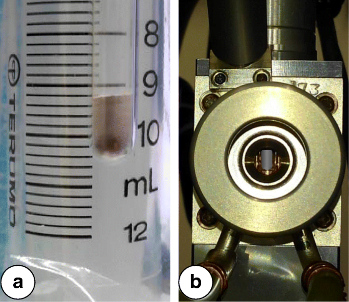
a のDNDパウダーの写真 JEOLEPRチューブと b Xバンドマイクロ波空洞の中心にあります。比較のために、EPRチューブ内の粉末の画像は、10mlの容量のプラスチック注射器の主要部分に対して特別に撮影されています
g を使用したDNDのEPRスペクトル -4.00〜4.30の範囲の信号の係数は、マイクロ波電力 P で記録されました。 MW =6 mW;磁場変調振幅、 A m =0.5 mT;頻度、ν =100 kHz;ゲイン、 G =1200;信号の蓄積、 N =20。時定数は0.030sでした。 1回の磁場掃引の記録時間は120秒でした。
スイープの最小および最大磁場値は、JEOL-JESプログラムソフトウェアで特別に選択され、JEOL NMRフィールドメーターES-FC5(Echo Electronics)で正確に定義されました。 NVの濃度 - センターは、対応するEPR信号と g の二重積分によって推定されました。 =4.27に続いて、対応するサンプルの重みに割り当て、参照サンプルからのEPR信号と比較します。合成蛍光IbHPHTダイヤモンドパウダー 脚注3 を特別に選択しました (平均サイズ〜100 nm) g の明確に定義された積分強度 =4.27EPRラインと既知の濃度 S =1 NV − 得られたNV - の濃度を正しく決定できるようにするための、独立した信頼できる基準としての5.3±0.4ppmの中心 DNDで。これは、Shamesらによって以前に提案されたアプローチに似ています。 [24]。 g =4.27EPRラインは、次のパラメータを使用してこの参照サンプルに対して記録されました: P MW =3μW、 A m =0.2 mT、 G =500、および N EPRラインのピークツーピーク強度がサンプル空間のマイクロ波パワーの平方根に比例する線形モードでは=12。サブミクロンおよびミクロンサイズのIbHPHT結晶の場合、このレジームは通常、低マイクロ波電力(7〜10μW未満)で十分に実施されます。スペクトルは、119〜321mTの広範囲の磁場で特別に記録されました。この範囲は、Δ m からの追加のEPR信号を登録するために使用されました。 s =1遷移。これは低磁場で許可され、NVの一意のシグネチャを表します − センター。
X線光電子分光法
DNDのX線光電子分光法(XPS)は、単色AlKα放射線源を備えたPerkin-Elmer PHI5600マルチテクニックシステムを使用して実行されました。光電子のスペクトル特性は、〜1 mm 2 のサンプル領域から放出された光電子束を分析した後に得られました。 [25]。検出された光電子は、材料の表面、つまり原子層の厚い領域(<2 nm)から放出されます。炭素C1、窒素N1、酸素O1の光電子放出ピークの面積の分析に特に注意が払われました。光電子放出ピークの個々の成分への分解は、適切な一重項等高線のセットによって実行されました。 DNDサンプルのスペクトルは、アルゴンイオンで表面をエッチングした後に取得しました。イオンエッチングは、加速電圧3 kV、イオンビーム電流約4μAで3分間行った。 Arイオンエッチングを使用して、吸着された周囲ガスおよびその他の化学吸着された原子錯体をサンプル表面から除去しました。 XPSは、さまざまなX線CSRサイズの一連のさまざまなDNDサンプルの内部窒素含有量を評価するためにも使用されました。
蛍光分光法
PL研究では、4mmの銅板に開けられた直径2mmの浅い穴に粉末フラッシュを押し込み、続いてガラス板で表面を平らにすることによってサンプルを準備しました。 PLスペクトルは、約0.5mWの出力で532nmのレーザー励起を使用したカスタムマイクロラマンセットアップと、1ミリメートルあたり600の溝を備えた回折格子を使用して、540〜1000nmの範囲で記録されました。露光時間は180秒でした。励起放射線は、Nikon Plan Apo 100x、NA =1.40顕微鏡対物レンズを介して、直径2μmのスポットに平坦なサンプル表面に集束されました。スペクトル分解能は0.05nmよりも優れていました。
共焦点蛍光顕微鏡
PLスペクトルを登録し、カバーガラスにスピンコートされたDND粒子からのPL信号をマッピングするために、さらにPLセットアップを使用しました。これは、イメージング分光器と組み合わせたカスタム倒立共焦点走査顕微鏡で構成されています。共焦点顕微鏡には、圧電走査ステージ(NanoPDQ75、Mad City Labs Inc.、米国)、顕微鏡対物レンズ(Plan Apo 100x、NA =1.40、ニコン、日本)、および光学励起半導体レーザー(Verdi、Coherent Inc.、 USA)二色性ビームスプリッター(z532rdc、Semrock、USA)を介して対物レンズに注入される(円偏光、0.5 mWパワー)532nmの波長で発光します。検出パスは、共焦点除去用の直径50μmのピンホール、バンドパスフィルター(FF01-697 / 75、Semrock)、および単一光子計数モジュール検出器(SPCM-AQR-14、Perkin-Elmer、カナダ)で構成されています。 。イメージング分光器は、裏面照射型CCDアレイ検出器(DU440-BU2、Andor Technologies、英国)でスペクトルをイメージングする凹面回折格子で構成されており、約1nmのスペクトル分解能が得られます。
発光シグナルのマッピングは、20×20μm 2 で実行されました。 平方。横方向の基本ステージの変位は、精度〜1nmで100nmでした。 500〜900 nmの範囲のPLスペクトルと、適切なスペクトルの最大値でのPL強度の時間依存性を取得するために、横方向のサイズが0.6ミクロン以下で強い発光を持つ基板上にあるいくつかのDND凝集体のうち2つを選択しました。 。露光時間は、各PLスペクトルで60秒、登録された各2DPLマップで1ピクセルあたり3秒でした。回折限界のスポットサイズ(点像分布関数、PSF)は、約2〜3ピクセル(250 nm)をカバーします。磁場は、カバーガラス基板から約1mm以内に配置された永久磁石を使用して適用されました。サンプル位置での磁場の強さは約90〜100mTでした。 PL信号の時間依存性は、サンプルを使用した表面への磁石の迅速な接近と表面からの磁石の除去を繰り返して記録されました。
結果と考察
NVのカウント − ハーフフィールドEPR法によるDNDの中心
カラーセンターから放出される放射線は sp によって吸収される可能性があるため 2 DND凝集体の内部に存在する種を含み、粒子間の空間の特定の形態学的特徴によってさえブロックされる可能性があるため、NVを制御および監視することが非常に重要です - 非光学的方法によるダイヤモンドの中心。 NV − 中心は、励起光放射と発光光放射の両方を遮断する不透明で高密度の媒体にキャリアを埋め込んだ場合、またはNV - がない場合でも、EPR分光法によって検出できます。 特定の消光メカニズムに関連する二次放射線。その後、それらの総濃度は、EPRスペクトルの分析によって簡単に評価できます[16、26、27]。同時に、決定されたNVの濃度 - センターは、NVの潜在的な(大規模な精製後の)明るさに関する貴重な情報を提供します - PL。いわゆる半磁場の領域で3d遷移金属磁性不純物(主にFe、Ni)から精製されたDND粉末のEPRスペクトルを図2(黒い曲線)に示します。スペクトルは、 g の2本の近い線(1と2)で構成されています -ファクター g 1 =4.27および g 2 =4.00、幅ΔH pp1 ≈2.0mTおよびΔH pp2 ≈1.4mT。最初の低力線は、禁制遷移Δ m に対応します。 s =2NVの三重項状態のゼーマンエネルギー準位の間 − 磁場の中心。 2番目の高力線は、同じ禁制遷移Δ m に対応します。 s =2、これはマイクロ波放射が他の中心、つまり S を持つ複数の空孔によって吸収されるときに発生します =1。参考文献[16]、これらの線は、最初にDNDに共存するさまざまなトリプレットセンター、特に g に割り当てられました。 1 =4.27回線がNVに割り当てられました − 中心。 g の位置 1 =4.27線は禁制遷移の線に対応Δ m s =2一重項-三重項NVの基底状態のエネルギー図に示されている - 300 mTまでの磁場の中心(図3)。スピンハミルトニアン( D =850×10 −4 cm -1 )、トリプレットNV - の構成スピンの強い交換相互作用によって引き起こされます 中央、 g の位置の高感度を引き起こします 1 =4.27行( g で0.5%シフト -スケール)9.0〜9.9 GHz(Xバンド)の範囲の特定のマイクロ波周波数に[26]。線の積分強度 g 1 =4.27を使用して、NV − の濃度を正確に推定できます。 ナノダイヤモンドの発光が、隣接する光学活性種による吸収または消光、あるいは第3の共存種からの強い寄生バックグラウンド発光によるマスキングのために検出できない場合でも、中心になります。既知の濃度のNV - を備えた、高エネルギーの電子照射された合成サブミクロンダイヤモンド(平均サイズ100 nm) センターは参照サンプルとして使用されました(サンプルIb HPHT FND)。低マイクロ波電力 P で取得されたサンプルIbHPHTFNDのEPRスペクトル MW =3μWを比較のために図2(赤い曲線)に示します。 320 mT未満の範囲では、「禁止された」Δ m に対応する3つの明確に定義されたEPR信号で構成されます。 s =2(157.85 mT)、2つは z を許可 、Δ m s =1および x 、 y 、Δ m s =1(234.39mTおよび281.27mT)は、NVの基底三重項状態のゼーマンエネルギー準位間を遷移します - 磁場中。 Δ m s =2および z 、Δ m s =1の遷移も図3のスキームに示されています。NV - を使用したサブミクロンの参照サンプルと比較すると、かなり驚くべきことです。 中心では、DND粒子は g のみを示します =4.27Δ m に関連するEPRライン s =2「禁制」遷移。特に、許可された z 、Δ m s =1および x 、 y 、Δ m s =1マイクロ波遷移は観察されません。考えられる説明は、Δ m に関連するEPR線の異常な広がりです。 s スピンハミルトニアン( D )の主なパラメータの大きな変動による=1遷移 および E ) S の場合 =1 NV − DND粒子のアンサンブル上。したがって、許可された z に関連する行が完全に存在しない 、Δ m s =1および x、y、 Δ m s =1トランジションは、NV − の重要な型破りな機能です。 DNDで。商業的供給業者によると、NVの予想濃度 - 参考文献では、吸収された照射線量に基づいて評価されたIb HPHT FNDは〜5.3ppmでした。 g の積分強度 1 =DNDのEPRスペクトルの4.27線は、Ib HPHT FND EPRスペクトルの線の約4.8分の1であることがわかりました。したがって、NVの濃度は - DNDの中心は1.1±0.3ppmであると決定されます。半磁場範囲(130〜180 mT)の両方のEPR信号とバックグラウンド補正を統合する対応する手順を、図4に特別に示します。図4 aには、一次導関数の元の測定されたEPRスペクトルが含まれています。数学的処理の前のマイクロ波吸収の(曲線1);積分後の同じEPRスペクトル(上の曲線2)。測定された元のEPRスペクトルと同じですが、残りの鉄含有錯体に関連する幅広いローレンツ型の線を差し引いた後です(下の曲線3)。図4bは、バックグラウンド補正された測定時のEPRスペクトルを積分した後の、参照サンプル(上の曲線)とDND(下の曲線)の両方のEPRスペクトルを示しています。 DND自体の真の統合スペクトル(図4b、下の曲線)は、DNDの未補正の測定されたEPRスペクトルのみが統合された図4aの2番目のスペクトルとはまったく異なります。得られたスペクトル(図4b、下の曲線)は、隣接するEPR信号( g )間の非常に深い谷を示しています。 1 =4.00および g 2 =4.27)〜10mTの距離で区切られたローレンツ型。図4のパネル(b)に示されているEPRスペクトルの下の影付きの領域は、線 g の積分強度を示しています。 1 比較した両方のサンプルで=4.27。サンプルの重みで正規化した場合のこれらの領域の比率は約〜4.8です。興味深いことに、DNDの場合、線の形状 g 1 =4.27は対称的で広いです。この線は、高磁場 g と部分的に重なっています。 2 =4.00複数の欠員によって引き起こされたEPRライン。図4a(スペクトル2)には、強力なベースライン(主に除去不可能な鉄関連の錯体から)の形で残っている未修正の背景がはっきりと見られます。したがって、130〜180 mTの範囲で少なくとも3つの重複するコンポーネントのDNDのEPRスペクトルを正しく分解することが、 g の積分強度を正しく評価するための主な必要性です。 =4.27ラインとNVの濃度 − 。また、500°C未満の温度(真空中および空気中)でのさまざまな処理は、NV - の濃度に実際的な影響を与えないこともわかりました。 DNDのセンター。信号の二重積分強度 g 1 =4.27(νの〜151mTを中心とするローレンツ輪郭の下の影の領域 =9.0785 GHz)は、治療後も以前とほぼ同じです。これは、NV - が 中心は、少なくとも格子定数(〜0.36 nm)のナノ粒子表面からの深さで、格子の十分に深く埋め込まれているため、ダイヤモンド相をエッチングまたは浸透しない外部の化学物質と反応することはできません。
>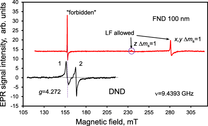
半磁場の領域での酸精製DND(黒の曲線)と、最大320mTの範囲で平均サイズが約100nm(赤の曲線)の参照電子照射蛍光IbHPHTダイヤモンドナノ粒子のEPRスペクトル。 DND EPRスペクトルの両方の線は、番号1と2でマークされています。 g の低力線1 =4.272はNV − に対応します センター。低電界(LF)に関連する線は z を許可しました Δ m s =1および x 、 y Δ m s FND 100nmの=1遷移は、上部スペクトルの矢印でマークされています。許可された z に関連する最も弱い、ほとんど区別できない線 Δ m s =1遷移はさらに円でマークされます。 The microwave frequency was 9.4393 GHz

Energy diagram of ground singlet-triplet levels 3 A 2 of NV − in magnetic field up to 300 mT. “Forbidden” Δm s = 2 and LF allowed Δm s = 1 transitions caused by absorption of microwave radiation (ν ≈ 9.44 GHz) are marked by vertical red arrows. The position of the ground state spin level anti-crossing (|0 〉GS and |−1〉GS ) is marked by a circle

a Background subtraction in EPR signal of DND and b estimations of the double-integrated intensities of the g = 4.27 line for a DND sample and reference fluorescent Ib HPHT synthetic diamond.パネル a :as-registered first derivative EPR signal of the DND in the ± 15 mT half magnetic field range (curve 1, blue); the same, but integrated EPR signal in the same ± 15 mT range of magnetic field (curve 2); the same first derivative EPR signal of DND, but after subtraction of the broad parasitic EPR signal from remaining non-removable iron-containing paramagnetic complexes shown by red contour of Lorentzian shape in the upper curve (curve 3, blue).パネル b :Estimation of the double integrated intensity of the g = 4.27 line for a fluorescent Ib HPHT diamond having NV − (upper curve, shaded area) and the DND sample (bottom curve, shadow area). The bottom spectrum in panel b consists of two contours of Lorentzian shape, one of which centred at lower magnetic field (≈ 150.932 mT), is assigned to the NV − centres of DND (the area below this contour in red is highlighted). Microwave frequency:ν = 9.0785 GHz
The main high-intensity EPR signal of the DND lies above 320 mT at ν = 9.4393 GHz and has a g -factor g ≈ 2.0027. It has a Lorentzian curve profile of linewidth ΔH pp = 0.84 mT [13]. This linewidth is greater than that of fluorescent nanodiamonds (FNDs, 100 nm) milled from microcrystalline diamond synthesized by a high-pressure and high-temperature method. The broad signal can be explained by greater exchange and dipole-dipole interactions between the S = 1/2 spins in the spin ensemble within an individual DND nanoparticle than those within a FND. The intensity of the main EPR signal collected from all S = 1/2 paramagnetic centres, both of nitrogen (P1 centres [28]) and non-nitrogen origin, indicates a spin concentration of ~ 1300 ppm, corresponding Footnote 4 to around 15 S = 1/2 spins in each DND [13]. However, it can be concluded from the earlier obtained data that approximately 40–50% of the total number of all paramagnetic centres in the DNDs are due to half-populated antibonding orbitals of isolated P1 centres. Thus, the huge total of spin-half, point-like agents located in DNDs (N PC ) can be represented as the sum of at least two contributions, from P1 centres and from elemental point defects having dangling bond spins ½, for example based on vacancies like H1 centres (VH o ):\( \left({N}_{\mathrm{PC}}=\left[{\mathrm{N}}_{\mathrm{s}}^{\mathrm{o}}\right]+\left[\mathrm{et}\ \mathrm{al}\ \right]\ \right) \). Here we assume that specific EPR signatures from the hyperfine structures of P1 and H1 centres are absent or greatly “smeared” through the dense arrangement of localized spins within each particle. This sum gives us a clue about the approximate content of both isolated nitrogen and monovacancies inside the DND, although isolated nitrogen and monovacancies can also be present in the diamond lattice in nonparamagnetic forms such as \( {\mathrm{N}}_{\mathrm{s}}^{-},{\mathrm{N}}_{\mathrm{s}}^{+} \), V o 。 The presence of H1 centres together with neutral monovacancies in DND at some minor level (< 700 ppm) is reasonable in principle because rapid assembling of diamond lattice during the detonation takes place from hydrogen-containing products of TNT-hexogen pyrolysis such as CH3 * or CH2 * radicals. Although the mutual charge transfers between the main groups of centres present in the lattice in various charge and spin states (\( {\mathrm{N}}_{\mathrm{s}}^{\mathrm{o}},{\mathrm{N}}_{\mathrm{s}}^{-},{\mathrm{N}}_{\mathrm{s}}^{+};{\mathrm{V}}^{-},{\mathrm{V}}^{\mathrm{o}} \)) are possible in principle, the foremost contribution to paramagnetism comes from only \( {\mathrm{N}}_{\mathrm{s}}^{\mathrm{o}} \). Let us therefore estimate the maximal possible concentration of NV in a DND on the basis of assumptions about the known total amounts of substitutional nitrogen and monovacancies inside the particles. The actual charge state of NV is not essential for such an estimation. A statistical approach gives the following simple formula for the probability (p NV ) of finding at least one NV in one 5-nm DND particle consisting of N nodes of covalent diamond lattice:\( {p}_{\mathrm{NV}}=\frac{2 nv}{N} \) , where n および v are the mean numbers of isolated nitrogen atoms and monovacancies inside the DND particle, respectively. Because N PC ≈ 1300 ppm, we can approximately assume that n + v ~ 15 for N = 11,500. The maximal value of p NV is achieved when \( n\approx v\approx \frac{15}{2} \). This gives p NV ≈ 0.0098. This value corresponds to around ~ 1 ppm of NV in DND, as was obtained previously from comparison of the g = 4.27 EPR signals of the DND and the reference sample. Excluding the surface nodes linked with surface functional groups and interior nodes occupied by A-centres (up to 2 at.%) from the formal integration procedure, using N = 9950–10,000 gives a slightly greater concentration of NV, up to 1.1 ppm. The estimated experimental concentration of NV − centres in the DNDs is in close agreement with the theoretical estimation made above, and about 1000 times smaller than the concentration of all S = 1/2 paramagnetic species in the system.
The concentration ratio for interior S = 1/2\( {\mathrm{N}}_{\mathrm{s}}^{\mathrm{o}} \) and S = 1 NV − centres is therefore qualitatively consistent with the main idea of rapid NV centre formation, that is, from the “random inclusion” of both substitutional nitrogen atoms and vacancies to the growing diamond nano-crystallites during the overall ~ 13–20 μs duration of the detonation wave propagation. Here, we intuitively assume that each NV − is formed as a result of the random embedding and occurrence of impurity nitrogen atoms and vacancies in the nearest neighbour lattice sites during the period of time prior to the subsequent rapid cooling of the products to temperatures of the order of ~ 500–650 °C at which the diffusion of vacancies in the lattice is practically stopped.
Nitrogen Impurity Concentrations
XPS is a powerful tool for studying the DNDs’ composition and the chemical state of the main alien elements present on the surface of the DNDs (and also within 2 nm under the surface) [29]. Our main interest was focused on the XPS signal from nitrogen and the evaluation of the interior nitrogen content, since nitrogen is the predominant inner impurity. The XPS signals of carbon (C1s), nitrogen (N1s) and other elements have been recorded after etching of the surface with Ar ions. An overview of the XPS spectrum plotted in the wide range of binding energies from 250 to 600 eV is shown in Fig. 5a. Although the data indicates the presence of a large amount of oxygen-containing atomic groups at the DND’s surface (5.5 at.%), the analysis of the O1s signal is not of particular relevance to this work. The concentration of both inner and exterior nitrogen was preliminarily evaluated to be between 1.7 and 2.4 at.% [30]. The concentration of all the residual elements found (a small number of metals) did not exceed ~ 0.32 at.% in the as-received DND, and it could be reduced by 20–30 times by etching the DND powder in boiling aqua regia and hydrochloric acid [30]. The photoemission peak of nitrogen (N1s) is shown in Fig. 5b. Etching with Ar ions results in the removal of weakly bound adsorbed species from the surface, while the covalent diamond lattice remains unaffected. The characteristic high-energy peaks (~ 404.6 eV and 407.3 eV) in the N1s photoemission signal have very low intensities when compared with an untreated pristine sample. These peaks demonstrate the presence of any remaining nitrate ions (peak at ~ 407.3 eV) and nitrite groups (peak at ~ 404.6 eV) on the Ar ion-treated surface. Further complete removal of nitrate ions and nitrite groups from the surface can be achieved only by annealing the DND powder in air at temperature> 350 o C. The main peak of the N1s signal at ~ 401 eV, which is not influenced by Ar ion treatment, corresponds to chemical bonds of the type N–sp 3 –C. This peak is a characteristic of interior elemental nitrogen covalently bound within the diamond lattice. It appears due to various forms of nitrogen present in the diamond matrix, including NN dimers, next nearest neighbouring N + ...N − pairs, and more complex nitrogen clusters. Similar data were obtained for the photoemission peak of carbon C1s (sharp, intense signal seen in Fig. 5a, see also Ref. [30] for details). The C1s XPS signal consists of two main peaks:one centred at 284.9 eV corresponding to C–C bonds in the diamond matrix and another peak centred at 287.3 eV corresponding to C–N bonds. Only diamond carbon and sp 3 /sp 2 carbon bound to nitrogen, even in the form of atomic-scale disordered nitride phase species (where neighbouring carbon and nitrogen atoms can have up to three C–N bonds), are represented in the C1s signal of the Ar ion-treated surface. Our careful analysis of the integrated intensity of only the N1s 400.9 eV peak and C1s signals (together with O1s and residual elements’ signals) suggests that nitrogen is contained within the diamond lattice of selected DND sample in the amount of 1.65 ± 0.05 at.% and mainly in the form of complex clusters which are not paramagnetic. This value was obtained after special correction by a reducing factor taking into account that the actual size of DND particles is larger than the whole depth of crystal lattice from which the excited photoelectrons are readily emitted. It seems that only a small part of nitrogen is present in the diamond lattice in the form of isolated paramagnetic nitrogen atoms with spin S = 1/2 (no more than 8–9% of all nitrogen). The isolated paramagnetic nitrogen atoms are only accessible for observation by EPR as was shown in the previous section.

XPS spectra of acid-purified DNDs after Ar ion etching:a overview of the spectrum in the range 250-600 eV and b N1s photoemission peaks
XPS spectroscopy was also applied to estimate the nitrogen content in other DND samples provided by our suppliers. We found that the nitrogen content varies in these samples from ~ 1.6 at.% (minimal value) to ~ 2.1 at.% (maximal value). We simultaneously noticed that higher concentrations of nitrogen correspond to the samples with a smaller X-ray CSR size. Such values of nitrogen content were also roughly confirmed by elemental analysis with a Micro Corder JMC10 device in the course of sample combustion in oxygen flow (30 ml/min) at 1000 o C. As a reference source of nitrogen, carbon and hydrogen for this method, we used the antipyrine C11 H 12 N 2 O, having nitrogen in its structure in the form of N–N groups.
DND Fluorescence Intensity and Its Dependence upon the Nitrogen Content
The PL spectrum of one selected powder DND sample is shown in Fig. 6a. It has the maximum intensity at 680 nm. Following [31], a characteristic spectrum with peak position above 650 nm indicates the presence of both NV − and NV 0 defects, although the contribution from some light-emitting defective sites of remaining sp 2 -coordinated carbon species around DND particles cannot be excluded completely. However, the characteristic zero-phonon lines (ZPL) at 638 nm (NV − ) and 575 nm (NV 0 ), respectively, are not detected. This probably occurs due to the changing positions of the NV 0 and NV − excited/ground states inside the bandgap for centres lying in the vicinity of the particle edge and the subsequent broadening of the 638-nm and 575-nm ZPL spectral components for the ensembles of such NV 0 and NV − centres with slightly different electronic parameters. Let us mark that the absence of featured NV − ZPL peak at 638 nm was confirmed in many studies related with photoluminescence of DND aggregates lying free on the substrate or embedded inside polymers [31]. Sometimes it (suppressed or very poorly recognized ZPL feature at 638 nm) even happens for larger isolated fluorescent Ib HPHT nanodiamonds of a size about 40 nm [4].

a Photoluminescence spectrum of DND powder pressed flush in a shallow hole with a diameter of 2 mm made in a copper plate and b the interior nitrogen content measured by XPS and c the intensity of NV − PL at 680 nm as a function of X-ray CSR size for a series of selected DNDs synthesized in the presence of some intentionally added inorganic additives in the detonation zone (charge and water shell) as provided by the manufacturer. Excitation laser wavelength λ = 532 nm, power ~ 0.5 mW. The diameter of the focused laser spot on the sample surface was 2 μm. Conditions of recording were temperature T = 293 K, and an air environment
We also studied the PL intensity for a series of DND samples with different CSR sizes. The CSR size characterizes the average size of perfect diamond domains or the mean size of diamond nano-crystallites in the powder even if they are randomly arranged in large-scale polycrystalline aggregates with size exceeding 30–50 nm. The CSR size varied from 4.3 to 5.6 nm in the series of DND samples selected for our studies (similar to the results explained in Ref. [32] although we used another more traditional approach for analysing X-ray diffractograms). Figure 6b shows the dependence of interior nitrogen content evaluated by means of the XPS method versus the CSR size of the DNDs. The larger the CSR size, the smaller the nitrogen content. This seems reasonable as powders with larger DND particles were synthesized as a result of the addition of some inorganic substances having the elements playing the role of nitrogen-getter inside the detonation zone (charge or charge enclosure). Such elementary additives probably promote the reduction of the overall nitrogen content in the growing diamond lattice during the explosion process or change the conditions of the diamond lattice assembly to slightly prolong the synthesis (on the order of microseconds). In addition to the overall nitrogen content, we also recorded the reduced amount of nitrogen-related paramagnetic centres in these DNDs, as confirmed by EPR spectroscopy. PL spectra of all DNDs having different CSR sizes are practically the same in shape in the range 550–900 nm, but this is not the case for the absolute intensities of the PL at the maxima of the PL spectra at 650–680 nm. The intensity at the maximum of PL spectrum is plotted in Fig. 6c as a function of the X-ray CSR size of the DNDs. Comparing both panels (Fig. 6b, c) it is clearly seen that the smaller the nitrogen content in DND, the higher the NV − PL intensity. Again, this seems reasonable as nitrogen-related centres and especially A-centres can act as effective quenchers of PL if the NV − light-emitting centres in some DND particles (one per a hundred of 5 nm DND particles at least) are surrounded by a “gas” of A-centres and other lattice imperfections, similar to the approach proposed in Ref. [33]。 This trend gives us a hint at possible ways to enhance the intensity of luminescence from ensembles of DND particles by manipulating their size and nitrogen concentration. Among them, there is the technological enlargement of the mean size of DND particles in the course of their treatment at high pressure and high temperature at appropriate conditions, promoting their recrystallization and further crystal growth [34]. The probable reduction of NV − content through treatment leading to the reduction of A-centres and other interior defects in the diamond lattice may be compensated in principle by the opposite trend, promoting the brightness of NV − emission, and reducing the amount of all types of PL quenchers in the system, and hence, substantially improving the crystal quality of particles with sizes exceeding a dozen nanometres [34, 35]. Further works on these topics are now in progress.
DND Aggregate-Specific Fluorescence and Discrimination of Diffraction-Limited Emitters
Characterizing the fluorescence from isolated DND particles or submicron aggregates is crucial both for understanding their potential use as fluorescent markers and to help to mitigate disadvantages related with a relatively low concentration of NV − in them as determined by EPR. Photoluminescence was recorded for DND aggregates spin-coated on a glass microscope coverslip from an aqueous suspension with an average size of DND aggregates about 30 nm (as measured by dynamic light scattering).
Figure 7a shows two PL 2D maps obtained by confocal microscopy, using a 532-nm wavelength excitation laser with 100-μW output optical power. Bright spots corresponding to DND aggregates up to 500–700 nm in lateral size are observed. Dimmer spots of size around the optical diffraction limit are also observed after selection of the appropriate isolated spots. Figure 7c shows the intensity distribution along the specially selected straight line aa plotted in Fig. 7a. This line crosses about six dim spots of smallest diameter—five spots (1–5) are crossed by the straight line fairly precisely along their centres and one spot (6) is with a small displacement from this line. The corresponding five peaks in intensity distribution are clearly seen in Fig. 7c. Thus, each dim spot 1–5 laying on the line aa corresponds to the DND aggregate of smallest lateral size (in the range below 70 nm). It is possible that all of them are fixed on one V-shaped straight groove existing on the glass coverslip. We successfully fitted each peak in the intensity distribution with a 2D Gaussian \( {A}_i{e}^{-\left[{\left(x-{x}_{oi}\right)}^2+{\left(y-{y}_{oi}\right)}^2\right]/2{s}_i^2} \), where x oi 、 y oi are the Cartesian coordinates of the centres of the dim round spots, A i -maximum PL intensity of each isolated spot, s i is a parameter close to s o ≈ r o /3, where s o is a 1/3 part of the Airy disk diameter r o 。 In our case, for λ = 532 nm radiation (in vacuum) and numerical aperture of microscopic objective NA = 1.40, we have the following values for r o および s o :r o =1.22λ/2NA ≈ 232 nm and s o ≈ 77 nm. The s o value in the 2D Gaussian determines the point spread function (PSF) of and ideal point-like emitter, i.e. the diffraction limitation related with the smallest possible interference ring. For the five peaks mentioned above (i = 1–5) we found the following s i values, respectively:85, 77, 77, 84 and 77 nm. Peak 5 has both the highest intensity and s -value equal to the theoretical value s o ≈ 77 nm. This means that the lateral size of the corresponding emitter for peak 5 is significantly smaller than the PSF size. The same is also true for peaks 1–4. We can conclude that the lateral sizes of DND aggregates laying along line aa are in the range below 70 nm. Each spherically shaped DND aggregate of ~ 30 nm in size Footnote 5 consisting of individual 5-nm particles (percentage of voids is 50%) has about 1.3 NV − centres in accordance with the 1.1 ppm content of NV − determined previously. This value is great enough in principle to distinguish aggregates of this size by optical methods. Each of the five aggregates lying along the line aa probably has between 2 and 10 colour centres. The larger the height of the DND aggregate lying on the substrate, the higher the density of luminescence centres (per unit square) for the light emitted more or less perpendicular to the surface. For aggregates with height up to 300–350 nm, the brightness of PL intensity can be at least one order of magnitude greater than that for aggregates of smaller 25–30 nm size. The PL spectrum of one selected aggregate of high brightness (marked by a circle in the 2D map presented in Fig. 7a) was studied in detail. It has roughly the same shape (especially on the right wing above 680 nm) as that for the spectrum shown in Fig. 6a and indicates the presence of both NV − and NV 0 欠陥。 However, the characteristic zero-phonon lines (ZPL) at 638 nm (NV − ) and 575 nm (NV 0 ), respectively, were again not detected. ZPLs are usually well resolved only for diamond crystals of micron size or larger, while for nanometre-scale crystals, they are typically not well-observed due to some experimental or other physical reasons Footnote 6 。 Let us mark that for DND aggregates lying on the cover glass, the final treatment with UV/O-Cleaner removed the sp 2 -coordinated carbon species around the particles inside the aggregates and as a result the PL spectrum is free from the contribution of light-emitting centres of disorganized sp 2 -carbon phase.

a 2D-colour mapping of the PL signal intensity of DND spin-coated on a glass microscope coverslip together with b schematics of the experimental setup. c The PL intensity profile along the “aa” cross-section. d The photoluminescence intensity versus time for the selected DND aggregate marked with a circle in the upper side of the 2D map shown in panel a , in the presence or absence of an external magnetic field. Laser excitation at 532 nm wavelength. Square, 201 × 201 pixels. Integration time is 3 ms/pixel. Step—100 nm. The excitation radiation is focused on the upper surface of the glass coverslip with deposited DND. In zero field (B = 0), only small changes of intensity, due to the blinking of some of the NV − colour centres occur. When magnetic field is temporally applied a large decrease of the PL intensity occurs. Upper left panel a :the left scale for PL intensity corresponds to the 2D mapping of another DND aggregate shown in the left bottom corner of the large 2D map. Upper right panel b :schematics of the experimental setup explaining the displacement of the permanent magnet above the coverslip relative to the deposited DND
To confirm the presence of NV − centres in the DND, we studied the influence of an external magnetic field on the PL intensity. No PL modification is expected from NV 0 , which have no magneto-optical properties unlike NV − 。 Figure 7d shows the meander-like time variation of the PL intensity from an isolated DND aggregate in the presence of an external magnetic field switched “ON” by quickly bringing a compact permanent magnet close to the DND or by removing it (“OFF”). This occurs as a result of the mixing of the |0〉GS and |−1〉GS states of NV − centres at the ground-state spin level anti-crossing (GSLAC), marked with a circle at magnetic field ~ 100 mT in Fig. 3. Such mixing leads to a change in the populations of these states, accompanied by a PL intensity decrease. The optical transitions between the ground 3 A 2 and excited 2 E triplet states preserve the spin quantum number (Δm S = 0). However, from the m S = ± 1 excited state, the optical excitation of NV – also decays with no radiation in the visible domain, through a system of two metastable singlet states before coming back to the ground state [5]. This process is accompanied by radiation at a longer wavelength of 1042 nm defined by the gap between these two singlet levels with S = 0. This additional decay pathway results in a lower fluorescence intensity from the main radiation transition within the m S = ± 1 subsystem of ground and excited triplet states. The experimentally detected decrease of NV – centre PL intensity is quite reasonable in the presence of a weak (≤ 100 mT) magnetic field [36], as observed in Fig. 7d. Surprisingly, in our case (for DNDs), this drop is essentially larger than those reported in the literature for Ib HPHT fluorescent microdiamonds and even evaluated theoretically in the framework of the standard NV model [37].
結論
In this article, we have shown that nitrogen-vacancy centres appeared in the interior of 5 nm nanodiamond particles synthesized by detonation of nitrogen-containing explosives are the main triplet colour centres. Precise counting of the number of NV − centres was achieved. The DNDs contain ~ 1.1 ppm of such NV − centres in the crystalline diamond lattice. This value is just five times smaller than that detected in the bright fluorescent reference Ib HPHT diamonds with a mean size of about ~ 100 nm. Our adjusted and rechecked estimation made on the basis of the EPR method is about three orders of magnitude larger than that evaluated in Ref. [38] by pure optical methods for DND aggregates. Probably not all NV − centres detected by EPR are optically active due to the NV − luminescence quenching by various point and collective defects located near the surface. Annealing DNDs in oxygen- or ozone-containing air removes defects associated with light-absorbing sp 2 carbon at the particle surface and allows detection of the specific PL of NV − centres. When an external magnetic field is applied, an accompanying variation of the PL intensity is observed. This is the result of the sensitivity of the NV − triplet ground state to magnetic field and comes through the mixing of the |0〉GS and |−1〉GS states of only the NV − centres below/near the GSLAC point leading to the decay of the optical excitation with no radiation in the visible domain. The application of this effect to discriminate ultra-small DND emitters in an environment with a large autofluorescence background and micron-scale bio-object contouring is promising [39]. Some DND aggregates playing the role of point-like NV − emitters and giving the smallest fluorescent spots with diameter close to the PSF size (diffraction limitation) were found.
Notes
- 1.
The same data for concentration of paramagnetic centres S = ½ (≥ 1260 ppm) were obtained independently by precision measurements of the magnetization field dependence at temperature T = 2 K using a superconducting SQUID magnetometer. The magnetization curve does not show the presence of spins 3/2 in appreciable quantity in DNDs [13].
- 2.
See for example the details of this method for analysis of the standard (DND) and non-standard (NDB-G) samples given in Ref. [22].
- 3.
Fluorescent Ib HPHT (high pressure high temperature) microcrystals doped with nitrogen (100–150 ppm) and thereafter irradiated by high energy electrons (2–15 MeV) and annealed at 800–950 o C.
- 4.
We assume that a typical DND particle (with size slightly exceeding 5 nm) consists of ~ 1.1 × 10 4 carbon atoms.
- 5.
Here we consider the typical DND aggregate in water DND suspension used for deposition the aggregates on the glass coverslip. Certainly, the actual shape of aggregates lying on the cover slip can be rougher and extremely diverse depending upon the adhesion of DND particles to the glass and actual size of the large-scale aggregates.
- 6.
The ZPL line at 638 nm was not resolved in many works where the nanodiamonds having NV − were studied [4, 31]. It is probable that the various local environments of NV − centres in nanosized diamond (like surface defects and interior imperfections) greatly disturb the position of NV − triplet ground states in the bandgap.
略語
- 2D:
-
二次元
- CCD:
-
電荷結合デバイス
- DND:
-
Detonation nanodiamond
- EPR:
-
電子常磁性共鳴
- FND:
-
Fluorescent nanodiamond
- GSLAC:
-
Ground state spin levels anti-crossing
- HPHT:
-
High pressure high temperature
- NA:
-
開口数
- NV:
-
Nitrogen-vacancy
- ODMR:
-
Optically detectable magnetic resonance
- PL:
-
フォトルミネッセンス
- PSF:
-
Point spread function
- SCTB:
-
Special design and technology bureau
- SQUID:
-
Superconducting quantum interference device
- UV:
-
紫外線
- XPS:
-
X線光電子分光法
- XRD:
-
X線回折
- ZPL:
-
Zero-phonon line
ナノマテリアル