


多結晶衝撃波ダイヤモンドのHPHT焼結によって製造された高品質のグリーン発光ナノダイヤモンド
要約
ナノダイヤモンドに窒素空孔-窒素中心を形成するための高圧、高温焼結技術を示します。平均サイズが25nmの多結晶ダイヤモンドナノ粒子前駆体は、爆発による衝撃波によって生成されます。これらのナノ粒子は、エタノールの存在下、圧力7 GPa、温度1300°Cで焼結され、かなり大きな(3〜4倍)ダイヤモンド微結晶を生成します。記録されたスペクトル特性は、結晶品質の向上を示しています。存在する欠陥のタイプも変化することが観察されています。前駆体材料に存在する窒素空孔およびシリコン空孔中心の特徴的なスペクトル特性が消えます。 2つの新しい特徴が現れます:(1) I による電子常磁性共鳴特性トリプレット超微細構造を持つ常磁性置換窒素(スピン1/2のP1中心) =1窒素核スピンの磁気モーメントと(2)窒素-空孔-窒素中心の緑色スペクトルフォトルミネッセンスシグネチャ。この製造方法は、従来の高エネルギー粒子ビーム照射の強力な代替手段です。光学バイオラベリング用途に有利な特性を備えた、純粋な緑色の蛍光ナノダイヤモンドを簡単に製造するために使用できます。
はじめに
窒素不純物と空孔は、天然および合成ダイヤモンドの大部分の主な欠陥です。個々の欠陥は、最大6つのサブユニットと集合的に欠陥複合体を形成する可能性があります[1、2]。これらの欠陥複合体のうち、窒素空孔(NV - )そして、程度は少ないが、窒素空孔窒素(NVN)中心は、それぞれ赤と緑の光ルミネセンスが点滅しないため、大きな関心を集めている[3、4]。 NV − そしてNVNはナノダイヤモンドで制御可能に生成することができます。ナノダイヤモンドは無毒のナノ粒子として広く認識されているため、生物医学的用途で長期的に追跡可能なラベルとして使用できます[5]。 NV - を備えたナノ結晶 カラーセンターは量子センシングにも使用されます[3]。
従来の遷移金属溶媒触媒を用いたダイヤモンドの高圧高温(HPHT)合成は、標準的な工業技術です。多くの実験室で、高度な格子定数を持つダイヤモンド結晶を成長させるために利用されています。しかし、近年、さまざまな非従来型の金属触媒が広く使用され始めています[6]。このような方法では、窒素含有有機添加剤と金属ゲッターを使用して、高窒素含有量(最大〜1000 ppm)からはるかに低いレベル(〜50 ppm)までの範囲でダイヤモンドを制御可能にドープできます[7、8]。 。 HPHTは、ダイヤモンド結晶をアニーリングして結晶品質を向上させ、脱色し、ナノ結晶をより大きな多結晶に焼結するためにも使用されます。
温度(および圧力)の影響下でのダイヤモンドのより大きな錯体への個々の窒素欠陥のグループ化は、広く研究されてきました。このような複合体は、完了した結晶化プロセスの温度履歴を記録する特定のマーカーとして機能します[1]。 NVNおよびNV − センターは、高エネルギー(2〜14 meV)の電子または陽子、または〜40keVの重イオンを元の窒素含有ダイヤモンドに照射することで作成できます。照射により、ダイヤモンド格子に空孔が生じます。その後、500〜2000°Cの範囲の温度でサンプルをアニーリングすると、欠陥がグループ化されます[3、9、10]。現在、NVの量産 – またはNVNを含むナノダイヤモンドは、通常、高エネルギー電子照射によって実現されます。ただし、このプロセスは費用と時間がかかり、特定のサンプル準備が必要です。したがって、粒子照射を必要としないナノダイヤモンドのカラーセンター作成の代替方法を開発する価値があります。
最近、C–H–O液体添加剤の存在下で5 nmのデトネーションナノダイヤモンド(DND)を焼結することに依存して、サブミクロンサイズのダイヤモンド結晶を製造する新しい方法が導入されました[11、12]。 HPHT焼結条件下では、添加されたC–H–O有機物は、高速ダイヤモンド再結晶を誘発する超臨界流体として機能します。急速な再結晶は、より高密度の空孔を伴います[13]。ただし、この方法では、前駆体の5 nmDNDに存在する元の色の中心が抑制されます[14]。したがって、これらの欠陥を保存したり、HPHT焼結プロセス中に他のタイプを作成したりできる代替アプローチが望まれます。
この研究では、いわゆるDuPont衝撃波合成技術を使用した爆発支援法によって生成された前駆体多結晶ナノダイヤモンドを使用します[15、16、17]。既存の特許取得済みの手順[18](図1)と同じ方法で、C–H–O添加剤の存在下でこれらのナノダイヤモンドを焼結し、前駆体には存在しなかったNVNカラーセンターのみを含む粗いサブミクロンダイヤモンドを取得します。ナノ粒子。また、すべてのNVの進化を追跡します − 、P1、およびSiVは、電子常磁性共鳴(EPR)と蛍光を使用して、焼結前後の粒子の中心にあり、存在するすべての欠陥に対する焼結の影響を示しています。
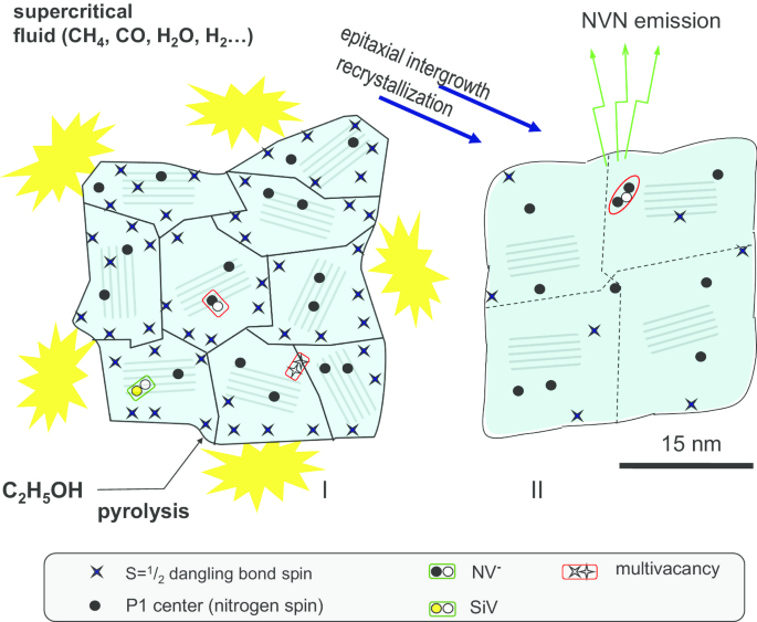
高圧および高温条件での多結晶ダイヤモンド粒子の焼結による、サイズが約30nmのサブミクロンダイヤモンドナノ結晶の概略図。 HPHT焼結(II)後の多結晶(I)とナノ結晶の両方でさまざまな欠陥と色の中心が観察されます
メソッド
サンプルの作成
サブミクロンのダイヤモンド結晶は、平均サイズが25 nmの市販の前駆体多結晶ナノダイヤモンド(製品DP 0〜0.05、Microdiamant、スイス)を焼結することによって調製されました。前駆体粒子は、衝撃波によって誘発されるグラファイトからダイヤモンドへの迅速な変換が発生する爆発支援技術によって得られます( T で100マイクロ秒以内) ≈950°C、 P ≈50GPa)。爆発から生じた生成物は、その後、化学的に処理されてダイヤモンドナノ粒子相を精製し、残留金属とアモルファスカーボンを除去します。粉末は、サイズ>10mμの大きな多結晶で構成されていました。これらの多結晶は、前述の方法[19]に従って、粒界に沿って粉砕および分解することにより、簡単に分別することができます。サイズ分画は、DP 0〜0.05多結晶を形成する小さなサイズの画分を抽出するために行われました。結果として得られる最小の割合のサイズ分布(図2)は、27 nmで最大になり、半値全幅(FWHM)≈25nm(粒子の95%が3〜50 nmの範囲のサイズ)になります。次に、選択された前駆体粒子は、焼結のためにトロイダルタイプの高圧チャンバーの内側のグラファイトシリンダーに移されます。高圧チャンバーの内部の典型的なサイズ(つまり、2つのグラファイトキャップを備えた上記の中空グラファイトシリンダー)は、内径4.0 mm、高さ5.5mmでした。焼結する前に、粒子間スペースが完全に満たされるまで(約30〜50 wt%)、エタノールを乾燥ナノダイヤモンド粉末に滴下しました[18]。次に、高圧(7 GPa)および高温条件(1300±50°C)で10秒間焼結を行いました。ワンプレスの実行中に、約120mgの前駆体ダイヤモンド粉末を処理できました。高圧チャンバーのスキームは、参考文献に記載されています。 [11]。
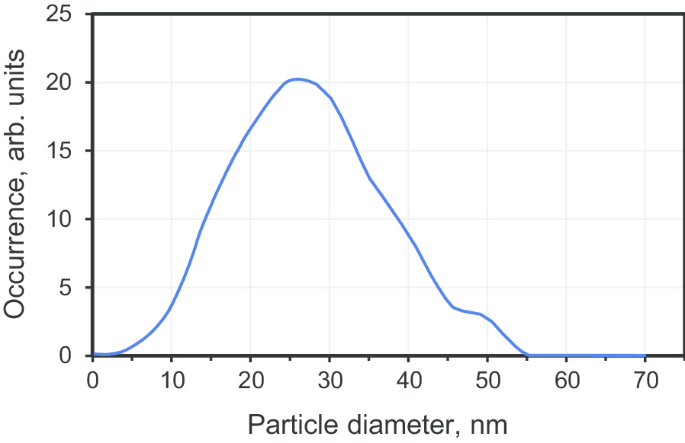
示差遠心沈降装置(CPSディスク遠心分離機、CPS Instruments Inc.、米国)によって測定された平均サイズ〜27nmのDP0–0.05多結晶ダイヤモンドフラクションのサイズ分布
この焼結プロセスの効果を図1に示します。HPHT条件下で焼結すると、エタノールは超臨界状態になります。したがって、多結晶粒界に容易に浸透し、ダイヤモンドの再結晶と新しいダイヤモンド相の成長を促進します。焼結後、〜90–100 mgの許容可能な品質のホワイトダイヤモンド粉末(グラファイト容器からの汚染なし)が高圧チャンバー(ここではD19と表示)から抽出されました。前駆体の灰色/黒色から焼結後の白色への粉末の色の変化は、多結晶の表面の変化とそれに対応する成長を示しています[11]。
焼結前後の材料の構造特性
多結晶ナノダイヤモンド前駆体の構造特性
最初に、焼結前にDP 0〜0.05の構造を特徴づけました。 X線回折(XRD)測定は、CuKα放射線(λ)を使用して、Rigaku Smart Lab IIIX線回折計で行われました。 =1.54178Å)。 40 kVの電圧、30 mAの電流、0.1度/分のスキャン速度を使用しました。 2 θのDP0〜0.05のXRDパターンを図3(黒)に示します。 6°から155°の範囲で。 6つのピークが観察され、そのうち5つ(111、220、311、400、および331)は炭素のダイヤモンド相に特徴的です。観測された最も強いピークは、立方体のダイヤモンド(D c )2 θで111 ≈43.7°。このピークは対称ではなく、左肩を示しています。パターンを2つのローレンツでフィッティングすると、2 θを中心とする最初のピークが生成されます。 =43.76°と2 θで1秒 =41.64°。最初のピークは(111)ダイヤモンド面からの反射に対応し、2番目のピーク(D H とラベル付けされています) 011)は、暫定的に次のいずれかに起因します。(a)六角形の6Hポリタイプダイヤモンド相の平面からの反射[20]、または(b)高応力下での結晶子間の複数の積層欠陥、双晶、および関連する粒界。 D H の積分を比較することによって 011およびD c 111のピーク、DP 0–0.05前駆体の未確認の「相」(六角形または構造欠陥で構成される)は、≈20wt%を表すと推定されます。 002グラファイトとラベル付けされたピーク(2 θ) ≈26°)は、ナノグラファイト相に起因します。この不純物相は簡単に除去できますが、この研究では意図的に酸でエッチングしませんでした。 002ピークと111ピークの面積を比較することにより、このアモルファス相は〜4 wt%に寄与すると評価されました。次に、コヒーレント散乱領域の長さ( L )を評価しました。 CSR )Schererメソッドを使用します。 FWHM βを検討しました 秒θの関数としての5つのダイヤモンドピークの 。 Β は、回折計の応答関数からのデコンボリューション後に決定されます。 脚注1 L CSR DP 0〜0.05のサンプルでは、6.7nmであることがわかりました。
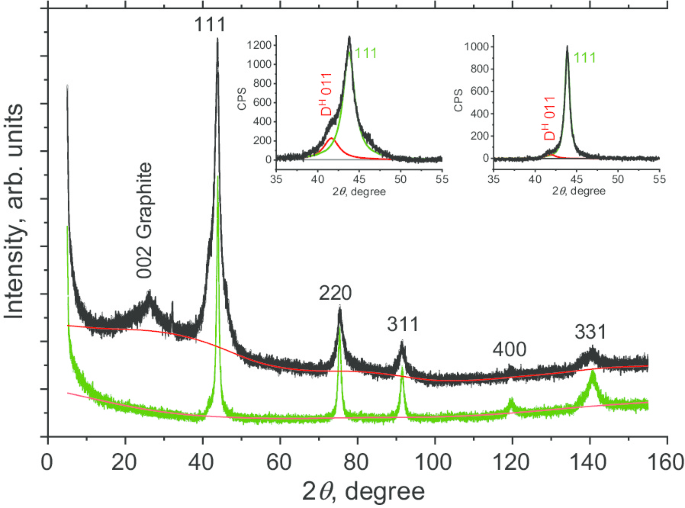
多結晶ダイヤモンド粒子のDP0〜0.05フラクション(黒の曲線)および焼結によって得られたD19ナノダイヤモンド(緑の曲線)の粉末XRDプロファイル。挿入図:41.5°(D H )を中心とする2つの(赤と緑の)ローレンツ曲線を使用した平面(111)からの最も強い反射のフィッティング 011)および43.8 o (D c 111)焼結前(左の挿入図)と焼結後(右の挿入図)のサンプルの場合
複雑な前駆体DP0–0.05ダイヤモンド多結晶構造についてさらに洞察を得るために、高分解能透過型電子顕微鏡(HRTEM、CEOSC補正装置を備えたJEOLJEM-2100F、信州大学)を使用しました。 HRTEMは、照射による損傷を最小限に抑えるために80kVで動作しました。 HRTEM画像(図4)は、多結晶が、特徴的な1.93Å d の緊密に結合した立方体のナノダイヤモンド微結晶で構成されていることを示しています。 -間隔のフリンジ。図4aに示されている多結晶は、5〜12 nmのサイズの結晶子で構成されており、さまざまな色でマークされたさまざまな方向を持っています。さらに、HRTEMは、DP 0〜0.05粉末を構成する個々の多結晶のサイズが、5〜50nmの範囲で広く分布していることを示しています。 HRTEM画像では、六角形のダイヤモンドナノフェーズ(ロンズデーライトなど)の痕跡は見られませんでした。ただし、多くの短い双晶境界が観察され(図4c、d)、それらのいくつかは、図4dのようにアコーディオン形状のプリーツ格子面を示しています。これらの観察結果は、前述の111 XRDピークショルダー(図3)は、六角形のダイヤモンド相の存在ではなく、複数の双晶関連の粒界に関連する積層欠陥が原因である可能性が最も高いことを示しています[16]。
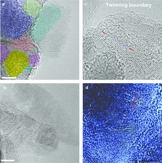
DP 0〜0.05粉末から抽出された選択された立方晶ダイヤモンド多結晶の高分解能TEM画像( a 、 b )およびサンプルで時折見られる長さ数ナノメートルの単純な双晶境界の典型的な画像( c 、 d )。パネル( a 、 b ):スケールバー-4nm。 ( a では、さまざまな結晶子がさまざまな色で強調表示されます )。パネルの矢印( c )および( d )選択した明確に区別できる双子の境界をマークします
DP 0–0.05の元素組成は、有機元素分析システム(JM10、J-Science Lab Co.、Ltd、京都、日本)を使用してPregl–Dumas法で分析しました。このシステムでは、サンプルを1007°Cで酸素流量(30 ml /分)。酸素分率は天秤によって決定された。分析結果(wt%)は、C-90.45、N-2.47、H-0.76、O-6.32です。窒素の濃度が比較的高いということは、ほとんどすべての窒素が、おそらくAセンター(NNダイマー)の形で、凝集した形で多結晶の内部に存在することを意味します。 X線蛍光によるさらなる分析では、DP 0〜0.05に他の微量元素の存在が示されました:Fe(〜300 ppm)、Cu(35 ppm)、Si(120 ppm)、Cr(〜150 ppm)、Ca(〜45 ppm)、Mn(45 ppm)、P(30 ppm)、Al(18 ppm)、Ti(13 ppm)、Mg(6 ppm)、Ni(2 ppm)、Zn(2 ppm)、Co(1 ppm) 。
その後の磁気共鳴研究に使用されるDP0–0.05サンプルは、強磁性金属(主に鉄とクロム)の存在を〜10 ppmレベルまで減らすために、沸騰塩酸でさらに処理されました。
焼結ダイヤモンドの構造特性
また、DP 0〜0.05を焼結して得られたサンプルD19の特性も同様に示しました。 D19 XRDパターンは、DP 0〜0.05粉末の場合と同じ方法で得られました。 111、220、311、400、および331平面に対応する、立方晶ダイヤモンド相に特徴的な5つのローレンツピーク(図3、緑色の線)のみが表示されることがわかりました。前駆体材料にグラファイト相が存在するという証拠はありません。 111ピークの非対称性も大幅に減少します(図3、右挿入図)。これは、スタッキング障害の対応する大幅な削減を示唆しています。さらに、 L CSR コヒーレンス長は10.8nmであることがわかり、焼結中のダイヤモンドナノクリスタライトの拡大を示しています。これらの観察結果を考慮して、我々は、グラファイトおよび非立方晶のダイヤモンド相が、焼結プロセス中に立方晶のダイヤモンド相に変換されると仮定します。これはおそらく、これらの相の溶解と、それに続く多結晶の微結晶間の格子間空間内での立方晶ダイヤモンド相の成長に起因します。このようなプロセスは、デトネーションナノダイヤモンドで以前に観察されています[14]。
D19サンプルの光学および走査型電子顕微鏡画像をそれぞれ図5a、bに示します。ここでは、〜0.3から〜5ミクロンのサイズの任意の形状の粒子が見られます。それらは実際には、共有結合または弱いファンデルワールス結合によって結合された、はるかに小さいダイヤモンド微結晶の高密度のサブミクロンおよび非常に緩いミクロンサイズの凝集体です。このような結合は通常、隣接するダイヤモンド粒子の表面官能基の相互作用から生じます。これらの緩い凝集体を構成する個々のダイヤモンド粒子は、透過型電子顕微鏡で見ることができます。サイズが約〜100nmのD19ダイヤモンド微結晶のTEM画像を図5cに示します。この画像は、JEOL JEM-2100F透過型電子顕微鏡(法政大学)を使用して、加速電圧200kVで撮影されました。サンプルは、カーボン基板なしで銅グリッドに固定されました。
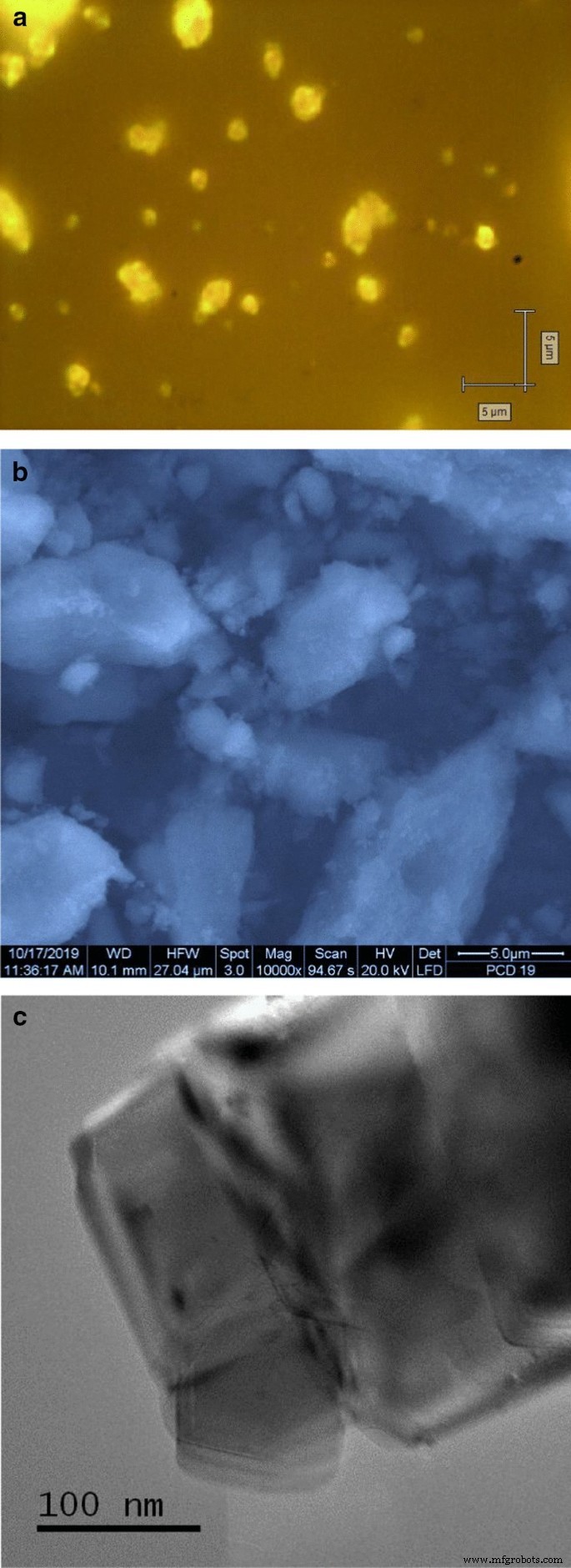
オプティカル( a )、走査型電子顕微鏡( b )、および透過型電子顕微鏡( c )合成されたままのD19ダイヤモンド粒子の画像。光学画像は100倍の顕微鏡対物レンズで撮影されました。電子SEM画像の撮影に使用される対応するパラメータは、パネルの下部に示されています( b )
焼結前および焼結後のナノダイヤモンドの欠陥の含有量を分析する方法
両方のダイヤモンドサンプルは、EPR、ラマン、および蛍光分光法によって分析されました。 EPRスペクトルは、EPR分光計(JES-FA 300、JEOL、日本)を使用して、室温、マイクロ波周波数9.444GHzで記録されました。直径4mmの石英EPRチューブに、20mgの粉末を入れました。チューブ内の粉末カラムの高さは10mmを超えませんでした。チューブの開放端は湿気に対して密閉されていました。
g のEPRスペクトル - g の範囲の係数 =4.00–4.30は P のマイクロ波パワーで記録されました MW =10 mW、磁場変調振幅 A m =1mTおよび周波数ν =100 kHz、アンプゲイン G ≈10 3 、および N =16信号蓄積サイクル。これらのパラメータは、最適な信号対雑音比を得るために選択されました。時定数は0.03秒で、130〜200mTの間隔での磁場掃引の合計記録時間は120秒でした。 g のEPRスペクトル -ファクター g P のマイクロ波電力で、327〜347mTの間隔で≈2が記録されました。 MW =0.03 mW、磁場変調振幅 A m =0.035 mT、アンプゲイン G ≈10 2 、および N =4信号蓄積サイクル。原則として、幅広いメインEPR信号( g ≈2)線幅> 0.5 mT、ピークツーピークEPR信号強度( I pp )MW電力依存性に従います I pp 〜( P MW ) 1/2 P まで MW ≈100mW。一方、狭いEPR信号(低電力で線幅<0.15 mT)の場合、 I pp P で飽和します MW > 0.05mWであり、高い値(> 4mW)で強い形状歪みがあります。このような飽和傾向は、多結晶前駆体とそれに続く焼結ダイヤモンドの両方で観察されました。
マイクロラマン分光計(「inVia」、レニショー、英国)と、50倍の対物レンズ(NA =0.78)およびCCDを使用した光学顕微鏡(ライカ、ドイツ)を使用して、光ルミネセンス(PL)およびラマンスペクトルを取得しました。後方散乱ジオメトリで、検出器を-70°Cに冷却しました。スペクトルは、〜2 cm –1 のスペクトル分解能で記録されました。 。 20 W cm -2 未満の強度で、波長488nmと457nmのアルゴンイオンレーザーの2本のレーザーラインを使用しました。 サンプルの焦点で。ミクロンサイズの円に焦点を合わせる標準と比較して、2×30mμのストライプに焦点を合わせるため、サンプル平面でより低い励起レーザー強度を使用するStreamLine™Plus(レニショー、英国)モードでスペクトル画像を記録しました。この戦略は、周囲雰囲気での過熱と酸化によるレーザー誘起サンプル損傷と局所気相エッチングを制限しました。この手法の詳細と、直径2mmのシリンダーでのダイヤモンド粉末のプレスについては以前に説明されています[19]。
単離されたD19粒子の蛍光画像は、100倍の対物レンズを備えた共焦点広視野落射蛍光顕微鏡で得られました。粒子は、スピンコーティングを介して、D19粉末の希釈された水ベースの懸濁液の上清画分からガラスカバースリップ上に堆積されました。カバースリップは、残留有機物からの寄生蛍光を回避し、D19粒子のカバーガラスへのより良い付着を促進するために、酸素プラズマで事前に処理されました。蛍光は488nmレーザー(励起パワー≈40mW)で励起され、525/40干渉フィルターで収集されました。特別に冷却された2DアレイCCD検出器(カメラ温度=− 79.9°C)を使用して画像を記録しました。画像(サイズ〜80×80μm、80.00 nm /ピクセル)は、60ミリ秒の露光時間で記録されました。画像の表示にはグレースケールパレットを使用しました。画像はFijiソフトウェアを使用して分析されました。
結果
焼結前後の多結晶とダイヤモンド微結晶のEPR
半磁場範囲と高磁場範囲の両方でのDP0〜0.05多結晶ダイヤモンド粉末のEPRスペクトルを図6に示します。これらの異なる範囲で登録されたEPRスペクトルは、高マイクロ波と低マイクロ波で測定されました。パワー P MW =10mWおよび P MW それぞれ=0.03mW。ここで、高磁場領域は通常、主なマイクロ波誘起フリップフロップΔ M に関連する吸収線の近くで選択されました。 s =1スピンの遷移 S =½、一方、拡張されたハーフフィールド範囲は、Δ M からの信号を検索するために特別に選択されました。 s =可能なトリプレット S の2つの遷移 =1センター。ハーフフィールドEPRスペクトルの強度は非常に低く、トリプレットNV - の存在を示しています。 センター( g の信号 =4.27 at H res =158mT [10、16])および三重項多重空孔( g の信号 = H で4.00 res =168 mT [16])多結晶ダイヤモンド前駆体。これらの欠陥タイプは両方とも非常に低い濃度(<1 ppm)で存在します。したがって、そのようなまれな中心を検出するために高いマイクロ波電力を使用する必要がありました。さらに、高磁場領域では、スピンハーフセンター( g )の特徴的な特徴も観察されました。 =2.0027 at H res =337mT [10、16、21])、ただし幅が広い(Δ H pp =0.47 mT)、微細構造のない単一のローレンツ微分形状[16]。これらのスピンが独立した中心からのものであるという仮定を考えると、この広くて強い信号は、暫定的にC–Cダングリングボンドスピンと、結合した常磁性窒素スピンを未解決の超微細構造(HFS)と交換することに起因する可能性があります。 脚注2 スピン S を持つすべての常磁性種の濃度を推定しました =1/2は〜4×10 19 スピン/ g(800 ppm)。これは、5nmのデトネーションナノダイヤモンドについて以前に報告された値の1.5分の1です[22]。
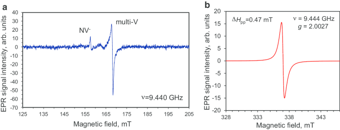
半磁場範囲( a )でのダイヤモンド粒子のDP 0〜0.05フラクションのEPRスペクトル )および g で強い信号を持つ一重項の共鳴磁場の周り -ファクター g ≈2.0027( b )。マイクロ波パワー P MW :10 mW( a )および0.03 mW( b )。マイクロ波周波数ν =9.44GHz。両方のスペクトルは、飽和から遠く離れた領域に登録されています
図7aは、非常に低い( P )のD19サンプルのEPRスペクトルを示しています。 MW =1μW)および非常に高い(200 mW)マイクロ波電力、つまり それぞれ、飽和をはるかに下回るレジームまたは飽和状態(拡大によって証明される)で。 P のスペクトル MW =1Wμには、前駆体粒子の線幅と比較して0.14mTの狭い線幅の中心線があります。図7b(曲線1)は、二重に統合された低マイクロ波電力EPR信号を示しています。この信号は、次のように分解できます。最も豊富な S に関連付けられた幅広い(FWHM≈1.7mT)ローレンツ型信号(図7b、曲線2) =1/2種(局所密度が高く、スピンクラスターに編成されている)および〜6 mTで分離された2つの対称衛星線を持つ非常に狭い中心線(図7b、曲線3)。中心線に対する2つの衛星線の積分強度の比率は、それぞれ0.90と1.09です。したがって、それらは±10%の実験測定精度内で等しい積分強度を持っています。衛星線は、中性常磁性置換窒素のEPR信号の超微細構造に関連しています( 14 N、 S =1/2、 I =1)、P1センターとして知られています[23、24]。 P1中心は、前駆体の多結晶ナノダイヤモンドでは観察されませんでしたが、焼結後のダイヤモンドで明確に検出されました。以前の研究では、P1中心に関連するこの特徴的なトリプレットHFS構造は、サイズが50〜80nmを超える粗いダイヤモンド結晶にのみ現れることが示されています[25]。さらに、エタノールの存在下でのデトネーションナノダイヤモンドの焼結は、ダイヤモンドの再結晶と新しいダイヤモンド相の成長に基づいて結晶子の拡大を促進することが実証されています[26]。したがって、現在のEPRデータは、サイズが〜7–10 nmの多結晶粒子の個々の結晶子から個々のサイズ〜40–50nmの新しい結晶子までここで起こっている同様の拡大と一致しています。 脚注3
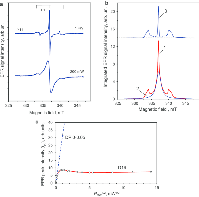
低および高マイクロ波パワーでのD19ダイヤモンド結晶の主な一次微分EPR信号( a )、統合されたEPR信号を2つのグループのスピンに関連するコンポーネントに分解します( b )、および最大200 mW( c )の範囲でのマイクロ波パワーの平方根に対するこのEPR信号のピーク強度の対応する飽和傾向 )。 P1センター(置換窒素)のEPRシグナルのトリプレットHFS構造は、( a )で明確に区別できます。 )。 In( b ):三重項構造を持つ曲線3は、P1中心のみのEPRスペクトルに対応します。 In( c ):破線の直線は I pp vs( P MW ) 1/2 参考のために与えられたDP0–0.05多結晶の依存性。 P での4つの実験ポイント MW =0.5、1、2、4 mWがプロットに使用されました(そのうちの2つはここでは示されていません)。マイクロ波周波数ν =9.44 GHz
この仮説は、狭いEPR信号の観察だけでなく 脚注4 によって確認されます。 ( g =2.0024)HFS特性を持つP1センターの[26]だけでなく、 I の検出による pp P を超える飽和 MW =D19サンプルの場合は0.7mW。前駆体の多結晶ナノダイヤモンドDP0〜0.05の場合、メインEPR信号のピーク強度は、高レベルのマイクロ波パワー( P )でも飽和しません。 MW =20mW)。電力依存性 I pp 〜( P MW ) 1/2 マイクロ波電力の全範囲( P MW =0–20 mW)。 私 pp 〜( P MW ) 1/2 DP 0〜0.05サンプルの依存性は、図7cに破線で示されています。最大〜16mWのマイクロ波電力です。飽和のないこのような線形依存性は、多結晶ナノダイヤモンド内の常磁性中心の高濃度と、非常に短いスピン-格子およびスピン-スピン緩和時間に起因します。 D19サンプルの飽和挙動 g =2.0024EPR信号も図7cに0〜200mWの範囲で表示されます。 脚注5 I を観察します pp 〜( P MW ) 1/2 〜15Wμ未満のマイクロ波電力のみに依存します。この場合、 I pp 1 mW未満の範囲で飽和を示し、〜1mWで最大に達します。 私 pp その後、1〜25 mWの範囲で大幅に減少してから、使用される最大電力(200 mW)までゆっくりと再び増加します。 I におけるそのような飽和傾向の存在 pp ( P MW )、および P の上のドロップも MW =1 mWは、他の欠陥や粒子のエッジから遠く離れた場所にある、スピン-スピンおよびスピン-格子緩和時間が比較的長いP1中心の特徴です[27]。これらの条件は、サイズが60〜80nmを超えるタイプIbHPHTナノダイヤモンドのP1中心濃度が200ppm未満の場合に満たされます。ただし、EPRのみの観点から見た、個々のD19ダイヤモンド微結晶(素粒子)の実際の平均サイズは、未解決の問題です。これは、D19の実際のEPRスペクトルを、平均サイズが18〜390nmの範囲で変化する粉砕されたIbHPHTダイヤモンドの一連の粉末EPRスペクトルと比較することで大まかに解決できます[28]。次の参考文献。 [28]、これらのEPRスペクトルが公開された場合、置換窒素に関連するP1 HFSシグネチャは、平均サイズが30 nm以下の粉末ダイヤモンドには完全に存在しませんが、中間サイズ(85〜130 nm)のサンプルにはまだ存在します。この比較は、合成されたD19ダイヤモンド微結晶の平均サイズが10,030±nmの範囲にあることを示しています。 This estimation coincides well with the representative size observed in the TEM image shown in Fig. 5c. It is notable that the EPR spectrum of D19 recorded at the high power of P MW = 200 mW (Fig. 7a) shows a lack of definition of the HFS structure of the P1 signal. The broad central line suggests the presence, at the nanoscale, of dense clusters of paramagnetic spin-half that strongly couple to each other.
Altogether, the decrease in the linewidth of the main EPR signal (g = 2.0024), the appearance of well-defined HFS characteristics in the P1 centre spectrum after sintering, and the I pp saturation for P MW > 0.7 mW (Fig. 7c) are suggestive of an increase in size by up to one order of magnitude (crystal size > 50 nm). It also indicates a better crystallinity of the nanodiamond in the D19 sample. From van Wyk measurements [29], a smaller amount of paramagnetic defects (< 200 ppm) are expected, based on the narrow linewidth (0.14 mT) of the g = 2.0024 main paramagnetic signal in the D19 sample.
Fluorescence and Raman Scattering of Diamond Crystals
The photoluminescence (PL) spectrum of the DP 0–0.05 precursor together with the PL spectra of some much coarser fractions of polycrystalline diamond particles (DP 0–0.2 and DP 0–0.35) produced by Microdiamant TM is shown in Fig. 8. The spectrum of DP 0–0.05 under the 488 nm excitation wavelength has two features of note:the prominent narrow PL line at 738 nm, associated with the zero-phonon line of negatively charged SiV − centres, and a broad spectrum background with PL bands centred at 525, 600, 660 and 740 nm, associated with various light-emitting centres in diamond, including NV centres. For polycrystals with mean size 25 nm (DP 0–0.05), the intensities of these bands are smaller than that for polycrystals with mean sizes of 100 and 175 nm (DP 0–0.2 and DP 0–0.35, respectively). A more detailed analysis of the PL spectra of polycrystalline DP 0–0.05 particles has been previously undertaken [19].

PL spectra of various submicron fractions of Microdiamant™ polycrystalline diamond particles:blue—DP 0–0.05 (mean size 25 nm), green—DP 0–0.2 (mean size 100 nm), red—DP 0–0.35 (mean size 175 nm). Excitation wavelength λ = 488 nm. The prominent peak at 738 nm marked by the vertical dashed line is the zero-phonon line of negatively charged SiV − centres, which can be observed in all polycrystalline diamond fractions. For better comparison, the spectra are specially normalized for PL intensity at λ = 590 nm. Normalising coefficients are indicated in the figure
Figure 9a shows the PL spectrum of sintered diamond sample D19 (blue curve) at room temperature (RT) together with the PL spectrum of the DP 0–0.05 precursor (red curve). The D19 spectrum displays a green fluorescence characteristic, with a sharp maximum at 525 nm, and a subsequent decrease at larger wavelengths. Note that the single-phonon, sharp Raman line of diamond, which is expected at 522 nm, was too weak to be detected on the ascending slope of the PL signal under 488 nm excitation wavelength. Footnote 6 As previously reported [9, 30], such spectra—with a continuous higher wavelength band of “triangular” shape—are characteristic of optical emission from NVN centres (also known as H3 centres) in submicron (< 140 nm) diamonds at RT. In the PL spectrum of sample D19, at least four broad bands (“bumps”) centred at 538, 569, 601 and 710 nm can be additionally distinguished. We do not believe that they are related to phonon sidebands of the NVN (H3) centres. The origin of the 525 nm sharp peak and “bumps” is still unclear, but it is probably due to an impurity-related complex; the precursor material contains a large number of residual contaminants as mentioned before (see “Structural Characterisation of the Materials Before and After the Sintering” section), some of which are present at significant concentrations (~ 100 ppm). The zero-phonon emission line of NVN at ~ 503 nm wavelength is barely detectable and cannot be distinguished from the two small shoulders (at 500 and 505 nm) in the same region. By comparing the D19 and DP 0–0.05 spectra (Fig. 9a), one can see that they superimpose well for λ > 750 nm. However, the spectra differ significantly in the 480–650 nm range due to the appearance after sintering of NVN centres, which were not present in the precursor material. In order to verify our interpretation of the main optical emission of D19 (in the range 500–650 nm) as originating from NVN centres, we compared the PL spectrum of D19 with the PL spectra of two reference samples (HPHT diamonds, Columbus NanoWorks Inc., US) of two very different sizes and both known to contain NVNs (Fig. 9b). The D19 PL spectrum (dashed line) coincides very well with those of the PL spectra of the HPHT microdiamonds containing NVNs. The emission spectrum of the 100-µm sized reference sample shows a sharp single-phonon diamond Raman line (487.4 nm) and the zero-phonon line (504 nm) of NVN under 457 nm laser excitation at room temperature (Fig. 9b, violet spectrum). The 150-nm sized HPHT nanodiamonds were excited at 488 nm, and it displayed a very similar global photoluminescence spectrum shape as that of the 100-µm sized sample, with a Raman single-phonon line at 522 nm. However, it did not exhibit the NVN zero-phonon line, behaving in that sense exactly like the D19 sample. The “bumps” present in the D19 sample spectrum are absent from both reference PL spectra, indicating that these features are not related to the NVN emission.

PL spectrum of submicron powder D19 sample at T = 293 K (blue line) compared with that of its DP 0–0.05 polycrystalline precursor (red line) under the same conditions with laser excitation at λ = 488 nm (a ), emission spectra, under 457 nm and 488 nm excitation, of two reference synthetic HPHT samples (size ~ 100 μm and < 150 nm) containing NVN centres (b ) and the Raman spectrum of D19 sample recorded using the 457 nm excitation laser radiation (c )。 Arrows in (b ):lines at 487.4 nm and 522 nm are single-phonon diamond Raman lines at 457 nm and 488 nm excitation, respectively, and the line at 504 nm is the ZPL of the NVN centres. In (b):dashed line—PL spectrum of D19 at λ = 488 nm excitation (for comparison). In (c ):the diamond Raman line is centred at 1331.4 cm −1 。 δ = 7.3 cm −1 is a FWHM of diamond Raman line having the Lorentzian shape
We also measured Raman scattering from D19, in the range 1000–1600 cm −1 , under excitation by 457 nm laser radiation. Figure 9c displays the Raman spectrum, corrected to remove the autofluorescence background. The spectrum consists primarily of a narrow characteristic diamond Raman line centred at 1331.4 cm −1 and an exceptionally broad (width ≈ 100 cm −1 ) band centred at 1450 cm −1 。 The latter could be due to non-diamond amorphous carbon phase and/or some transpolyacetylene (TPA) species located at diamond crystals surface [1,2,3]. A further, ill-defined, band at ~ 1090 cm −1 of lower intensity is probably related to TPA species. The broad band at ~ 1450–1480 cm −1 could also be related to multivacancy chains in the diamond lattice and sp 2 - rehybridisation within these chains [6]. Footnote 7 Furthermore, we did not observe the characteristic G-band (centred at 1570–1590 cm −1 ) associated with an sp 2 graphitic nanophase. These observations are indicative that the diamond sample D19 being graphite free, which is also in agreement with its white colour under daylight illumination.
Moreover, the width of the Raman diamond line (7.3 cm −1 ) in the D19 sample is smaller than that for the DP 0–0.05 polycrystalline particles (10.6 cm −1 )。 Table 1 contains Raman diamond line data for bead-milled synthetic Ib HPHT diamonds with mean size varying from 25 to 1000 nm (Microdiamant AG, Switzerland). The linewidth decreases from 9.12 to 5.24 cm −1 with increasing size. This can be explained by the lower prevalence of structural defects in larger crystals. Using data as a calibration curve to infer the crystal size from the diamond Raman linewidth of δ ≈ 7.3 cm −1 yields an estimation for the D19 crystal size of ~ 80 nm. This value coincides reasonably with the estimation in “EPR of Polycrystals and Diamond Crystallites Before and After the Sintering” section on the basis of EPR data. Moreover, this value is very similar to our previous published results where diamonds were obtained by HPHT sintering of 5-nm DND in the presence of ethanol [31]. However, the precursor material used for sintered DND and the one used in this work using the smallest (~ 25 nm) fraction of milled Du Pont shock-wave polycrystalline diamonds are considerably different from the viewpoint of crystal types and elementary crystallite sizes. This obtained size is about 8 times larger than the coherent scattering region length of L CSR ≈ 11 nm extracted from XRD earlier, but it is consistent with crystallite having a low density of structural defects, in agreement with the EPR studies.
<図>We also studied the fluorescence from very fine individual D19 particles. For this purpose, the supernatant fraction of diluted and ultrasonicated water suspension of D19 particles obtained after centrifugation at 4500 × g for a 30 min was used. Coarse particles and large loose aggregates with size exceeding ~ 0.2–0.3 micron were absent in such supernatant. Fine D19 particles were spin-coated onto a thin glass coverslip from the diluted supernatant of D19 particles. A typical image of fine fluorescent D19 particles is shown in Fig. 10a in greyscale (mono 14-bit images). It consists of many spots with different brightness. Some spots, such as that marked by the yellow circle, have sizes close to the diffraction limit. The intensity profile of this spot has a Gaussian shape in its central core and a FWHM of about 5–6 pixel corresponding to ~ 440 nm (Fig. 10b). Such spots come from at least quarter-micron particles and particles of smaller size. A greater number of brighter spots correspond to the larger reassembled aggregates of D19 particles having more NVN colour centres and hence the overall emission intensity increasing.

Wide-field fluorescent image of isolated D19 particles obtained by confocal epifluorescence microscopy (a ), and the intensity profile of the selected nanoparticle marked by the yellow circle (b )。 Image size: ~ 80 × 80 mμ. One pixel corresponds to 80 nm
Discussion
We showed that under HPHT conditions, and in the presence of ethanol, we can convert polycrystalline diamond particles (composed of tightly cemented nanometre-sized cubic diamond crystallites separated by a non-cubic diamond phase) into larger cubic diamond crystallites. The process probably occurs through recrystallisation of the cubic diamond phase and transformation of non-cubic diamond phases including multiple twin boundaries into diamond. During this process, vacancies appear and can form NVN complexes with nitrogen atom pairs. These complexes have a characteristic photoluminescence in the green. While the EPR spectra of the precursor polycrystalline diamonds show NV − triplet centres, triplet multivacancies, and SiV − centres, none of these were present after the sintering. The disappearance of NV − centres and multivacancies has previously been observed [31] after sintering detonation nanodiamonds at HPHT conditions (P = 7 GPa and T ≥ 1350 °C) with ethanol. Footnote 8 The presence of multivacancies is a characteristic feature of damaged diamond lattices, with defects mainly located in a thin layer of ~ 2 nm at the surface. The absence of the paramagnetic triplet and SiV colour centres is strong evidence that substantial recrystallisation took place, accompanied with the appearance of new defect types (NVN). The saturation trend of the substitutional nitrogen (P1 centre) EPR signal with increasing microwave power indicates long spin–spin and spin–lattice relaxation times. These are signatures of improvement of the quality of diamond crystal lattice after sintering. We can assume that during HPHT sintering, vacancies from empty spaces within or between polycrystals join with A-centres to form the new NVN entities.
結論
Sintering of diamond polycrystals, with size varying from 3 to 50 nm, in the presence of ethanol, lead to the substantial enlargement of elementary diamond nanocrystals and improved their crystalline quality. During this process, SiV − and NV − colour centres present in the precursor nanodiamond disappeared, while the EPR signature of P1 substitutional nitrogen paramagnetic centres appeared. We also observed the green photoluminescence of NVN colour centres. The comparison of the FWHM of diamond Raman line (~ 1332 cm −1 ) of the synthesised selected microcrystals under study with those of a series of reference samples revealed that the mean size of diamond crystals after sintering is approximately 80 nm. The analysis of the EPR spectrum dependence upon microwave power demonstrated the good crystalline quality of the synthesised sintered diamond with a concentration of P1 centres smaller than 200 ppm. Hence, our technique of HPHT sintering is a strong alternative to conventional high-energy particle beam irradiation [9] to form NVN centres in nanodiamond. It can be used to produce purely “green” fluorescing nanodiamonds with no (or very limited) crosstalk with the “red” fluorescing nanodiamonds (containing NV 0 and NV − centres), as required in biolabelling for cathodoluminescence integrated correlation electron-light microscopy [32].
データと資料の可用性
The data underpinning this manuscript is available from the corresponding author on request.
Notes
- 1.
The apparatus response function of the XRD diffractometer was determined from a LaB6 reference sample.
- 2.
One mechanism explaining the lack of HFS in the EPR signal of paramagnetic nitrogen in size < 50 nm diamond nanoparticles is described in detail elsewhere [21]. Alternative mechanisms are also not excluded [33, 34].
- 3.
X-ray diffraction CSR size is ~ 4 times smaller in this case.
- 4.
This narrow EPR signal is slightly asymmetrical and consists of at least two components related to P1 centres and to defects having C–C dangling bond spins S = 1/2. The intensity of the second component represents at least 30% of the intensity of the main peak.
- 5.
Here we assume the sequence of untreated first-derivative experimental EPR spectra measured at different P MW , two of which are shown in Fig. 7a.
- 6.
However, the Raman line was detected at 457 nm excitation.
- 7.
The Raman band centred at ~ 1480 cm −1 was found for HPHT diamonds grown with magnesium-based catalysts [6]. Such diamond crystals may contain SiV and GeV colour centres.
- 8.
Instead of a multivacancy g = 4.00 singlet EPR signal, a new EPR signal with a quintet hyperfine structure related to N⋯N pairs separated by no more than 0.7 nm was observed in this case.
略語
- NV − :
-
Nitrogen vacancy
- NVN:
-
Nitrogen-vacancy-nitrogen
- HPHT:
-
High-pressure, high-temperature
- DND:
-
Detonation nanodiamond
- EPR:
-
Electron paramagnetic resonance
- FWHM:
-
半値全幅
- XRD:
-
X線回折
- LCSR :
-
Coherent scattering region length
- HRTEM:
-
高分解能透過型電子顕微鏡
- PL:
-
フォトルミネッセンス
- MW:
-
Microwave
- HFS:
-
Hyper-fine structure
- RT:
-
室温
ナノマテリアル
- ダイヤモンドターニングとは何ですか?
- 選択的レーザー焼結とは何ですか?
- ダイヤモンド
- 磁気センサー用ナノダイヤモンド
- 正方晶ジルコニアナノ粉末の焼結速度に及ぼす少量のSiO2の影響
- セリウムのダイヤモンドカッティングの分子動力学モデリングとシミュレーション
- 多孔質および中空構造のLiNb3O8アノード材料に向けた熱水支援焼結戦略
- 金属支援化学エッチングによって製造されたAuキャップGaAsナノピラーアレイ
- 熱DCプラズマプロセスによって調製されたSi-SiC複合ナノ粒子を用いたスパークプラズマ焼結SiCの焼結挙動
- 1,3-ジメチル-2-イミダゾリジノンの環境に優しい無極性極性添加剤を使用して製造されたペロブスカイト太陽電池
- ホットプレスされたバイドープn型多結晶SnSeの熱電特性