


別個のグラフェン共振器を備えたシステムにおける2つの切り替え可能なプラズモン誘導透明効果
要約
プラズモン誘導透明度(PIT)効果を実現する一般的なプラズモンシステムは、主に単一の結合経路を1つしか許可しないため、単一のPITのみが存在します。この研究では、2つの切り替え可能なPIT効果を実現するために、誘電体格子を搭載したグラフェン層共振器と結合したグラフェンナノリボン(GNR)で構成される別個のグラフェン共振器ベースのシステムを提案します。共振器の交差方向を設計することにより、提案されたシステムは、異なる共振位置と線幅を特徴とする2つの異なるPIT効果を存在させます。これらの2つのPIT効果は、2つの別個の分極選択的結合経路から生じ、分極方向を変更するだけでPITを一方から他方に切り替えることができます。結合効果を実証するためにパラメトリック研究が実施され、物理メカニズムを説明するために2粒子モデルが適用され、数値結果と理論結果の間に優れた一致が見られます。私たちの提案は、調整可能なデュアルバンドセンサーや完璧な吸収体など、切り替え可能なPITベースのプラズモンデバイスの設計に使用できます。
はじめに
表面プラズモンは、絶縁媒体と導電媒体の間の界面で生成される自由電子の集合的な共鳴モードです[1、2]。入射電磁場をサブ波長範囲で1原子スケールの極限サイズに制限する能力があるため[3]、表面プラズモンは強力な光と物質の相互作用を達成するための最も基本的かつ重要な方法の1つになっています[4]。 。この魅力的な光学現象は、さまざまなタイプのプラズモンシステムで見られ、バイオセンシング[5]、非線形光学[6、7]、吸収体[8,9]などのさまざまな最先端のアプリケーションの開発を容易にします。 、10、11]、および他のプラズモン変調器[12、13、14、15]。これらの重要なアプリケーションを実現する可能性は、プラズモン的に誘発された透明性(PIT)のようないくつかの興味深い現象に起因します。 PITとして知られるプロセスは、近接場結合ファノ干渉の結果であり、システム内の共鳴吸収を排除するため、光スペクトルに顕著なウィンドウが生成されることを特徴としています。過去数年間、このようなコヒーレントなプラズモン相互作用は、プラズモンスイッチング[16]、低速光伝搬[17]とセンシング[18]、光ストレージ[19]などのさまざまなアプリケーションを実現するために使用されてきました。
最近の研究では、原子の厚さまでの極薄金属膜が動的な電気的調整可能性を備えていることが明らかになっていますが[20、21]、これらの新規金属によってサポートされるプラズモンは、金属の比較的大きなオーム損失と放射損失に苦しんでいます[22、23]。このような金属の欠点は、金属に支持されたPITのさらなる開発を制限し、新しいプラズモン材料を見つける必要があります。金属プラズモンとは対照的に、グラフェン(対称的な六角形のハニカム格子に形成された密に構造化された炭素原子の単一原子層)によってサポートされるプラズモンは、静電バイアスによって連続的かつ動的に調整できるだけでなく[24、25]、長い伝播もあります長さ。これにより、新世代の再構築可能なプラズモンデバイスが可能になり、アクティブPITを実現するための理想的なプラットフォームが提供されます[26、27]。純金属[16、28、29、30、31]およびグラフェン[32、33、34、35、36、37、38、39、40、41、42]でPITを達成するために、さまざまな材料と設計が使用されてきました。 、またはそれらのハイブリッド材料ベースの[43,44,45]システムでは、これらのシステムのほとんどは単一のPIT効果しか実現できません。たとえば、PITを実現する一般的な方法の1つは、πを設計することです。 -形のある/似たメタサーフェス[16、28、30、33、37、45]。別の方法は、格子結合システムを構築することです[32、34]。ただし、これらの種類の構造では、偏光に依存するシングルウィンドウPITしか実現できません。これは、これらの構造の特殊な幾何学的非対称性により、すべてのナノ構造共振器が、明るい(放射/超放射)モードまたは暗い(非放射/サブ放射)モードのいずれかとして動作するように事前設定されているためです。したがって、それらは1つの特定の偏光方向で1つの明るいから暗い結合経路のみを許可し、1つの偏光依存PIT効果のみをもたらします。私たちの以前の研究は、純粋なグラフェンナノリボン(GNR)[35]または格子結合[38]構造の2つの明暗モード結合経路を備えたPITシステムを示しましたが、タリー偏光非感受性シングルウィンドウPITまたは偏光依存ダブルこれらのシステムでのウィンドウPIT効果は、幾何学的パラメーターの特定の選択に強く依存します(説明の部分を参照)。
この論文では、2つの別個のPIT効果を結合して実現するために、2つの異なる共振器、つまり誘電体格子を搭載したグラフェンシートと結合するGNRを使用することを提案します。垂直共振方向を設定することにより、両方の共振器で共振する表面プラズモンが、入射光の異なる偏光方向で生成され、2つの異なる偏光依存結合経路、したがって2つの別個のPIT効果が生じることを示します。さらに、パラメトリックスタディを使用して、結合メカニズムを詳細に調査します。そして、高度なシミュレーションと2粒子モデルベースの理論的分析の両方を組み合わせて、これらの切り替え可能なPIT効果を実証します。最後に、屈折率センサーや完全吸収体など、提案されたシステムの潜在的なアプリケーション、および他のPITシステムとの比較について説明します。
デザインとマテリアル
このパートでは、本研究で使用した数値モデルと関連資料を紹介します。私たちのモデルでは、古典電磁気学のみを考慮し、GNRの量子有限サイズ効果、グラフェンの非線形効果、および基板フォノン効果から生じる可能性のある効果を無視すると述べています[46]。提案されたシステムの概略図を図1に示します。2つのグラフェン層が x に配置されています。 o y 平面であり、ドープされたSiまたはSiO 2 によって分離されています 屈折率 n の導体 3 と厚さ d 。最初の層は、 x の周期を持つ下部グラフェンナノリボン(LGNR)によって形成されます。 方向。 2番目の層はグラフェンシート全体であり、屈折率 n の誘電体格子でさらに覆われています。 1 (上部グラフェン格子、UGGとしてラベル付けされています)および周期 P d y 方向。幾何学的パラメータは W として固定されています r = W d =50 nm、 p r = p d =100 nm、 h =100 nm、および d =20 nm、図1で定義されています。グラフェン層を囲む他の材料の誘電率は n に設定されています。 0 および n 2 、図1に示されています。簡単にするため、一般性を失うことなく、誘電率は n と仮定されます。 1 =2.0および n 0 = n 2 = n 3 =1.0。屈折率の虚数部を無視しても、この研究の基本的な結論は変わりません。特に指定がない限り、上記のパラメーターは同じままであることに注意してください。技術的には、設計された2層グラフェンベースのPITシステムの実現は、層状グラフェンシステムの製造に最近使用された十分に開発されたパターニングおよびグレーティング技術を使用して実験的に実現可能です[27、47]。
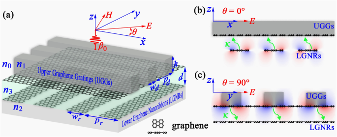
3D( a )および2D側面図( b 、 c )提案されたPITシステムの。周期的な誘電体格子がロードされた1つのグラフェン層は、交差した格子とリボンの方向を持つ周期的なGNRの1つの層の上を覆います。上部グラフェン格子層は、格子幅 W で設計されています d 、高さ h 、および横周期 P d 、下部グラフェンナノリボンのリボン幅は W r および期間 P r 。 2つのグラフェン層間の距離は d です。 、これは導電性のSiまたはSiO 2 で満たされていると想定されます 屈折率 n のスペーサー 3 。誘電体格子およびその上のGNRの屈折率は、 n とラベル付けされています。 1 、 n 0 、および n 2 、 それぞれ。波数βの直線偏波平面波 0 偏光角θ x に関して -軸は通常、層状グラフェンシステムの表面に衝突します
メソッド
提案された構造は、Lumerical FDTD Solutionsに基づく有限差分時間領域(FDTD)法を使用して数値的にシミュレートされます。私たちのシミュレーションでは、周期境界条件がx方向とy方向の両方で使用されています。広帯域平面波はz方向から入射し、それに沿って完全に一致した層が適用され、境界に出てくるすべての光を吸収します。電界分布は、2つの層間のグラフェン表面までの距離が0.5 nmの共振波長で、2D電界プロファイルモニターによって収集されます。その上、グラフェン膜はランダム位相近似(RPA)[48、49]の範囲内で記述されます。この近似の範囲内で、面内光伝導率σ グラフェンのは、σとして中赤外線範囲の半古典的なDrudeのような表現として記述されます。 (ω )= ie 2 E F / [πћ 2 (ω + iτ -1 )] [24、50]。ここで、 E F =ћν F ( n g π ) 1/2 はグラフェンのフェルミ準位で、 n g = (μ/ћν F ) 2 /π キャリア濃度である(ここでμ =15,000 cm 2 /( V × s )は、測定されたDC移動度νです。 F =10 6 m / sはフェルミ速度であり、ћ は縮小プランク定数)であり、電気ゲーティング[24、25、50]、ωによって調整できます。 は角周波数であり、τ=μE F / ( ev F 2 )はキャリア緩和時間です。この論文では、 E F 特に指定がない限り、0.6eVに固定されています。私たちのシミュレーションでは、グラフェンの光学特性は、異方性比誘電率テンソルを使用して記述されています[35]。 z グラフェン誘電率の成分はεとして設定されます zz =2.5はグラファイトの誘電率に基づいていますが、面内成分はεです。 xx =ε yy =2.5 + iσ (ω )/(ε 0 ωt )[24、51]、ε 0 は真空誘電率であり、 t =1nmはグラフェンの厚さです[35]。
x の両方に2粒子モデルを適用する および y 軸については、次の一連の方程式[8、52、53]によって、図1に示す有効なプラズモン共鳴と結合を理論的に分析できます。
$$ {a} _ {1i} ^ {{\ prime \ prime}}(t)+ {\ gamma} _ {1i} {a} _ {1i} ^ {\ prime}(t)+ {\ omega} _ {1i} ^ 2 {a} _ {1i}(t)+ {\ kappa} _ {12i} ^ 2 {a} _ {2i}(t)={Q} _ {1i} E \ sin \ theta / {m} _ {1i} $$(1)$$ {a} _ {2i} ^ {{\ prime \ prime}}(t)+ {\ gamma} _ {2i} {a} _ {2i} ^ {\ prime}(t)+ {\ omega} _ {2i} ^ 2 {a} _ {2i}(t)+ {\ kappa} _ {21i} ^ 2 {a} _ {1i}(t) ={Q} _ {2i} E \ cos \ theta / {m} _ {2i} $$(2)ここで i = x または y ; γ i は損失係数であり、スペクトルの線幅に関連しています。 ω i は共振器の共振周波数です。 Q i モードの実効電荷であり、共振モードの強さを示します。および m i 対応する共鳴配向における粒子の有効質量です。 κ i i の2つの層の間の結合強度です。 方向。これは、2つの結合モードの電子-電子相互作用に対応するため、プラズモンの特殊な場の分布と共振器間の結合距離によって決まります。プラズモン結合が結合強度κの2つの座標軸にのみ沿っていることを考慮すると 12 i =κ 21 i =κ i 、システムを、異なる方向で独立して共振する2つの別個の共振器グループとして扱うことができます。すべての粒子が入射電場 E と結合すると仮定します = E 0 e iωt 、変位ベクトル a を生成します i = c i e iωt 。式でいくつかの代数計算を実行した後。 (1)と(2)では、プラズモンのモード振幅は次のように表すことができます。
$$ {a} _ {1i}(t)=\ frac {\ kappa_i ^ 2 {Q} _ {2i} E \ cos \ theta / {m} _ {2i} + \ left({\ omega} ^ 2 -i {\ omega \ gamma} _ {2i}-{\ omega} _ {2i} ^ 2 \ right){Q} _ {1i} E \ sin \ theta / {m} _ {1i}} {\ kappa_i ^ 4- \ left({\ omega} ^ 2-i {\ omega \ gamma} _ {1i}-{\ omega} _ {1i} ^ 2 \ right)\ left({\ omega} ^ 2-i { \ omega \ gamma} _ {2i}-{\ omega} _ {2i} ^ 2 \ right)} $$(3)$$ {a} _ {2i}(t)=\ frac {\ kappa_i ^ 2 { Q} _ {1i} E \ sin \ theta / {m} _ {1i} + \ left({\ omega} ^ 2-i {\ omega \ gamma} _ {1i}-{\ omega} _ {1i} ^ 2 \ right){Q} _ {2i} E \ cos \ theta / {m} _ {2i}} {\ kappa_i ^ 4- \ left({\ omega} ^ 2-i {\ omega \ gamma} _ {1i}-{\ omega} _ {1i} ^ 2 \ right)\ left({\ omega} ^ 2-i {\ omega \ gamma} _ {2i}-{\ omega} _ {2i} ^ 2 \右)} $$(4)実効電気感受率(χ eff )、これは総分極率( P )間の比率を示します )プラズモン共振器と入射電場の強さの場合、変位ベクトルの形式で次のように表すことができます。
$$ {\ displaystyle \ begin {array} {c} {\ chi} _ {e \ mathrm {ff}、i} =\ frac {P_i ^ 2} {\ varepsilon_0E} =\ frac {Q_ {1i} {a } _ {1i} + {Q} _ {2i} {a} _ {2i}} {\ varepsilon_0E} \\ {} =\ frac {\ left [{\ kappa} _i ^ 2 {Q} _ {1i} {Q} _ {2i} + \ left({\ omega} ^ 2-i {\ omega \ gamma} _ {2i}-{\ omega} _ {2i} ^ 2 \ right){Q} _ {1i} ^ 2 \ right] \ sin \ theta / {m} _ {1i} + \ left [{\ kappa} _i ^ 2 {Q} _ {1i} {Q} _ {2i} + \ left({\ omega} ^ 2-i {\ omega \ gamma} _ {1i}-{\ omega} _ {1i} ^ 2 \ right){Q} _ {2i} ^ 2 \ right] \ cos \ theta / {m} _ { 2i}} {\ varepsilon_0 \ left [{\ kappa} _i ^ 4- \ left({\ omega} ^ 2-i {\ omega \ gamma} _ {1i}-{\ omega} _ {1i} ^ 2 \ right)\ left({\ omega} ^ 2-i {\ omega \ gamma} _ {2i}-{\ omega} _ {2i} ^ 2 \ right)\ right]} \ end {array}} $$( 5)次に、シミュレートされた透過および吸収スペクトルは、磁化率の虚数部に適合させることができます。この論文では、吸収は A として定義されています。 =Im [χ eff、 i ]。この係数は、エネルギー保存の法則 T から導き出されます。 + A =1;したがって、トランスミッション T の表現があります。 =1 − Im [χ eff、 i ]。
結果
PIT効果の励起
PIT効果を励起するために解決する必要がある問題の1つは、ブライトモード共振器をどのように設計するかです。入ってくる自由空間波とプラズモン波の間の大きな運動量の不一致のために、プラズモンの励起は、グラフェンプラズモンの使用に関する主要な課題の1つです。これを終わらせるために、グラフェンプラズモンの励起を可能にするいくつかのアプローチが提案され、理論的および実験的に実証されています。最初に一般的に使用される方法は、グラフェン単分子層をナノリボン[25、54]、ナノディスク[55、56]、円[24]などの共面ナノ構造にパターン化することです。別の方法は、連続グラフェンシートに格子構成を構築することです。これは、回折誘電体格子[51、57]と電界ゲート[58]を使用して位置依存の周期的局所伝導率格子を構築するか、周期的回折格子を使用することによって実現されます。グラフェンシート自体によって形成された波形格子[57、59]。これらのグラフェン構造で表面プラズモンを励起できる理由は、ナノ構造またはグレーティングが、偏光方向が周期方向に沿っている場合の波数ベクトルの不一致の補償に必要な追加の相互波数ベクトルをプラズモン波に提供できるためです[51 、54、59]。この状態では、グラフェン共振器は明るいモードとして動作することも、暗いモードとして機能することもあります。ここでは、図1に示すように、GNRと長方形の誘電体格子を搭載したグラフェンシートの両方を使用して、それぞれ明るいモードと暗いモードとして機能し、PITシステムを構築することを提案します。
提案されたPITシステムのメカニズムを探求するために、図1に示す構成の数値シミュレーションを計算し、2つの異なる偏光角に対応する結果を図2に示します。θ> =0°の場合、最初に、下部グラフェンナノリボン(LGNR)と上部誘電体格子負荷グラフェンが単独で存在する状況の結果を計算しました。分極方向はLGNRに垂直であるため、SPはLGNRで励起され、図2aに示す青い線のように、5.327μmに主な吸収ピークが生じます。対照的に、図2aの平らな緑色の線で示されているように、入射光は誘電体格子に平行に偏光され、強い運動量の不一致が生じるため、上部グラフェンシートのSPはこの偏光条件では励起できません。これらの状況では、図2gおよびfに示すように、LGNRの直接励起モードとUGGのダークモードをそれぞれLGNRs-0およびUGGs-0と呼びます。ただし、ここで興味深いのは、これら2つのグラフェン層が集まって十分に接近すると、5.747μmと4.917μmに2つの吸収ピーク(透過率の低下)が現れることです。図に示すように、共鳴波長が長い方が吸収が47.16%に達することが支配的であるのに対し、共鳴波長が短い方は35.88%の吸収ピークが特徴であり、これら2つのモードが外部入射光と非常に強く相互作用することを示しています。 。2aおよび表1で結論付けられています。これらの2つのモードは、2つの共振器間の同相および逆相のプラズモニック結合に起因します。具体的には、LGNRのブライトモード共振は、入射光によって直接励起されるため、固定モードと見なす必要があります。ただし、上部グラフェン層のプラズモン共鳴は直接励起することはできませんが、同相相互作用と逆相相互作用の両方を介してLGNRで励起されたプラズモン共鳴と結合することができます。このPIT効果を直接もたらすのは、2つの共振器とそれらのプラズモン結合の共存です。 2つのモードの起源の背後にある物理的メカニズムを明確に明らかにするために、図2hおよびiにこれら2つのモードでの電界分布を表示します。 E によると z 成分の電界分布では、5.747μmのモードは層状構造の同相共振の性質を示しているため、対称モードと呼ばれます。 4.917μmのモードは逆位相共振を示し、反対称モードと呼ばれます。さらに、図2hとiは、これらのモードの構造を明確に示しています。すべての E z コンポーネントは、2 πによって特徴づけられる双極子モード共鳴を示します 偏光方向に沿った位相シフト( x 軸)各グラフェン層。これらの2つの基本モードは、LGNRの共鳴吸収を排除すると同時に、光スペクトルに顕著な透過ウィンドウと2つの吸収ピークを生じさせ、PITと呼ばれる光学効果を引き起こします(説明の便宜上、これをLGNR-PITと呼びます)。図2cでは、2つの吸収ピークでの透過位相と遅延時間もプロットしています。後者はそれぞれ0.34psと0.36psに達し、システムでの光の減速効果を示しています。
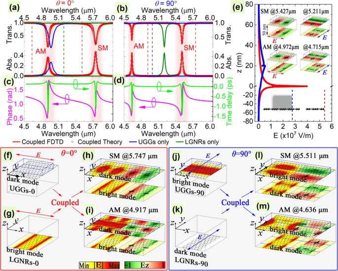
透過線と吸収線( a 、 b )とその送信フェーズ(左 y 軸)と遅延時間(右 y 軸)( c 、 d )偏光角θのシステムの =0°( a 、 c )および90°( b 、 d )、 それぞれ。 In( a )および( b )、破線は他の偏光での共振位置を示しています。 ( a の理論的に分析された線のフィッティングパラメータ )および( b )は(THzで)6.71、110.07、2.25、0.46、および0.74であり、κの場合は5.73、4.13、72.83、0.33、および0.27です。 i 、 Q 1i / sqrt(ε 0 m 1i )、 Q 2i / sqrt(ε 0 m 2i )、γ 1i 、およびγ 2i 、 それぞれ。 UGGの場合の電界の空間分布( e (青い線)、 f 、 j )およびLGNR( e (赤い線)、 g 、k) z に沿ってのみ 軸( e )および対応するグラフェン平面( f 、 g 、 j 、 k )。電界の空間分布(左のパネル)と対応する z 対称モード(SM)のコンポーネント(右側のパネル)( h 、@5.747μm; l 、@5.511μm)および反対称モード(AM)( i 、@4.917μm; m 、@4.636μm)偏光角θ =0°( h 、 i )および90°( l 、 m )、 それぞれ。 e の上部インサート 表示 z d の場合の電界の成分 =50 nm、下の挿入図はメインプロットのフィールドの位置を示しています。記号「+」および「-」は、共鳴する表面電荷を提供します。色が濃いほど電荷密度が高いことを示します
θの場合 =90°、SPは5.202μmに主な吸収ピークを持つUGGで励起できますが、図2bに示す緑と青の線のように、LGNRが単独で存在する場合は励起できません。これらの状況では、図2jおよびkに示すように、UGGの直接励起モードとLGNRのダークモードをそれぞれLGNR-90およびUGG-90と呼びます。ただし、これら2つのモードが互いに結合するのに十分近い場合、2つの透過ディップ(吸収ピーク)が5.511μmと4.636μmに明確に現れ、吸収はそれぞれ49.07%と46.46%に達します。これは、外部入射波との相互作用を意味します。図2bに示され、表1で結論付けられているように、非常に強力です。θの場合と同様です。 =0°の場合、物理メカニズムは、2つのグラフェン層間の同相および逆相のプラズモン結合を考慮することによっても理解できます。図2lとmに明確に示されているように、 E z 成分場の分布は、2 πが特徴の双極子モード共鳴を示しています。 y に沿った位相シフト 各グラフェン層の軸を示し、対応する吸収ピークで同相(対称モード)および逆相(反対称モード)の共鳴を示します。顕著な透過ウィンドウと光スペクトルの2つの吸収ピークを生成しながらUGGのみでケースの共鳴吸収を排除するのはこれらの2つの基本モードであり、別のPITをもたらします(説明の便宜上、これをUGG-PITと呼びます) )。図2dには、2つの吸収ピークでの透過位相と遅延時間もプロットされており、対称モードと反対称モードでそれぞれ0.23psと0.21psのピーク値を持つ低速光伝搬効果を示しています。
ただし、図2iおよびmの非対称モードの上部グラフェンシートの電界分布は「多重極」共鳴の外観を示していますが、電荷振動も次の性質を維持しているため、双極子モードであることに注意してください。偏光方向に沿った双極子モード共鳴。 「多重極」共鳴の外観の理由は、LGNRからの強い場の干渉によるものです。これは、図2eに示すように、パターン化されたGNRの最も強い局在プラズモン場が連続グラフェンシート[60]よりも顕著であるという事実を考慮することで理解できます。これらの「多重極」モードの外観は、2つのグラフェン層からフィールドモニターを設定するか、 d の場合など、大きな結合距離を使用することで消えます。 =50 nmの場合、図2eの挿入図に示すように、「多重極」モードの外観は純粋な双極子モードの共振に変化します。さらに、2つのグラフェン層の間のモード結合が異なることにも注意してください。具体的には、θの場合 =0°、LGNRs-PITは、 x に沿って共振するLGNRs-0とUGGs-0の間の強い結合の結果です。 方向。 θの場合 =90°、UGGs-PITは、 y に沿って共振するUGGs-90とLGNRs-90の間の強い結合の結果です。 したがって、LGNRs-PITとUGGs-PITは、異なる偏波で共振する異なるモード間のプラズモン結合の効果であり、2つの異なるPIT効果をもたらします。
したがって、図2から、LGNR-PIT(θを使用)であると結論付けることができます。 =0°)およびUGGs-PIT(θを使用) =90°)は、層状グラフェンシステムの2つの別々の明るいモードから暗いモードへの結合経路から生じ、異なるスペクトル応答によってチャーターされた2つの異なるPIT効果です。つまり、入射光の偏光方向を変えるだけで、これら2つのPIT効果を一方から他方に切り替えることができます。これは、偏光に影響されないPIT効果とは大きく異なります(説明の部分を参照)。さらに、この切り替え可能なPIT効果は、式(1)に示す2粒子モデルによって説明できます。 (1)と(2)。 θの場合 =0°の場合、式の右辺で示されているように、UGGの入射フィールドへの直接結合効率はゼロ(暗い)ですが、LGNRの直接結合効率は最も高く(明るい)です。 θの場合 =90°、またはその逆の場合、UGGは明るくなりますが、LGNRは暗くなります。どちらの場合も、式(1)で得られた分析結果間の一致に注意してください。 (5)(図2a、bの赤い円で表されている)と数値結果(図2a、bの赤い線でプロットされている)はほぼ完全です。私たちの分析モデルは、図2で明らかなように、位置だけでなく共振のピーク値も非常に正確に予測します。最後に、ここに示す結果は、同じ共振器[35、38];これは、異なる偏光では図2に示す結果が得られないためです。違いについては、ディスカッションパートでさらに説明します。
PITの幾何学的な調整可能性
明るいモードと暗いモードの間の近接場結合が、2つの偏光依存PIT効果をもたらすことを実証しました。したがって、明るいモードと暗いモードの共振、およびそれらの間の結合強度に大きな影響を与えるパラメーターは、PIT効果の調整可能なパラメーターとして扱うことができます。まず、θの場合のパラメトリックスタディを実行します。 =幅を変更して0°( W r )LGNRと幅( W d )20〜100 nmのUGGの結果を、それぞれ図3aとcに示します。 LGNRは入射光と直接結合し、これらの条件で明るいモードとして機能するため、LGNRの寸法の変化は、システムのプラズモン応答全体に直接影響します。たとえば、 W の場合 r が非常に小さく、たとえば20 nmの場合、GNRの占有率が低いために入射光との結合効率が非常に弱く[14、51]、反対称モード、特にPITシステムの対称モードの吸収が低くなります。 W の吸収線からわかるように r =図3aでは20nm。別の例として、 W の場合 r は十分に大きく、特に最大100 nmに達すると(つまり、LGNRがグラフェン層全体である場合)、2つの共振器のいずれも外部電界と結合できないため、LNGR-PITは消えます。特に、2つのモードの吸収は、 W のときに同時に最大値を示します。 r 約50nmです。明るいモードとは異なり、DG幅のバリエーション( W d )ダークモードの上部グラフェン層では、制限内で対称モードと反対称モードの共振位置と吸収を調整することしかできませんが、図に示すように、外部波との高い結合効率を排除することはできず、大きな影響を与えることさえできません。 3c。実際には、誘電体格子が除去されたり、誘電体層全体になったりしても( W d =100 nm)、前の研究[36]で説明されているように、LGNRは上部グラフェンシートと結合できます。この場合、PIT効果は1つしか存在できません。
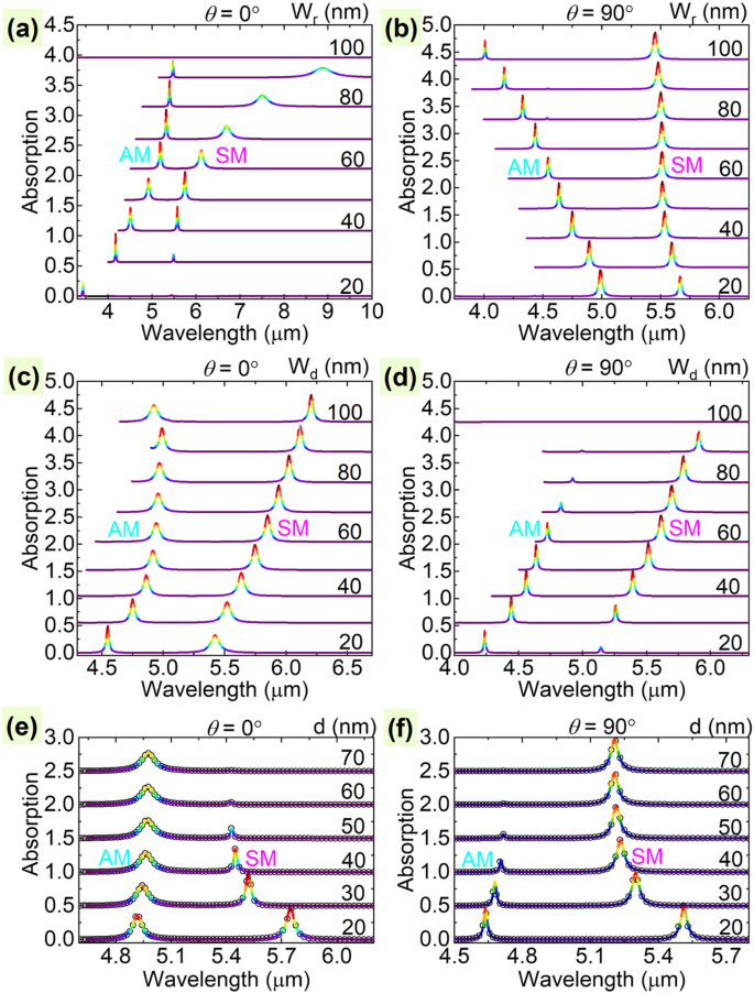
( a の関数としての波長スケールでのPITシステムの吸収スペクトル )、( b )リボン幅 W r LGNRの; ( c 、 d )DG幅 W d UGGの;および( e 、 f )分離距離 d θの偏光角で10 / 20nmのステップで2つのグラフェン層の間 =0°( a 、 c 、 e )および90°( b 、 d 、 f )、 それぞれ。 In( a – f )、実線の濃い赤色は吸収が強いことを示します。他の高次の吸収ピークからの注意散漫を避けるために、一部の線がカットされていることに注意してください。 In( e )および( f )、実線の曲線とくまは、それぞれ数値結果と理論結果を示しています。 SMとAMは、それぞれ対称モードと反対称モードを指します
ただし、θの場合 =90°、結果はθの場合とは対照的です =0°。LGNRはダークモードとして機能し、UGGはブライトモードとして機能するためです。詳細には、LGNR幅の変更 W r 図3bに示すように、対称モードと反対称モードの共振位置と最大吸収を変調するだけで、2つのモードの存在を消滅させることはできません。これは、LGNRがこの偏光状態でダークモードとして動作するためです。 W の状態 r =100 nmの場合、システムはDGをロードしたグラフェンシートが別のグラフェンシートと結合します。これは、別の研究で以前に報告された2次元の単一PITシステムに似ています[34]。ただし、上部のグラフェンシートはこの状態で明るいモードとして機能するため、上部の誘電体格子の変更はPITシステムの光学応答に大きな影響を与えます。これは、 W を変更した場合と非常によく似ています。 r θ =0°、図3dに示すように。一般に、図3a〜dから、明るいモードの調整は、図3aおよびdに示されているように、UGGs-PITの外観、さらには存在に大きく影響すると結論付けることができます。ダークモードは、図3bとcに示すように、UGGs-PITの対称モードと反対称モードの共振位置と相対強度のみを変更できます。
PIT効果に大きく影響するもう1つのパラメーターは、スペース d です。 2つのグラフェン共振器の間。 GNRと誘電体格子の幅を固定してから、 d を増やします。 , the interaction strength between the two graphene resonators decreases monotonically for both polarization angles due to the fast decreasing plasmonic field in the normal direction of the graphene surface [35, 61]. As a result, the symmetric mode and the antisymmetric mode are respectively extinguished for the case with θ =0° and θ =90° at large coupling distance, e.g., d> 70 nm, as shown in Fig. 3e and f. As it is known that when the bright and dark modes are far beyond the decay length of the evanescent field of each other, these two modes are uncoupled, and therefore, only the bright mode exists. At that point, we can conclude from Fig. 3e and f that the symmetric mode and antisymmetric mode of the PIT respectively originate from the UGGs and LGNRs, as they remain at large layer distance. Note that the PIT effects at different coupling strengths match well with the two-particle model, as the simulated and analytically predicted results are in excellent agreement, as can be seen in Fig. 3a and b, where the solid curves are gotten from FDTD, and the dark circles are from the two-particle model.
Electrical Tunability of PIT
One of the major advantages of graphene-based plasmonic devices is their dynamic and broadband tunability, which can be realized by electrostatic gating techniques [61, 62]. This intriguing property allows us to electrically change the Fermi energy of graphene and, thus, to actively modulate the transmission window of the proposed PIT systems to work at different wavelengths without reconstructing the geometrical structure [24, 25]. By applying different bias voltages with a field-effect transistor structure, researchers have experimentally achieved the dynamical tune of the Fermi energy level from 0.2 to 1.2 eV [63]. The simulated absorption spectra shown in Fig. 4 confirms the broadband and dynamic tunability of the proposed PIT device. For the given geometrical parameters, the plasmon wavelengths of the symmetric mode and antisymmetric mode of the LGNRs-PIT (UGGs-PIT) can be tuned from 4.977 to 9.953 μm and 4.259 to 8.520 μm (from 4.775 to 9.551 μm and 4.015 to 8.033 μm) when the Fermi level is modulated from 0.8 to 0.2 eV, respectively, as the solid and dash-dotted lines shown in Fig. 4a and b. This dynamic tunability will greatly facilitate the design and practical application of the proposed PIT device.

Absorption spectra of the symmetric mode (solid lines) and antisymmetric mode (dash-dotted lines) of the proposed PIT system with different Fermi energy levels of graphene at polarization angles of θ =0° (a ) and 90° (b )、それぞれ
Applications
In the previous parts, we have made clear how the LGNRs couple with the UGGs and further result in the polarization-dependent PIT effects, and demonstrated how the geometrical and electrical parameters affect the couplings. In this part, we will demonstrate our proposal can be used as selective refractive index sensors and dual-band perfect absorbers.
Considering that the PIT effect is determined by both the bright and dark mode resonances, what brings the change to these two modes will directly alter the symmetric mode and antisymmetric mode in the PIT window. Therefore, the induced symmetric mode and antisymmetric mode are highly sensitive to the local dielectric environment, which can be applied to design refractive index sensors [64]. In our design, both the regions above the UGGs (with refractive index n 0 ) and below the LGNRs (with refractive index n 2 ) can be thought of as the sensing regions. To calculate the sensitivities, we define S =Δλ/ Δn , which specifies the plasmon wavelength (λ ) shift per refractive index unit (RIU). We assume the refractive indexes of the materials as n 1 =2.0 and n 0 =n 2 =n 3 =1.3 (except the cases when n 0 or n 2 is working as the sensing regions with the range changing from 1.0 to 1.1).
Firstly, when tuning the width of the GNRs (W r ), we find that when the sensing region is alongside the bright mode (that are sensing region n 0 with θ =90° and sensing region n 2 with θ =0°), the sensitivity of the symmetric mode S SM gets bigger at wider ribbon width (see the solid blue lines in Fig. 5b, c). Especially, S SM can reach 4 μm/RIU for the case with θ =0° in sensing region n 2 。 Secondly, for the case with increasing DG width (W d ), both the sensitivity of the symmetric mode S SM and antisymmetric mode S AM decrease in most cases. Finally, as for the coupling distance d between the two layers, it is found that S SM decreases while that of the antisymmetric mode increases for both of the polarization angles (see the solid and dash-dotted dark lines in Fig. 5). Considering that the antisymmetric mode will disappear under large coupling distance at the polarization angle of θ =90° (see Fig. 3f), the antisymmetric mode for the situation with θ =0° is more suitable to work as a sensor at a larger distance. Generally, the sensitivities of the symmetric mode and antisymmetric mode of the LGNRs-PIT and UGGs-PIT are respectively comparable to each other, as can be concluded by comparing Fig. 5a with 5b, and Fig. 5c with 5d, respectively. Besides, it is also found that the sensitivities for the cases with sensing regions alongside the bright and dark modes do not show a big difference, as can be seen by comparing Fig. 5a with 5d (alongside the dark mode), and Fig. 5b with 5c (alongside the bright mode). However, the sensitivities of the case with the sensing region under the LGNRs are obviously higher than that of the case with the sensing region above the UGGs, as they are shown by comparing Fig. 5a and b with Fig. 5c and d. This is because the sensitivity is directly related to the localized plasmonic field [64], and the local plasmonic field in the cutting-edge nanoribbons is generally stronger than the continuous edge-free graphene dielectric gratings [60].

Refractive index sensitivities of the symmetric mode (SSM , solid lines) and antisymmetric mode (SAM , dash-dotted lines) in the sensing regions of n 0 ( a 、 b )および n 2 ( c 、 d ) as functions of the ribbon width W r of LGNRs, the DG width W d of UGGs, and the separation distance d between the two graphene layers at polarization angles of θ =0° (a 、 c ) and 90° (b 、 d )、 それぞれ。 The inserts show the location of the sensing region
Besides working as a refractive index sensor, the proposed system can also be further designed as a perfect absorber. To achieve this, we can add a metallic substrate below the LGNRs and assume the refractive indexes of the materials as n 1 =2.0 and n 0 =n 2 =n 3 =1.3. With the existence of the metallic substrate, the dielectric layer between the LGNRs and metallic mirror forms a Fabry-Perot cavity, which can increase the interaction of incidence with graphene layers and further increase the absorptivity of the two modes. For the LGNRs-PIT case with θ =0°, we find that perfect absorptions with absorptivity> 96% of the symmetric mode and antisymmetric mode can be achieved simultaneously when the metallic substrate is with a 3.0-μm distance below the LGNRs, as shown in Fig. 6a and c. We also find that our proposal has good robustness to the doping level of graphene, as shown in Fig. 6a. The absorptivity of the two modes is> 90% when the Fermi energy level of graphene ranges from 0.58 to 0.66 eV. Besides the doping level of graphene, the perfect absorptions also show good tolerance to the polarization angle:The absorptivity of the two modes can keep at a high level (>90%) even the polarization angle ranges from − 17 to 17°. The robustness to the parameters is good for the practical design of the absorber.

Absorption spectra with different Fermi energy levels of graphene at polarization angles of θ =0° (a ) and 90° (b ) for the cases with a metal substrate below the LGNRs with a distance of 3.0 μm (a 、 c ) and 1.2 μm (b 、 d )、 それぞれ。 ( c 、 d ) Absorption maxima as functions of θ 。 SM and AM refer to the symmetric mode and antisymmetric mode, respectively
To achieve the perfect absorption for the UGGs-PIT case with θ =90°, we need to set the metallic substrate with a 1.2-μm distance below the LGNRs. It is found that perfect absorptions with absorptivity> 95% of the symmetric mode and antisymmetric mode can be achieved simultaneously, as shown in Fig. 6b and d. Similar to the LGNRs-PIT case, it also found that the perfect absorptions show good tolerance to the polarization angle ranging from − 15 to 15° with absorptivity of the two modes> 90% (see Fig. 6d). More notably, the proposed absorber for the UGGs-PIT case shows much bigger robustness to the doping level of graphene, as plotted in Fig. 6b. It is found that the absorptivity of the two modes is> 90% even the Fermi energy level of graphene ranges from 0.55 to 1.15 eV. Considering that the Fermi level of graphene can be dynamically tuned by an external gate voltage, the designed structure can be thought of as active dual-band perfect absorber with a working wavelength of the symmetric mode (antisymmetric mode) ranging from 4.59 to 6.64 μm (3.77 to 5.45 μm).
Discussions
In this part, we discuss the advantages and differences of the proposed structure with other similar structures. To this end, we first calculated the plasmon resonant wavelengths for the cases with only the GNRs and only the dielectric grating-loaded graphene, as shown in Fig. 7a. It shows that the plasmon wavelengths have different dependencies on the width of the resonator. Besides, the inserts show the resonant property of the modes:For GNRs, the plasmonic fields are mainly localized on the edge of the GNR, while for the case with graphene sheet attached with dielectric gratings, the plasmonic fields are mainly concentrated on the grating area. Previous studies have shown that the field distributions and the distance between the resonators will greatly affect the plasmonic couplings [35, 65] and, therefore, the spectral response of the coupled system. That is to say, in our cases, the couplings from the LGNRs to the upper dielectric gratings are different from the other way coupled from the upper dielectric gratings to the LGNRs. Therefore, we obtain the results shown in Fig. 7b that even when the plasmon wavelengths of the two resonators are the same when they exist alone, they will also lead to two distinct PIT effects no matter what they work as bright or dark modes. To show more clearly the advantage of our design, we plot the resonant mode positions of the PIT effects for different geometrical parameters in Fig. 7c and d. They clearly demonstrate that there are always two distinguishable PIT effects for the two polarization directions, even when the geometrical parameters are the same.

( a ) Plasmon wavelengths of the cases with only the GNRs and only dielectric grating-loaded graphene sheet for different ribbon and grating width. The inserts show the field distribution of the modes. ( b ) Absorption spectra for different polarization angles of GNR and dielectric grating-loaded graphene-coupled system with their width of 54 nm. ( c – f ) Resonant positions of the two PIT peaks at different polarization angles for different systems. The inserts show the corresponding structures
However, one may want to know why the proposed structure is not designed with the same resonators, such as perpendicular GNRs and dielectric grating-loaded graphene, as it has been reported in the previous studies [35, 38]. To explain this, we have plotted the resonant positions of the two modes in the PIT effects for the structures with pure GNRs and dielectric grating-loaded graphene resonators in Fig. 7e and f, respectively. It is found that when the two layers of resonators are designed with the same geometrical parameters, there is only one PIT effect for all the polarization directions, which means the PIT effect becomes indistinguishable from the absorption spectrum. This is because the couplings between the two layers of resonators are equivalent due to the same field distribution of the plasmon modes. That is to say, the polarization-independent PIT effects of the structures shown in the insert of Fig. 7e and f depend on the particular choice of the geometrical parameters. Whereas, on the contrary, the design in this paper to achieve two switchable PIT effects is not dependent on the particular choice of the geometrical parameters, which can guarantee the existence of the two switchable PIT effects.
結論
In this paper, both advanced simulations and theoretical analyses are combined to investigate switchable PIT effects in two graphene layers formed by GNRs coupled with a dielectric grating-loaded graphene layer. Thanks to the crossed nanoribbon and grating directions, both the GNRs and the dielectric gratings can operate as either the bright or the dark mode depending on the polarization direction. The incident light under these two polarization directions introduces two different bright to dark mode coupling pathways within the two resonators, resulting in two switchable PIT effects. Geometrical parameters, such as graphene nanoribbon width, dielectric grating width, layer distance, and graphene Fermi level, are used to study the physical mechanism and the performance of the proposed PIT effect. Additionally, the proposed concepts are examined by applying a two-particle model, showing outstanding agreement with the numerical results. The proposed methods provide a general approach to achieving switchable PIT effects in distinct resonator-coupled system and can advance the applicability and versatility of PIT-based plasmonic sensing platforms and active dual-band perfect absorbers.
データと資料の可用性
この記事の結論を裏付けるすべてのデータが記事に含まれています。
変更履歴
略語
- FDTD:
-
有限差分時間領域
- GNRs:
-
Graphene nanoribbons
- LGNRs:
-
Lower graphene nanoribbons
- PIT:
-
Plasmonically induced transparency
- UGGs:
-
Upper graphene gratings
ナノマテリアル
- グラフェン-誘電体プラズモン導波路におけるモードと分散特性の二重非線形性制御
- オンチップグラフェンベースの非対称ナノキャビティ結合導波路システムにおける動的に調整可能なプラズモン誘起透明度
- 2種類のグラフェン修飾TiO2複合光触媒の高い光触媒性能
- RGOと3次元グラフェンネットワークが高性能でTIMを共同修正
- グラフェン集積シリコンマイクロリング共振器のラマンマッピング分析
- 光触媒活性が強化されたAgナノ粒子/ BiV1-xMoxO4の相乗効果
- スーパーキャパシター用途の電極としてのグラフェン/ WO3およびグラフェン/ CeOx構造の評価
- 高度に圧縮耐性のあるスーパーキャパシタ電極としての超弾性と高静電容量を備えたグラフェン/ポリアニリンエアロゲル
- 抗菌剤として銀ナノ粒子で装飾された酸化グラフェンベースのナノコンポジット
- 水-デカン-二酸化ケイ素系の油接触角:表面電荷の影響
- グラフェンナノプレートレットへのグラファイトの液相剥離に及ぼすチップ超音波パラメータの影響