


マイクロチャネルプレート上のAZO導電層の設計
要約
AZO導電層の抵抗率がMCP抵抗要件の範囲内にある場合、Zn含有量の間隔は非常に狭く(70〜73%)、制御が困難です。マイクロチャネルプレート上のAZO導電層の特性を目指して、導電性材料ZnOと高抵抗材料Al2O3の比率を調整するアルゴリズムを設計します。 MCPの動作抵抗(すなわち、マイクロチャネル内の電子なだれ中の抵抗)の概念を提唱しました。 AZO-ALD-MCP(Al2O3 / ZnO原子層堆積マイクロチャネルプレート)の動作抵抗は、MCP抵抗テストシステムによって初めて測定されました。従来のMCPと比較すると、AZO-ALD-MCPの動作状態と非動作状態での抵抗が大きく異なり、電圧が高くなると動作抵抗が大幅に低下することがわかりました。したがって、導電層の一連の分析方法を提案しました。また、ALD-MCP導電層の導電性材料と高抵抗性材料の使用抵抗条件下での比率を調整することを提案し、高利得AZO-ALD-MCPの作成に成功しました。この設計により、ALD-MCPの導電層に適した材料を見つけて、MCPのパフォーマンスを向上させることができます。
はじめに
マイクロチャネルプレート(MCP)は、薄いガラスプレートフォームの統合による2次元の細孔アレイで構成される電子増倍管で、長さ0.5〜5 mm、直径4〜40μm、通常は法線に対して5°〜13°のバイアス角度を持ちます。プレート表面の;プレートの開口面積比は最大60%であり、各細孔の長さと直径の比は約20:1から100:1です[1]。
図1に示すように、マイクロチャネルに入る入射電子は壁に衝突し、マイクロチャネルの壁の表面に二次電子が生成されます。マイクロチャネル壁との複数の衝突は、二次電子の数の増加につながり、マイクロチャネル内の電子なだれとマイクロチャネルの出力からの電子の雲の放出をもたらします。二次電子電子は、バイアス電圧によってマイクロチャネルに沿ってさらに加速されます。 MCPゲインは10 3 です。 –10 4 動作電圧700〜900 V [2,3,4,5,6,7,8,9]で。
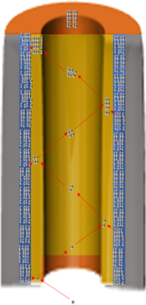
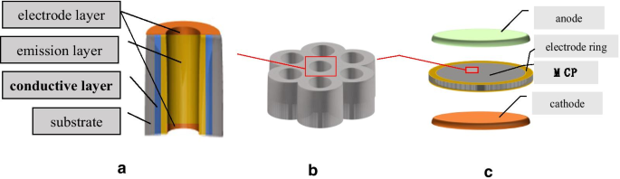
MCPの動作状態図
各マイクロチャネルは、検出器および電子増倍管として機能します。数百万のマイクロチャネルを独立して動作させることにより、MCPは、光子、電子、中性子、およびイオンを識別するために使用される、高い空間分解能、高いタイミング分解能、および広範囲のゲインの特性を備えています。 MCPは、光電検出器、光電子増倍管(PMT)、紫外線分光計、ブラウン管、走査型電子顕微鏡、電界放出ディスプレイ、残留ガス分析装置、医療画像、飛行時間型質量分析、夜間など、さまざまな種類の機器に統合できます。 -ビジョンゴーグルなど[1、4、7、8、9]。従来のプロセスの水素焼成により、マイクロチャネルは適切な導電率と二次電子放出係数になります。
マイクロチャネルの準備における水素焼成の通常のプロセスには多くの欠点があります。まず、水素焼成プロセスでは導電層と発光層を個別に調整できません[10、11]。第二に、重金属元素(Pb、Bi)は、鉛ガラスの製錬プロセスで環境汚染を引き起こします。第三に、MCPの広い領域は高温のためにゆがみます[8]。第4に、使用されている鉛ガラスの水素還元反応には、K、Rb、およびその他の放射性元素が含まれているため、バックグラウンドノイズが発生します[8]。最後に、細孔内に残留する水素はバイアス電圧によってイオンになり、電子の反対方向に飛んで機器の陰極を破壊します[8、12]。
初期の科学者は、水素焼成プロセスに代わるマイクロチャネル壁の導電層と発光層を成長させるソリューションを提案しています[3]。多くの薄膜堆積法では、マイクロチャネル内で長さと直径の比率が高い均一な膜を成長させることができません。アルゴンヌ国立研究所は、原子層堆積(ALD)を使用して、MCP上の導電層と発光層を成長させ、マイクロチャネル壁に無傷で均一な膜を実現することを提案しました[4、13]。さらに、ALD-MCPは前述の欠点を解決します。多くの研究機関は、MCPのパフォーマンスを向上させることができる競争力のある資料を見つけることを目指しています。
アルゴンヌ国立研究所は、MCP抵抗要件を考慮して、ALD-MCP導電層にAZO材料を選択します。抵抗が高すぎると、導電層が時間内に放出層に電子を補充できなくなり、MCPのゲインが低くなるか、動作しなくなります。一方、抵抗が低すぎると、MCPが過熱し、最終的に故障につながります[4、9、14、15]。したがって、導電層の設計はALD-MCPにとって重要です。
図2に示すように、AZO導電層の抵抗率がMCP抵抗要件の範囲内にある場合、許容されるZn含有量は非常に狭い範囲(70〜73%)になります[16]。したがって、MCPゲインは不安定であり、MCPは簡単に故障する可能性があります。 Znの代わりにWやMoなどの代替導電性材料が研究されています[3、4、17、18、19]。 \({\ text {WF}} _ {6} \)(\({\ text {MoF}} _ {6} \))と\({\ text {H}} _ {2}の化学反応{\ text {O}} \)は、ALDによってW(Mo)を成長させるために使用されます。ただし、\({\ text {WF}} _ {6} \)または\({\ text {MoF}} _ {6} \)を使用すると、2つの重大な欠点があります。腐食性が強く、不純物が含まれている可能性があります。製造工程で取り除くのは難しい。これらの理由から、これらの材料を使用したALD-MCPはコストがかかります。
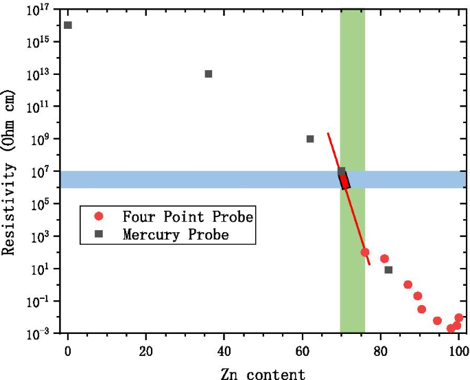
Zn含有量、Zn /(Zn + A)* 100(%)、MCP抵抗領域としての青色領域、AZO変化領域としての緑色領域、制御が必要な領域としての赤色領域
私たちの研究では、ZnOと\({\ text {Al}} _ {2} {\ text {O}} _ {3} \)を使用した合理的な設計が、MCP導電層で問題なく実現できることがわかりました。 WまたはMoが使用されている場合に直面し、価格でより競争力があります。ここでは、AZO導電層を備えたALD-MCPをAZO-ALD-MCPと名付けています。
導電性材料ZnOと高抵抗材料\({\ text {Al}} _ {2} {\ text {O}} _ {3} \)の比率を調整して、目的のAZO導電層特性を得るアルゴリズムを提案します。
MCPの動作抵抗(すなわち、マイクロチャネル内の電子なだれ中の抵抗)の概念を提唱しました。 AZO-ALD-MCPの動作抵抗をテストしたところ、AZO-ALD-MCPと従来のMCPの間に2つの違いが見つかりました。 AZO-ALD-MCPと従来のMCPの両方の動作抵抗と非動作抵抗が大幅に異なることがわかりました。さらに、AZO-ALD-MLPの抵抗は電圧と負の相関関係にあります。導電性材料と高抵抗材料の比率を調整するための私たちの提案(動作抵抗への参照)は、ALD-MCP導電層に使用される新しい材料を探して性能を向上させるのに役立つガイダンスを提供します将来のMCP。
実験と方法
成長するZnOと\({\ text {Al}} _ {2} {\ text {O}} _ {3} \)原子膜
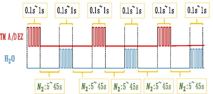
原子層堆積(ALD)は、前駆体と反応性ガスを基板の表面に交互に配置して、制御された速度で物理的または化学的吸着または表面飽和反応を実現する技術です。材料は、単原子膜表面の形で基板上に堆積されます。 ALDは、ピンホールのない、優れた被覆率の連続膜を生成でき、原子膜の厚さと組成を制御できます[1、2、4、11、13、19、20]。
以下は、ALDを使用してAl 2 を成長させる化学反応方程式です。 O 3 :
$$ \ begin {aligned}&{\ text {A}}:{\ text {Substrate}}-{\ text {OH}} ^ {*} + {\ text {Al}} \ left({{\ text {CH}} _ {3}} \ right)_ {3} \\&\ quad \ to {\ text {Substrate}}-{\ text {O}}-{\ text {Al}} \ left({ {\ text {CH}} _ {3}} \ right)_ {2} ^ {*} + {\ text {CH}} _ {4} \ uparrow \\&{\ text {B}}:{\ text {Substrate}}-{\ text {O}}-{\ text {Al}} \ left({{\ text {CH}} _ {3}} \ right)_ {2} ^ {*} + 2 {\ text {H}} _ {2} {\ text {O}} \\&\ quad \ to {\ text {Substrate}}-{\ text {O}}-{\ text {Al}} \ left ({{\ text {OH}}} \ right)_ {2} ^ {*} + 2 {\ text {CH}} _ {4} \ uparrow \\&{\ text {C}}:{\ text {Al}}-{\ text {OH}} ^ {*} + {\ text {Al}} \ left({{\ text {CH}} _ {3}} \ right)_ {3} \\ { }&\ quad \ to {\ text {Al}}-{\ text {O}}-{\ text {Al}} \ left({{\ text {CH}} _ {3}} \ right)_ { 2} ^ {*} + {\ text {CH}} _ {4} \ uparrow \\&{\ text {D}}:{\ text {Al}}-{\ text {CH}} _ {3} ^ {*} + {\ text {H}} _ {2} {\ text {O}} \ to {\ text {Al}}-{\ text {OH}} ^ {*} + 2 {\ text { CH}} _ {4} \ uparrow \\ \ end {aligned} $$反応の温度は60〜150°Cです。図3に示すように、Al 2 の層を成長させる時間と順序 O 3 アトムは:
成長するAl 2 O 3 およびZnO図
\({\ text {TMA}} / {\ text {N}} _ {2} / {\ text {H}} _ {2} {\ text {O}} / {\ text {N}} _ { 2} =0.1 \ sim1 {\ text {s}} / 5 \ sim45 {\ text {s}} / 0.1 \ sim1 {\ text {s}} / 5 \ sim45 {\ text {s}} \)。
以下は、ALDを使用してZnOを成長させるための化学反応方程式です。
$$ \ begin {aligned}&{\ text {E}}:{\ text {Substrate}}-{\ text {OH}} ^ {*} + {\ text {Zn}} \ left({{\ text {CH}} _ {2} {\ text {CH}} _ {3}} \ right)_ {2} \\&\ quad \ to {\ text {Substrate}}-{\ text {O}}- {\ text {ZnCH}} _ {2} {\ text {CH}} _ {3} ^ {*} + {\ text {CH}} _ {3} {\ text {CH}} _ {3} \ uparrow \\&{\ text {F}}:{\ text {Substrate}}-{\ text {O}}-{\ text {ZnCH}} _ {2} {\ text {CH}} _ {3} ^ {*} + {\ text {H}} _ {2} {\ text {O}} \\&\ quad \ to {\ text {Substrate}}-{\ text {O}}-{\ text { ZnOH}} ^ {*} + {\ text {CH}} _ {3} {\ text {CH}} _ {3} \ uparrow \\&{\ text {G}}:{\ text {Zn}} -{\ text {OH}} ^ {*} + {\ text {Zn}} \ left({{\ text {CH}} _ {2} {\ text {CH}} _ {3}} \ right) _ {2} \\&\ quad \ to {\ text {Zn}}-{\ text {O}}-{\ text {ZnCH}} _ {2} {\ text {CH}} _ {3} ^ {*} + {\ text {CH}} _ {3} {\ text {CH}} _ {3} \ uparrow \\&{\ text {H}}:{\ text {Zn}}-{\ text {CH}} _ {2} {\ text {CH}} _ {3} ^ {*} + {\ text {H}} _ {2} {\ text {O}} \ to {\ text {Zn} }-{\ text {OH}} ^ {*} + {\ text {CH}} _ {3} {\ text {CH}} _ {3} \ uparrow \\ \ end {aligned} $$反応の温度は60〜150°Cです。図3に示すように、ZnO原子の層を成長させる時間と順序は次のとおりです。
$$ {\ text {DEZ}} / {\ text {N}} _ {2} / {\ text {H}} _ {2} {\ text {O}} / {\ text {N}} _ { 2} =0.1 \ sim1 {\ text {s}} / 5 \ sim45 {\ text {s}} / 0.1 \ sim1 {\ text {s}} / 5 \ sim45 {\ text {s}} {。} $ $AZO導電層の設計
AZOの厚さは通常300から1000原子層の範囲です。導電性材料であるZnOと高抵抗性材料であるAl2O3の比率を調整するために、Al2O3とZnOの原子層の次数を設計するための新しい数学演算ルールを定義します。
$$ \ left(\ begin {array} {* {20} c} {{\ text {mA}}} \\ {{\ text {mB}}} \\ \ vdots \\ \ end {array} \ right )={\ text {m}} \ left(\ begin {array} {* {20} c} {\ text {A}} \\ {\ text {B}} \\ \ vdots \\ \ end {array } \ right)$$(1)$$ \ begin {aligned}&{\ text {A}} \ left(\ begin {array} {* {20} c} {\ text {a}} \\ {\ text {b}} \\ \ vdots \\ \ end {array} \ right)+ {\ text {B}} \ left(\ begin {array} {* {20} c} {\ text {c}} \ \ {\ text {d}} \\ \ vdots \\ \ end {array} \ right)+ {\ text {C}} \ left(\ begin {array} {* {20} c} {\ text {e }} \\ {\ text {f}} \\ \ vdots \\ \ end {array} \ right)\ ldots \\&\ quad =\ left(\ begin {array} {* {20} c} {\ text {A}} \\ {\ text {B}} \\ \ vdots \\ \ end {array} \ right)\ left [\ left(\ begin {array} {* {20} c} {\ text { a}} \\ {\ text {b}} \\ \ vdots \\ \ end {array} \ right)\ left(\ begin {array} {* {20} c} {\ text {c}} \\ {\ text {d}} \\ \ vdots \\ \ end {array} \ right)\ left(\ begin {array} {* {20} c} {\ text {e}} \\ {\ text {f }} \\ \ vdots \\ \ end {array} \ right)\ ldots \ right] =\ left(\ begin {array} {* {20} c} {{\ text {Aa}} + {\ text { Bc}} + {\ text {Ce}} + \ ldots } \\ {{\ text {Ab}} + {\ text {Bd}} + {\ text {Cf}} + \ ldots} \\ \ vdots \\ \ end {array} \ right)\\ \ end {整列} $$(2)数学演算はWYM演算と名付けられました。 WYM操作には、2つのプロパティと数式があります。
WYMプロパティ1:
$$ \ begin {aligned}&\ left({\ begin {array} {* {20} c} {\ text {m}} \\ {\ text {n}} \\ \ end {array}} \ right )\ left [{\ left({\ begin {array} {* {20} c} {\ text {a}} \\ {\ text {b}} \\ \ end {array}} \ right)\ left ({\ begin {array} {* {20} c} {\ text {c}} \\ {\ text {d}} \\ \ end {array}} \ right)} \ right] \ left [{\ left({\ begin {array} {* {20} c} {\ text {e}} \\ {\ text {f}} \\ \ end {array}} \ right)\ left({\ begin {array } {* {20} c} {\ text {g}} \\ {\ text {h}} \\ \ end {array}} \ right)} \ right] \ left [{\ left({\ begin { array} {* {20} c} {\ text {i}} \\ {\ text {j}} \\ \ end {array}} \ right)\ left({\ begin {array} {* {20} c} {\ text {k}} \\ {\ text {l}} \\ \ end {array}} \ right)} \ right] \ ldots \\&\ quad =\ left({\ begin {array} {* {20} c} {\ text {m}} \\ {\ text {n}} \\ \ end {array}} \ right)\ left \ {{\ left({\ begin {array} {* {20} c} {\ text {a}} \\ {\ text {b}} \\ \ end {array}} \ right)\ left [{\ left({\ begin {array} {* {20} c} {\ text {e}} \\ {\ text {f}} \\ \ end {array}} \ right)\ left({\ begin {array} {* {20} c} {\ text {g }} \\ {\ text {h}} \\ \ end {array}} \ right)} \ right]、\ left({\ beg in {array} {* {20} c} {\ text {c}} \\ {\ text {d}} \\ \ end {array}} \ right)\ left [{\ left({\ begin {array } {* {20} c} {\ text {e}} \\ {\ text {f}} \\ \ end {array}} \ right)\ left({\ begin {array} {* {20} c } {\ text {g}} \\ {\ text {h}} \\ \ end {array}} \ right)} \ right]} \ right \} \ left [{\ left({\ begin {array} {* {20} c} {\ text {i}} \\ {\ text {j}} \\ \ end {array}} \ right)\ left({\ begin {array} {* {20} c} {\ text {k}} \\ {\ text {l}} \\ \ end {array}} \ right)} \ right] \ ldots \\&\ quad =\ left({\ begin {array} {* {20} c} {\ text {m}} \\ {\ text {n}} \\ \ end {array}} \ right)\ left [{\ left({\ begin {array} {* {20} c} {\ text {a}} \\ {\ text {b}} \\ \ end {array}} \ right)\ left({\ begin {array} {* {20} c} {\ text {c }} \\ {\ text {d}} \\ \ end {array}} \ right)} \ right] \ left \ {{\ left({\ begin {array} {* {20} c} {\ text {e}} \\ {\ text {f}} \\ \ end {array}} \ right)\ left [{\ left({\ begin {array} {* {20} c} {\ text {i} } \\ {\ text {j}} \\ \ end {array}} \ right)\ left({\ begin {array} {* {20} c} {\ text {k}} \\ {\ text { l}} \\ \ end {array}} \ right)} \ right]、\ left({\ begin {array} {* {20} c} {\ te xt {g}} \\ {\ text {h}} \\ \ end {array}} \ right)\ left [{\ left({\ begin {array} {* {20} c} {\ text {i }} \\ {\ text {j}} \\ \ end {array}} \ right)\ left({\ begin {array} {* {20} c} {\ text {k}} \\ {\ text {l}} \\ \ end {array}} \ right)} \ right]} \ right \} \ ldots \\ \ end {aligned} $$WYMプロパティ2:
$$ \ begin {aligned}&{\ text {A}} \ left({\ begin {array} {* {20} c} {\ text {m}} \\ {\ text {n}} \\ \ end {array}} \ right)\ left [{\ left({\ begin {array} {* {20} c} {\ text {a}} \\ {\ text {b}} \\ \ end {array }} \ right)\ left({\ begin {array} {* {20} c} {\ text {c}} \\ {\ text {d}} \\ \ end {array}} \ right)} \ right] \ left [{\ left({\ begin {array} {* {20} c} {\ text {e}} \\ {\ text {f}} \\ \ end {array}} \ right)\ left({\ begin {array} {* {20} c} {\ text {g}} \\ {\ text {h}} \\ \ end {array}} \ right)} \ right] \ ldots \\ &\ quad =\ left({\ begin {array} {* {20} c} {{\ text {Am}}} \\ {{\ text {An}}} \\ \ end {array}} \ right )\ left [{\ left({\ begin {array} {* {20} c} {\ text {a}} \\ {\ text {b}} \\ \ end {array}} \ right)\ left ({\ begin {array} {* {20} c} {\ text {c}} \\ {\ text {d}} \\ \ end {array}} \ right)} \ right] \ left [{\ left({\ begin {array} {* {20} c} {\ text {e}} \\ {\ text {f}} \\ \ end {array}} \ right)\ left({\ begin {array } {* {20} c} {\ text {g}} \\ {\ text {h}} \\ \ end {array}} \ right)} \ right] \ ldots \\&\ quad =\ left( {\ begin {array} {* {20} c} {\ text {m}} \\ {\ text {n}} \\ \ end {a rray}} \ right)\ left [{{\ text {A}} \ left({\ begin {array} {* {20} c} {\ text {a}} \\ {\ text {b}} \ \ \ end {array}} \ right)、{\ text {A}} \ left({\ begin {array} {* {20} c} {\ text {c}} \\ {\ text {d}} \\ \ end {array}} \ right)} \ right] \ left [{\ left({\ begin {array} {* {20} c} {\ text {e}} \\ {\ text {f} } \\ \ end {array}} \ right)\ left({\ begin {array} {* {20} c} {\ text {g}} \\ {\ text {h}} \\ \ end {array }} \ right)} \ right] \ ldots \\&\ quad =\ left({\ begin {array} {* {20} c} {\ text {m}} \\ {\ text {n}} \ \ \ end {array}} \ right)\ left [{\ left({\ begin {array} {* {20} c} {\ text {a}} \\ {\ text {b}} \\ \ end {array}} \ right)\ left({\ begin {array} {* {20} c} {\ text {c}} \\ {\ text {d}} \\ \ end {array}} \ right) } \ right] \ left [{{\ text {A}} \ left({\ begin {array} {* {20} c} {\ text {e}} \\ {\ text {f}} \\ \ end {array}} \ right)、{\ text {A}} \ left({\ begin {array} {* {20} c} {\ text {g}} \\ {\ text {h}} \\ \ end {array}} \ right)} \ right] \ ldots \\ \ end {aligned} $$WYM式:
$$ \ begin {aligned}&\ left(\ begin {array} {* {20} c} {\ text {a}} \\ {\ text {b}} \\ \ vdots \\ \ end {array} \ right)=\ left(\ begin {array} {* {20} c} {{\ text {A}} + \ frac {{\ text {X}}} {{\ text {Y}}}} \ \ {\ text {b}} \\ \ vdots \\ \ end {array} \ right)\ propto {\ text {Y}} \ left(\ begin {array} {* {20} c} {{\ text {A}} + \ frac {{\ text {X}}} {{\ text {Y}}}} \\ {\ text {b}} \\ \ vdots \\ \ end {array} \ right)=\ left({\ begin {array} {* {20} c} {{\ text {Y}}-{\ text {X}}} \\ {\ text {X}} \\ \ end {array}} \ right)\ left [\ left(\ begin {array} {* {20} c} {\ text {A}} \\ {\ text {b}} \\ \ vdots \\ \ end {array} \ right )\ left(\ begin {array} {* {20} c} {{\ text {A}} + 1} \\ {\ text {b}} \\ \ vdots \\ \ end {array} \ right) \ right] \\&\ left(\ begin {array} {* {20} c} {\ text {a}} \\ {\ text {b}} \\ \ vdots \\ \ end {array} \ right )=\ left(\ begin {array} {* {20} c} {\ text {a}} \\ {{\ text {B}} + \ frac {{\ text {X}}} {{\ text {Y}}}} \\ \ vdots \\ \ end {array} \ right)\ propto {\ text {Y}} \ left(\ begin {array} {* {20} c} {\ text {a} } \\ {{\ text {B}} + \ frac {{\ text {X}}} {{\ text {Y}}}} \\ \ vdots \\ \ end {array} \ right)=\ left({\ begin {array} {* {20} c} {{\ text {Y}}-{\ text {X}}} \\ {\ text {X}} \\ \ end {array}} \ right)\ left [\ left(\ begin {array} {* {20} c} {\ text {a}} \\ {\ text {B}} \\ \ vdots \\ \ end {array} \ right )\ left(\ begin {array} {* {20} c} {\ text {a}} \\ {{\ text {B}} + 1} \\ \ vdots \\ \ end {array} \ right) \ right] \\ \ end {aligned} $$小文字は実数を表し、大文字は整数を表すことに注意してください。例1と例2では、操作の実行を示しています。
例1
$$ \ left({\ begin {array} {* {20} c} {{\ text {ZnO}}} \\ {{\ text {Al}} _ {2} {\ text {O}} _ { 3}} \\ \ end {array}} \ right)=\ left({\ begin {array} {* {20} c} {4 + \ frac {1} {2}} \\ 1 \\ \ end {array}} \ right)\ propto \ left({\ begin {array} {* {20} c} 1 \\ 1 \\ \ end {array}} \ right)\ left [{\ left({\ begin {array} {* {20} c} 4 \\ 1 \\ \ end {array}} \ right)\ left({\ begin {array} {* {20} c} 5 \\ 1 \\ \ end { array}} \ right)} \ right] =\ left({\ begin {array} {* {20} c} 4 \\ 1 \\ \ end {array}} \ right)+ \ left({\ begin { array} {* {20} c} 5 \\ 1 \\ \ end {array}} \ right)$$この操作は、\(\ left({\ begin {array} {* {20} c} 4 \\ 1 \\ \ end {array}} \ right)\)と\(\ left( {\ begin {array} {* {20} c} 5 \\ 1 \\ \ end {array}} \ right)\)。最初のスキームでは、4倍のZnO原子層と1つのAl2O3原子層を成長させます。 2番目のスキームでは、5倍のZnO原子層と1つのAl2O3原子層を成長させます。これら2つのスキームを2回繰り返すと、図4のような構造になります。
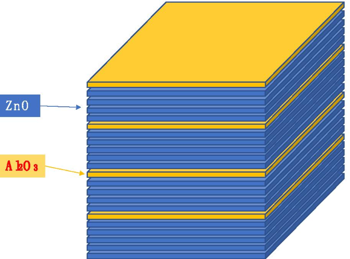
ZnOとAl 2 の概略図 O 3 成長シーケンス
操作ルールのより複雑な使用法を例2に示します。
$$ \ begin {aligned}&\ left({\ begin {array} {* {20} c} {{\ text {ZnO}}} \\ {{\ text {Al}} _ {2} {\ text {O}} _ {3}} \\ \ end {array}} \ right)=\ left({\ begin {array} {* {20} c} {4.71} \\ 1 \\ \ end {array} } \ right)=\ left({\ begin {array} {* {20} c} {4 + 0.71} \\ 1 \\ \ end {array}} \ right)\\&\ frac {2} {3 } =0.666 <0.71 <\ frac {3} {4} =0.75 \\&\ left({\ begin {array} {* {20} c} E \\ F \\ \ end {array}} \ right) \ left [{\ left({\ begin {array} {* {20} c} {4 + \ frac {2} {3}} \\ 1 \\ \ end {array}} \ right)\ left({ \ begin {array} {* {20} c} {4 + \ frac {3} {4}} \\ 1 \\ \ end {array}} \ right)} \ right] \\&\ quad =E \ left({\ begin {array} {* {20} c} {4 + \ frac {2} {3}} \\ 1 \\ \ end {array}} \ right)+ F \ left({\ begin { array} {* {20} c} {4 + \ frac {3} {4}} \\ 1 \\ \ end {array}} \ right)=\ left({\ begin {array} {* {20} c} {4E + 4F + \ frac {2} {3} E + \ frac {3} {4} F} \\ {E + F} \\ \ end {array}} \ right)\\&\ quad =E + F \ left({\ begin {array} {* {20} c} {4 + \ frac {{\ frac {2} {3} E + \ frac {3} {4} F}} {E + F}} \\ 1 \\ \ end {array}} \ right)\ propto \ left({\ begin {array} {* {20} c} {4 + \ frac {{\ frac {2} {3} E + \ frac {3} {4} F}} {E + F}} \\ 1 \\ \ end {array}} \ right)=\ left({\ begin {array} {* {20} c} {4.71} \\ 1 \\ \ end {array}} \ right)\\&\ frac {{\ frac {2} { 3} E + \ frac {3} {4} F}} {E + F} =0.71 \ Rightarrow {\ text {E}} =12、{\ text {F}} =13 \\&\ left({ \ begin {array} {* {20} c} E \\ F \\ \ end {array}} \ right)=\ left({\ begin {array} {* {20} c} {12} \\ { 13} \\ \ end {array}} \ right)=12 \ left({\ begin {array} {* {20} c} 1 \\ {1 \ frac {1} {12}} \\ \ end { array}} \ right)=\ left({\ begin {array} {* {20} c} {11} \\ 1 \\ \ end {array}} \ right)\ left [{\ left({\ begin {array} {* {20} c} 1 \\ 1 \\ \ end {array}} \ right)\ left({\ begin {array} {* {20} c} 1 \\ 2 \\ \ end { array}} \ right)} \ right] \\&\ left({\ begin {array} {* {20} c} E \\ F \\ \ end {array}} \ right)\ left [{\ left ({\ begin {array} {* {20} c} {4 + \ frac {2} {3}} \\ 1 \\ \ end {array}} \ right)、\ left({\ begin {array} {* {20} c} {4 + \ frac {3} {4}} \\ 1 \\ \ end {array}} \ right)} \ right] \\&\ quad =\ left({\ begin { array} {* {20} c} E \\ F \\ \ end {array}} \ right)\ left [{ \ left({\ begin {array} {* {20} c} 1 \\ 2 \\ \ end {array}} \ right)\ left [{\ left({\ begin {array} {* {20} c } 4 \\ 1 \\ \ end {array}} \ right)\ left({\ begin {array} {* {20} c} 5 \\ 1 \\ \ end {array}} \ right)} \ right ]、\ left({\ begin {array} {* {20} c} 1 \\ 3 \\ \ end {array}} \ right)\ left [{\ left({\ begin {array} {* {20 } c} 4 \\ 1 \\ \ end {array}} \ right)\ left({\ begin {array} {* {20} c} 5 \\ 1 \\ \ end {array}} \ right)} \ right]} \ right] \\&\ left({\ begin {array} {* {20} c} {4.71} \\ 1 \\ \ end {array}} \ right)\ propto \ left({\ begin {array} {* {20} c} {12} \\ {13} \\ \ end {array}} \ right)\ left [{\ left({\ begin {array} {* {20} c} 1 \\ 2 \\ \ end {array}} \ right)\ left({\ begin {array} {* {20} c} 1 \\ 3 \\ \ end {array}} \ right)} \ right] \ left [{\ left({\ begin {array} {* {20} c} 4 \\ 1 \\ \ end {array}} \ right)\ left({\ begin {array} {* {20} c } 5 \\ 1 \\ \ end {array}} \ right)} \ right] =\ left({\ begin {array} {* {20} c} {11} \\ 1 \\ \ end {array} } \ right)\ left [{\ left({\ begin {array} {* {20} c} 1 \\ 1 \\ \ end {array}} \ right)\ left({\ begin {array} {* {20} c } 1 \\ 2 \\ \ end {array}} \ right)} \ right] \ left [{\ left({\ begin {array} {* {20} c} 1 \\ 2 \\ \ end {array }} \ right)\ left({\ begin {array} {* {20} c} 1 \\ 3 \\ \ end {array}} \ right)} \ right] \ left [{\ left({\ begin {array} {* {20} c} 4 \\ 1 \\ \ end {array}} \ right)\ left({\ begin {array} {* {20} c} 5 \\ 1 \\ \ end {配列}} \ right)} \ right] \\ \ end {aligned} $$プラン1 :\(\ left({\ begin {array} {* {20} c} {4.71} \\ 1 \\ \ end {array}} \ right)\ propto 12 \ left [{\ left({\ begin { array} {* {20} c} 4 \\ 1 \\ \ end {array}} \ right)+ 2 \ left({\ begin {array} {* {20} c} 5 \\ 1 \\ \ end {array}} \ right)} \ right] + 13 \ left [{\ left({\ begin {array} {* {20} c} 4 \\ 1 \\ \ end {array}} \ right)+ 3 \ left({\ begin {array} {* {20} c} 5 \\ 1 \\ \ end {array}} \ right)} \ right] \)。
プラン2 \(\ left({\ begin {array} {* {20} c} {4.71} \\ 1 \\ \ end {array}} \ right)\ propto 11 \ left [{\ left [{\ left({ \ begin {array} {* {20} c} 4 \\ 1 \\ \ end {array}} \ right)+ 2 \ left({\ begin {array} {* {20} c} 5 \\ 1 \ \ \ end {array}} \ right)} \ right] + \ left [{\ left({\ begin {array} {* {20} c} 4 \\ 1 \\ \ end {array}} \ right) + 3 \ left({\ begin {array} {* {20} c} 5 \\ 1 \\ \ end {array}} \ right)} \ right]} \ right] + \ left [{\ left [{ \ left({\ begin {array} {* {20} c} 4 \\ 1 \\ \ end {array}} \ right)+ 2 \ left({\ begin {array} {* {20} c} 5 \\ 1 \\ \ end {array}} \ right)} \ right] + 2 \ left [{\ left({\ begin {array} {* {20} c} 4 \\ 1 \\ \ end {array }} \ right)+ 3 \ left({\ begin {array} {* {20} c} 5 \\ 1 \\ \ end {array}} \ right)} \ right]} \ right] \)。
例2では、プラン1の操作は次のように解釈できます。
スキーム1 ALDは、ZnO原子層成長プロセスを4回、\({\ text {Al}} _ {2} {\ text {O}} _ {3} \)原子層成長プロセスを1回成長させます。 ALDは、ZnO原子層成長プロセスを5回、\({\ text {Al}} _ {2} {\ text {O}} _ {3} \)原子層成長プロセスを1回成長させ、2回繰り返します。
スキーム2 ALDは、ZnO原子層成長プロセスを4回、\({\ text {Al}} _ {2} {\ text {O}} _ {3} \)原子層成長プロセスを1回成長させます。 ALDは、ZnO原子層成長プロセスを5回、\({\ text {Al}} _ {2} {\ text {O}} _ {3} \)原子層成長プロセスを1回成長させ、3回繰り返します。
>スキーム1を12回繰り返し、スキーム2を13回繰り返します。
プラン2の操作の解釈は、プラン1と同じ線に沿っています。
マイクロチャネルプレート抵抗テスト
図5aに示すように、原子層堆積技術を使用して、AZO導電層と\({\ text {Al}} _ {2} {\ text {O}} _ {3} \)発光層を成長させます。二次元細孔アレイのマイクロチャネル壁。次に、熱蒸着技術を使用して、MCPの両側にNi–Cr電極層を成長させ[2、4]、MCPの両側に電極リングを配置します。上記の準備をして、ALD-MCP耐性を直接テストします。この状態では、対応するMCP抵抗をMCPの非動作抵抗として定義します。ケースレーモデル6517B電位計を使用して、MCPの非動作抵抗を10 -3 で測定します。 –10 -5 Pa真空[1、4、13]。
ALD-MCP抵抗テストの概略図
図5cに示すように、カソードとして電子銃を使用し、アノードとしてリン光スクリーンを使用します。電子銃はMCPに入射電子を提供し、リン光スクリーンはMCPによって出力された電子を受け取ります。さらに、MCPの動作中は、高電圧リン光スクリーンが緑色の光を発して、MCPの均一性を検出します[1,21]。
図1に示すように、電流を測定するためのMCPの入力として100pAを提供する電子銃を使用します。二次電子の数が増えると、放出層が大量の電荷を失い、導電層が放出層に電荷の流れを継続的に提供する状態が発生します。この状態で、対応するMCP抵抗をMCPの動作抵抗として定義します。動作抵抗の真空環境は10 -3 –10 -5 Pa。
結果と考察
AZO-ALD-MCPサンプルの断面SEM写真を図6に示します。表1に示すように一連のAZO導電層を設計し、それに対応する動作抵抗と非動作抵抗を図7に示します。同じ図で、従来のMCPの動作抵抗と非動作抵抗も示しています。 AZO-ALD-MCPの非作動抵抗と比較して、AZO-ALD-MCPの作動抵抗は大幅に減少します。ただし、従来のMCPの作動抵抗と非作動抵抗の間に有意差はありません。電圧が上昇すると、AZO-ALD-MCPの動作抵抗は従来のMCPの動作抵抗よりも大幅に低くなります。同じ電圧条件下で、AZO-ALD-MCPの動作抵抗と非動作抵抗は安定しています。前述の特徴には主に2つの理由があると考えています。
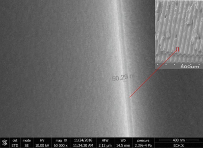
AZO-ALD-MCPの断面SEM写真
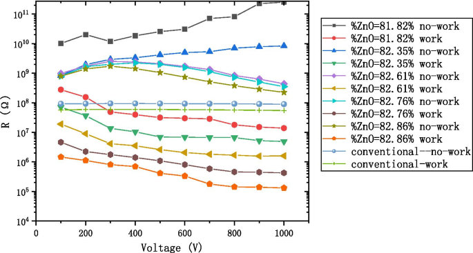
異なる比率のAZO-ALD-MCPと従来のMCPでの電圧図による動作抵抗と非動作抵抗
式[21]によると、
$$ R _ {{{\ text {MCP}}}} =R_ {0} \ exp \ left [{-\ beta_ {T} \ left({T _ {{{\ text {MCP}}}}-T_ { 0}} \ right)} \ right] $$鉛ガラスと比較して、AZOは負の温度係数(NTC)が高い材料であるため、同じ温度と初期抵抗で抵抗が低くなります。ゲインを生成する過程で、AZOは高電圧で入射電子の衝撃を受け、それによってより多くの電子正孔対が生成され、電流が増加します。
<図>材料抵抗の安定性を説明するために、非動作抵抗と動作抵抗の比率を定義します。
$$ \ kappa_ {R} =\ frac {{R_ {n}}} {{R_ {w}}} $$図8は、AZO-ALD-MCPの\(\ kappa_ {R} \)が約10 2 であることを示しています。 –10 3 倍であり、従来のMCPの\(\ kappa_ {R} \)は約2〜3倍です。これは、AZO-ALD-MCPの抵抗変化がより明白であることを示しています。したがって、MCP抵抗の定義としての非動作抵抗の古い概念は、代わりに動作抵抗に置き換える必要があります。
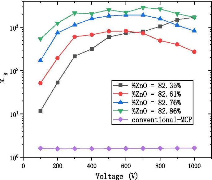
K R AZO-ALD-MCPの異なる比率での電圧図を使用
図9は、動作電圧に対する「隣接する」マテリアルデザインからの抵抗の比率\(L_ {R} \)を示しています。比率\(L_ {R} \)は次のように定義されます:
$$ L_ {R} =\ frac {{R \ left({4 + \ frac {N-1} {N}} \ right)}} {{R \ left({4 + \ frac {N} {N + 1}} \ right)}} $$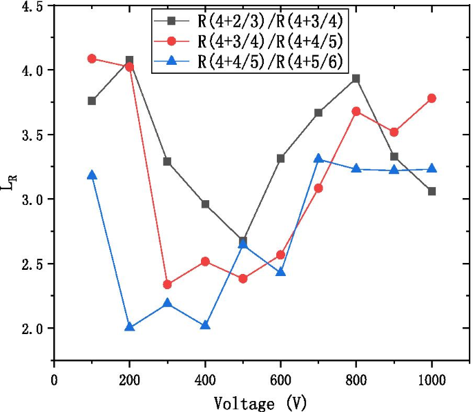
The resistance of the step length LR with the voltage diagram at the different ratio of the working resistance of neighbor formula
ここで
$$\left( {\begin{array}{*{20}c} {{\text{ZnO}}} \\ {{\text{Al}}_{2} {\text{O}}_{3} } \\ \end{array} } \right) =\left( {\begin{array}{*{20}c} {4 + \frac{N - 1}{N}} \\ 1 \\ \end{array} } \right) =\left( {\begin{array}{*{20}c} 1 \\ {N - 1} \\ \end{array} } \right)\left[ {\left( {\begin{array}{*{20}c} 4 \\ 1 \\ \end{array} } \right)\left( {\begin{array}{*{20}c} 5 \\ 1 \\ \end{array} } \right)} \right]$$および
$$\left( {\begin{array}{*{20}c} {{\text{ZnO}}} \\ {{\text{Al}}_{2} {\text{O}}_{3} } \\ \end{array} } \right) =\left( {\begin{array}{*{20}c} {4 + \frac{N}{N + 1}} \\ 1 \\ \end{array} } \right) =\left( {\begin{array}{*{20}c} 1 \\ N \\ \end{array} } \right)\left[ {\left( {\begin{array}{*{20}c} 4 \\ 1 \\ \end{array} } \right)\left( {\begin{array}{*{20}c} 5 \\ 1 \\ \end{array} } \right)} \right]$$As can be observed from Fig. 9, the LR value ranges from 2 to 4.5 to adjust ratio of conductive material ZnO and high resistance material \({\text{Al}}_{2} {\text{O}}_{3}\). And it proves the feasibility of WYM operation to design laminated materials.
Figure 10 shows the working resistance with respect to the percentage of ZnO cycles (%ZnO), where %ZnO is defined to be:
$${\text{\% ZnO}} =\frac{{{\text{ZnO}}}}{{{\text{ZnO}} + {\text{Al}}_{2} {\text{O}}_{3} }}{*}100\left( {\text{\% }} \right)$$
The working resistance with the percentage of ZnO cycles diagram at the different voltage
under various voltage conditions, ranging from 100 to 1000 V. It decreases that the working resistance under the same voltage with the increase in the percentage of ZnO cycles. It can be the same that the working resistance under different the percentage of ZnO cycles and under the different condition of voltage. Therefore, the AZO-ALD-MCP of different formulations works under its specific voltage to meet the MCP resistance index.
We define the ratio of the resistance difference under the different condition of voltage and the voltage difference to describe the effect of the voltage on the resistance of MCP:
$$r =\left| {\frac{{R_{U} - R_{V} }}{U - V}} \right| =\ left | {\frac{{R_{1000v} - R_{100v} }}{1000 - 100}} \right|$$Figure 11 shows that the effect of the voltage on the resistance of AZO-ALD-MCP decreased and gradually stabilized with the increase in the percentage of ZnO cycles. Therefore, the preparation of AZO-ALD-MCP should try to choose a formula with a large percentage of ZnO cycles.

The r with the percentage of ZnO cycles diagram at the working state
Based on the above analysis, we have put forward the reference to the working resistance for the conductive layer of ALD-MCP. As shown in Fig. 5a, we design the AZO conductive layer of AZO-MCP by using the WYM operation and temperature adjustment based on the working resistance. We use atomic layer deposition technology to grow the \({\text{Al}}_{2} {\text{O}}_{3}\) emission layer on microchannel wall of the two-dimensional pore arrays [3, 11, 22]. In Fig. 12a, the gain from our AZO-ALD-MCP is compared to that of a conventional MCP under different voltages. As can be observed, our preparation method of the AZO-ALD-MCP provides a larger gain than that of a conventional MCP. Figure 12b shows the phosphor screen with uniform green light under high pressure, thus proving the uniformity of the material deposited on the wall of each microchannel and the uniformity of the AZO-ALD-MCP field of view.

The gain with the voltage diagram at the AZO-ALD-MCP and conventional-MCP
結論
We defined the working and non-working resistance of the microchannel plate. Aiming at the required resistivity of the microchannel plate in the region with extremely narrow zinc content requirement (70–73%), an algorithm for growing the AZO conductive layer is proposed. Compared with the conventional MCP, we found a large difference between the working and non-working resistance and there is also a huge difference under different voltages. Therefore, we analyze the data by defining \(\kappa_{R} ,L_{R} ,\% {\text{ZnO}},r\). MCP should try to choose a formula with a large percentage of ZnO cycles. We recommend using the working resistance as an ALD-MCP resistance indicator in industrial production. Building on our results as described in this work, our studies will help to find even better materials as the conductive layer for the ALD-MCP.
変更履歴
ナノマテリアル